Abstract
Opto-spintronics is an emerging field that focuses on harnessing light to manipulate and analyze electron spins to develop next-generation electronic devices. This paper explores recent progress and the role of solid-state materials in opto-spintronics by focusing on key classes of materials, such as ferromagnetic semiconductors, two-dimensional (2D) transition metal dichalcogenides (TMDCs), and topological insulators. It examines the unique properties of ferromagnetic and antiferromagnetic materials and their ability to interact with light to affect spin dynamics, offering potential for improved sensing and quantum computing. By combining opto-spintronics with solid-state systems, spintronic devices could become faster and more efficient, leading to new technological advancements and scalable technologies.
1. Introduction
Opto-spintronics represents a burgeoning area of research that merges the principles of optics and spintronics to explore and manipulate the spin properties of electrons in solid materials [1]. This field leverages the interaction between light and electron spins to achieve control over magnetic states, which is crucial for the development of next-generation electronic devices. Traditional spintronics has primarily focused on ferromagnetic materials, where the alignment of spins allows for the storage and retrieval of magnetic information. However, recent advancements have highlighted the potential of antiferromagnetic materials, which, despite being less utilized, offer unique benefits such as faster dynamics and robustness against external magnetic fields. The study of opto-spintronics in solid-state systems is particularly promising due to the diverse range of materials available, including two-dimensional (2D) [2,3,4,5] and three-dimensional (3D) [6] semiconductor heterostructures. These materials provide a versatile platform for investigating charge dynamics and spin interactions, as demonstrated in recent research involving WSe2/GaAs heterostructures [7]. By integrating optical techniques with spintronic devices, researchers aim to enhance the performance and functionality of electronic systems, potentially leading to breakthroughs in quantum information processing and high-speed data transmission [8,9]. This review delves into the current state of research in opto-spintronics, focusing on the role of solid materials and their applications. It aims to provide a comprehensive overview of the field, highlighting key developments and future directions for research and technology. This review is structured as follows: Section 2 presents the fundamental mechanisms of opto-spintronics, including light–spin interactions, spin–orbit torque, and optical spin transfer; Section 3 highlights recent advancements and application areas such as quantum information processing, energy harvesting, and room-temperature spin control. Special attention is provided to emerging materials, including two-dimensional magnets and molecular spin systems; Section 4 concludes with a summary of key insights and future research directions in the field of solid-state opto-spintronics.
2. Fundamentals
2.1. Light–Spin Interactions
Opto-spintronics controls magnetic order on ultrashort time scales by employing light to interact with spin systems in materials. In contrast to conventional methods, this interaction allows a non-invasive way to investigate and control magnetic characteristics much more quickly. Based on the wavelength of light employed, the field is separated into three categories: visible, Ultraviolet (UV) to X-rays, and GHz to THz [10,11]. Each category has its own set of challenges and uses. Many significant developments in modern physics and business, ranging from quantum information science to spin-based electronics, or spintronics, are based on light–spin interactions. This subject examines the dynamic interaction between spin degrees of freedom and electromagnetic radiation, which has long piqued the curiosity of theorists and experimentalists both. Understanding the relationship between the intrinsic angular momentum of light, or spin, and the spin of particles such as electrons, nuclei, or atomic ensembles is the fundamental objective of research on light–spin interactions.
Historical milestones in this discipline include the creation of methods that depend on these fundamental interactions, such as nuclear magnetic resonance (NMR) and electron paramagnetic resonance (EPR). The field of light–spin interaction research has grown rapidly with the introduction of laser technology, ultrafast optics, and high-precision magnetic field control. These days, new quantum technologies like secure quantum communications and quantum computing are being developed using the principles of light–spin coupling [12]. Designing devices where spin control and quantum coherence are essential and require an understanding of these processes. Thanks to developments in nanotechnology and materials science, scientists are now investigating intricate spin dynamics in artificial systems like topological insulators and quantum dots.
An understanding of spin and angular momentum is fundamental to the study of light–spin interactions. In quantum mechanics, the spin, known as an intrinsic type of angular momentum, is mathematically described by the Pauli matrices. Although spin is different from the orbital angular momentum involved in a particle’s passage through space, it is subject to the same basic commutation relations and conservation rules. Spin angular momentum (SAM) and orbital angular momentum (OAM) are the two primary kinds of angular momentum carried by light, an electromagnetic wave [13]. SAM is linked to light polarization, such as elliptical or circular polarization, in which the electric field vector revolves around the propagation direction.
The Lorentz force law and Maxwell’s equations are used in classical electrodynamics to explain how light interacts with a magnetic dipole, such as an electron spin [14]. Quantum electrodynamics (QED), in which the interaction is mediated by virtual photons and controlled by the laws of quantum field theory, is necessary for a more accurate description. For both basic physics and real-world uses, such as creating spin-based transistors and novel quantum sensors, it is essential to comprehend how light affects spin dynamics and vice versa.
2.2. Optical Spin Transfer and Spin–Orbit Torque
In the ongoing search for more powerful and efficient electronic devices, the field of spintronics has shown great promise. Spin–orbit torque and optical spin transfer are two intriguing phenomena at the core of this research. These processes provide new ways to control the magnetization of materials, opening the door for next-generation communication, processing, and data-storage systems. Using state-of-the-art research and professional perspectives, this in-depth account explores the fundamentals, workings, applications, difficulties, and potential futures of optical spin transfer and spin–orbit torque.
2.3. Fundamentals of Spintronics
2.3.1. Spintronics
The primary goal of spintronics, also known as spin electronics, is to actively control and manipulate spin degrees of freedom in solid-state systems. Spintronics develops new types of electrical devices by employing both the charge and intrinsic spin of electrons, as opposed to conventional electronics, which mostly exploits the charge. This technology has already produced major scientific and commercial breakthroughs, such as the discovery of magnetoresistance, which revolutionized hard disk drive read heads and allowed for the development of magnetic random-access memory (MRAM) [15,16]. The study of unique physical processes and prospective applications is advancing the area of spintronics.
2.3.2. Spin–Orbit Interactions
A fundamental mechanism in spintronics is the spin–orbit interaction, which results from the coupling of an electron’s orbital motion and spin [17]. In materials, this interaction is essential for producing spin currents and torques, especially in systems with a strong spin–orbit coupling. One particular kind of torque that arises from the spin–orbit interaction in a nearby normal metal is called spin–orbit torque (SOT) [18,19,20]. It is produced when a spin–orbit coupled material’s in-plane electric current produces a perpendicular spin current that can apply torque to a nearby magnetic layer. Among the many ways that SOT outperforms spin-transfer torque (STT) is the capacity to isolate the writing and reading channels in memory applications, which can enhance device performance and reliability [21]. For example, in bilayer structures composed of a heavy metal (HM) and a ferromagnet (FM), the spin Hall effect in the heavy metal layer generates a transverse spin current that separates spins with opposite orientations toward the two surfaces of the HM. When one of these surfaces is in contact with the ferromagnetic layer, the interfacial spin current can interact with the magnetization of the ferromagnet and can be used for magnetization switching and other forms of magnetic manipulation, as shown in Figure 1 [22].
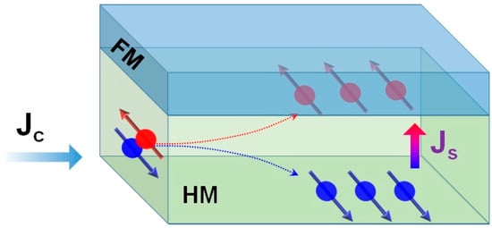
Figure 1.
Schematic of spin current transport in heavy metal/ferromagnet system. Spins of opposite sign (represented by red and blue dots) in the originally unpolarized current Jc are separated by the spin Hall effect in the heavy metal layer. The spins represented by red dots are immediately adjacent to the ferromagnetic layer and can thus interact with its magnetization [22].
2.3.3. Optical Spin Transfer
- Principles and Mechanisms
An important phenomenon that merges both the fields of optics and spintronics, optical spin transferring provides a means of controlling magnetization dynamics at extremely short timescales. Angular momentum is transferred from light to a material’s spin system during the operation. Circularly polarized light, which can cause spin-polarized photo-carriers in a material, usually starts this transfer. The material’s magnetic state can then change as a result of these photo-carriers transferring their spin angular momentum to the magnetization. The interplay between photo-carrier spin and a material’s magnetic moments is the main process of optical spin transfer. Because of optical selection principles, absorbed circularly polarized light produces spin-polarized carriers.
Recent tests have demonstrated the viability of optical spin transfer in a wide range of materials. When driven with circularly polarized laser pulses, (Ga, Mn), as ferromagnetic semiconductors, show coherent spin precession [23]. The optical spin-transfer torque causes this precession by aligning the photocarrier spin with the magnetization of the material. One of the most noticeable aspects of optical spin transfer is its quick dynamics. It is one of the fastest approaches for changing magnetism, with timescales ranging from femtoseconds to attoseconds. This makes it a viable solution for future data storage and spintronic devices that necessitate rapid manipulation of magnetic states.
The ability to manipulate magnetization dynamics with light opens up new avenues for ultrafast spintronic devices [24]. High-speed memory devices, adjustable oscillators, and spintronic circuit components are among the potential uses. The rapid nature of optical spin transfer could result in considerable improvements in data processing speed and energy efficiency. In the field of optical communication, optical spin transfer can be used to modulate signals quickly, potentially boosting data transmission rates. This approach has also shown promise in quantum computing applications, which require precise spin-state control to represent quantum bits (qubits) [12]. The sensitivity of optical spin-transfer techniques can be exploited to develop better magnetic sensors for a wide range of applications, including medical imaging and environmental monitoring. These sensors may offer more precision and responsiveness than conventional magnetic-sensing technology [25].
- Challenges and Limitations
Despite its potential, experimental detection and control of optical spin transfer are difficult. Accessing the element-specific transient density of states at the Fermi energy is critical for monitoring the process, which necessitates complex experimental setups such as time-resolved photoelectron spectroscopy [26]. One of the primary challenges in optical spin transfer is achieving precise control of spin states, which requires sophisticated laser systems and a deep understanding of light–matter interactions. The complexity of optical techniques, involving intricate interactions between light and magnetic materials, necessitates precise control over parameters such as light polarization and intensity. This complexity can make experimental setups challenging and costly. Efficiency and control pose significant challenges in optical spin transfer. Achieving efficient spin transfer with optical methods requires high precision in controlling the optical parameters and understanding the underlying physical mechanisms. This includes managing the effects of spin–orbit coupling and exchange interactions. Measurement and detection at the nanoscale present another hurdle. Detecting and measuring the effects of optical spin transfer at such small scales is challenging due to the minute magnitudes of the changes involved. Advanced techniques and sensitive equipment are necessary to accurately capture these effects. Scalability remains a significant challenge for practical applications. Scaling optical spin-transfer techniques for use in memory devices or logic circuits requires overcoming challenges related to the integration of optical components with electronic systems.
2.4. Spin–Orbit Torque
2.4.1. Origins and Mechanisms
A key concept in spintronics is spin–orbit torque (SOT), which offers a novel way for influencing a material’s magnetic states via electric currents [27]. The origins of SOT are deeply rooted in the spin–orbit interaction (SOI), an elementary phenomenon in quantum mechanics that results from the interaction of an electron’s orbital motion around an atomic nucleus with its spin. The Hamiltonian is a mathematical description of the spin–orbit interaction [28]:
where λ is the spin–orbit coupling constant, L is the orbital angular momentum, and S is the spin angular momentum. This equation shows that an electron’s energy is determined by the relative orientation of its spin and orbital angular momentum. Spin–orbit torque is largely produced by two mechanisms: the spin Hall effect (SHE) and the Rashba–Edelstein effect [29,30]. The spin Hall effect plays an important role in materials with significant spin–orbit coupling, such as heavy metals like platinum and tantalum. When an electric current flows through these materials, electrons scatter off impurities and lattice flaws, resulting in a spin current perpendicular to the charge current. This phenomenon is caused by the SHE, in which electrons with opposing spins deflect in opposite directions, resulting in a transverse spin current.
HSOI = λLS
The Rashba–Edelstein effect occurs at interfaces with broken inversion symmetry. The Rashba effect occurs when an electric current travels through such a contact, resulting in a non-equilibrium spin density. This spin density behaves like an effective magnetic field, known as the Rashba field, exerting a torque on magnetization.
Figure 2 shows how Rashba (SIA) and Dresselhaus (BIA + IIA) effects interact in quantum wells (QWs), specifically in zincblende-based QWs [31]. In these structures, the symmetry and asymmetry affect the strength of spin–orbit coupling. When symmetries change (e.g., from D2d to C2v), the Rashba effect can become comparable to or dominate over the Dresselhaus effect. The competition between these terms is analyzed through energy plots and spin orientations in figures. Nonlinear photocurrent spectroscopy is used to identify these contributions.
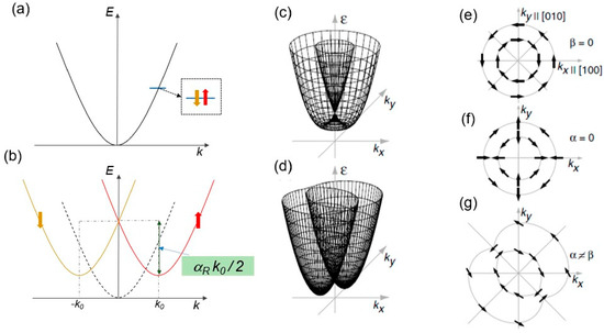
Figure 2.
Description of the Rashba effect. (a) Parabolic conduction band (CB) with spin-up and spin-down electrons occupying the same energy state, and the CB minimum is at momentum k = 0. (b) The CB is split by the Rashba effect, by k = k0 corresponding to an energy shift (αR k0/2) due to Rashba spin–orbit coupling (SOC) strength (αR); one band with spin-up (with minimum at k0), the other with spin-down (with minimum at −k0). (c–g) Schematics of 2D band structure with wave vector k-linear terms for C2v symmetry for different relative strengths of structural- and bulk-inversion asymmetry (SIA and BIA). (c) The distribution of spin orientations on the 2D Fermi surface is shown for the case of only Rashba or Dresselhaus SOC alone, while (d) shows the case of coexistence. (e,f) Two-dimensional plots for the Rashba SIA (α) and the Dresselhaus BIA (β), respectively (arrows indicate the spin orientations); note that spin directions are opposite from +kx to −ky (same in ±ky), in either case. While the spin orientation is always tangential in the case of SIA, it is perpendicular in the case of BIA at ±kx and ±ky and tangential otherwise. (g) Two-dimensional plot of the coexistence case of (d) [31].
2.4.2. Types of Spin–Orbit Torque
The two components that constitute SOT are damping-like and field-like torques.
- Damping-Like SOT: This torque is predominantly generated by the SHE and is useful for magnetization switching and domain wall motion. It is particularly well suited for memory applications such as magnetic random-access memory (MRAM) [28].
- Field-like SOT: Field-like SOT, which originates from the Rashba–Edelstein phenomenon, aids in precessional dynamics and improves overall magnetization control [32].
The development of spintronic devices is significantly impacted by SOT. It provides a promising technique for electrically manipulating magnetization dynamics in nanoscale heterostructures, which is critical to the development of next-generation memory and logic devices. The application of SOT is particularly valuable in the field of magnetic random-access memory (MRAM). It allows for independent reading and writing paths, extending memory longevity and improving operational performance. The ability to efficiently change magnetization states without the use of an external magnetic field is a significant advantage of SOT-based memory technology. With its rapid writing capabilities and minimal power usage, SOT-MRAM stands out as a promising memory application [33]. It provides non-volatility, which is crucial for data preservation in the absence of electricity.
The ability of SOTs to function at terahertz frequencies opens the door to ultrafast devices that are faster and more energy efficient than present technology. This feature makes SOT-based devices ideal for high-frequency applications in telecommunications and signal processing. Despite the potential applications of spin–orbit torque, a number of problems and limits prevent its full implementation in practical applications.
- Materials Selection and Efficiency: Identifying materials with high spin Hall angles and strong electrical conductivity is critical for successful SOT applications. While materials such as heavy metals, oxides, and topological insulators have been discovered, obtaining high SOT efficiency and electrical conductivity remains difficult.
- Symmetry and Strain Engineering: Because of the mirror symmetry of popular spin-source materials, it is difficult to achieve deterministic field-free switching of perpendicular magnetization. Strain engineering and symmetry breaking are being investigated as potential solutions to this constraint.
- Ferromagnet-Induced SOT: The invention of ferromagnet-induced SOT, which combines exchange and spin–orbit interactions, opens up new possibilities, but it also necessitates precise control over the generated spin direction and magnetization [34].
2.4.3. Technical Challenges
- Field-Free Switching: Most SOT applications require an external magnetic field for deterministic switching, limiting the materials and topologies that can be used. Techniques like symmetry breaking and unconventional SOT are being researched to enable field-free switching.
- Device Integration: Differences in material qualities and fabrication procedures make it difficult to integrate SOT materials into existing semiconductor technology. Commercial applications require device compatibility and reliability.
2.5. Comparison of Optical Spin Transfer and Other Spin-Manipulation Techniques
Comparing optical spin transfer to other spin-manipulation methods, especially STT and SOT, is crucial to understanding its importance.
2.5.1. Speed and Efficiency
One of the quickest methods for modifying spins is optical spin transfer, which works on femtosecond timeframes. Because of this, it is very effective for quick spin dynamics, which is essential for applications that need to analyze data quickly. In contrast, STT and SOT typically function on slower timelines despite their effectiveness. Energy dissipation may result from the constant current needed for STT, in particular. Because SOT does not need a magnetic field and can operate more quickly than STT, it uses less energy [20]. But in terms of speed, it still falls short of optical approaches. The ultrafast nature of optical spin transfer could lead to significant advancements in data-processing speeds and energy efficiency.
2.5.2. Control and Precision
Although optical techniques are faster, they necessitate exact control over laser parameters, which can be difficult to accomplish technically. Effective spin transfer and comprehension of the underlying physical mechanisms, such as controlling the effects of exchange contacts and spin–orbit coupling, require this degree of control. In contrast, STT and SOT depend on electrical currents, which are easier to manage and incorporate into already-existing electronic systems. This makes them easier to use in modern technologies, especially in memory applications where non-volatility and energy efficiency are key considerations.
2.5.3. Applications
Optical spin transfer is particularly promising for applications requiring rapid spin dynamics, such as ultrafast data-storage technologies and high-speed optical communication systems. It also holds potential for quantum computing applications, where the precise control of spin states is crucial. Spin-transfer torque is widely used in magnetic random-access memory (MRAM) and other spintronic devices where non-volatile memory is crucial. Meanwhile, SOT is being explored for future memory and logic technologies because it allows separate reading and writing paths and offers lower power consumption [21].
2.5.4. Challenges
Every method has a unique set of difficulties. The biggest challenge in optical spin transfer is precise control of spin states, which calls for advanced laser systems and extensive knowledge of light–matter interactions. There are also further difficulties in scaling optical spin-transfer methods for real-world use. Scalability and energy efficiency are issues for STT, particularly as device sizes decrease. Despite its potential, SOT still faces issues, including integrating materials into current semiconductor technology and attaining deterministic field-free switching. The technique ultimately depends on the particular needs of the application, such as speed, energy efficiency, and ease of implementation, even though optical spin transfer has significant speed and efficiency advantages that make it a compelling choice for future spintronic applications.
2.6. Future Prospects and Research Directions
The field of spintronics, particularly optical spin transfer and SOT, is poised for significant advancements. As research progresses, these technologies could revolutionize the way we approach data storage and processing, paving the way for more efficient and powerful electronic devices.
3. Applications and Advancements
Through its ability to precisely regulate spin states via light-induced angular momentum transfer, optical spin-transfer technology enables the controlled manipulation of spin currents in nanoscale devices, offering a promising pathway to enhance the speed, efficiency, and parallelism of mathematical calculation systems. Recent advancements in hybrid opto-electrical excitation of spin-transfer torque nano-oscillators (STNOs) using vertical-cavity surface-emitting lasers (VCSELs) have demonstrated how localized optical control can effectively modulate spin dynamics in nanoscale devices [35]. Moreover, the development of spin–orbit torque (SOT)-based devices has opened new avenues for manipulating spin currents through spin Hall and Rashba–Edelstein effects, with comprehensive device and architectural roadmaps detailing their potential applications [20,36]. Future research will focus on advanced device architectures capable of optimizing both spin transmission and SOT effects. Potential innovations include multifunctional devices combining memory and logic operations [37], three-dimensional spintronic structures [38,39], and neuromechanical computational systems [40,41], offering new paradigms for efficient, high-speed, and adaptive computing [42,43].
In addition, the development of devices that can function in the field of Terahertz, valuing the ultrafast optical transfer and SOT characteristics, could signal notable advancements in applications of different frequencies, such as ultrafast memory, high-speed optical communications, and sophisticated detection technologies. It is crucial to overcome certain obstacles for these technologies to become widely applicable, such as selecting optimal materials, integrating components effectively, and refining experimental methods. Therefore, it will be necessary to increase the scalability of optical spin transfer techniques, develop more effective methods for producing and detecting spin currents, and adapt materials compatible with SOT to current semiconductor technology.
3.1. Material Platforms
Various materials are being explored for their opto-spintronics potential based on their ability to interact with light and exhibit spin-related effects, such as spin–orbit coupling [44,45], spin-polarized currents [46], and magnetization manipulation via optical means [47]. Among these materials, diluted magnetic semiconductors are ideal for observing optical spin–torque phenomena due to their strong exchange interactions [48]. Due to their intrinsic magnetization, ferromagnetic materials like Fe used in devices like MRAM and spin injectors, Co used in spin valves and magnetic tunnel junctions (MTJs), as well as spin-polarized light-emitting diodes (spin-LEDs), and Ni used in magnetic sensors due to its high permeability, NiFe—a combination of nickel and iron permalloy widely used for its high permeability and low coercivity, or Rare-Earth Ferromagnets (e.g., Dysprosium, Terbium) with strong magnetic anisotropy, play a key role for STT and SOT effects in opto-spintronics. There have been reports of research on the creation of new diluted magnetic semiconductor materials, particularly bulk polycrystalline MnGexSby doped with Co or Fe [49]. Analysis was done on their electrical, magnetic, and structural characteristics. A recent paper published by Gish et.al. [50] examines the long-term use of van der Waals magnetic materials in optoelectronic and spintronic applications due to their sensitivity to external stimuli, highlighting potential applications in magnetics, neuromagnetic computation, and neural memory. Furthermore, 2D materials like MoS2, WS2, and WSe2 that have special qualities, including a high surface-to-volume ratio and improved spin–orbit coupling, are becoming more and more popular because of their direct bandgap and strong spin–orbit coupling, which makes them perfect for optical spin manipulation [51,52]. These transition metal dichalcogenides (TMDCs) are employed in opto-spintronics for light-induced spin production and are capable of hosting spin-polarized states.
These materials have inherent spin-polarized states due to their topological properties and are key to optical spin–orbit torque. The topological insulators (TI), including Bi2Se3 and Bi2Te3, possess spin-polarized surface states that exhibit strong spin-momentum locking, which can be used to induce spin-polarized currents when illuminated with light, offering potential for opto-spintronics applications [53,54]. Also, the heavy-metal alloys (e.g., Pt/Co, Ta/Co) exploit the large spin–orbit coupling in heavy metals like platinum (Pt) or tantalum (Ta), in combination with ferromagnetic layers (e.g., Co or Fe), to achieve optical spin manipulation through spin–orbit torques [55]. Another important class includes materials with strong spin–orbit coupling, and one of the widely used materials in spintronic heterostructures to control magnetization via SOT is Pt, due to its high spin–orbit coupling strength. Similar to platinum, W has a large spin–orbit coupling, making it suitable for SOT-based applications and for spin–polarized current generation in hybrid spintronic devices. Organic semiconductors (e.g., polycrystalline organic semiconductors) and hybrid materials (e.g., Perovskite-like CH3NH3PbI3) are increasingly explored for spintronic applications due to their flexibility, ease of fabrication, and integration with other devices [56].
Antiferromagnetic materials, though traditionally overlooked due to their lack of net magnetization, exhibit inherently faster spin dynamics and resilience to external magnetic disturbances, which are essential for ultrafast and stable spintronic devices. Kimel et al. [57] demonstrated that femtosecond laser pulses can be used to directly control the terahertz spin dynamics in an antiferromagnet (NiO), marking a major milestone in light-induced spin manipulation. This work opened the door for ultrafast, energy-efficient, and robust magnetic switching in antiferromagnetic materials, positioning them as key contenders for next-generation spintronic and quantum technologies.
3.2. Quantum Information Processing
Quantum information processing (QIP) relies on the precise control and manipulation of quantum bits (qubits), which may be based on electron spins, nuclear spins, or photonic modes. Optical photons are particularly suited for transmitting quantum information over long distances due to their high speed and low loss, while spin systems offer long coherence times and stable local processing capabilities. A central challenge in QIP is the development of efficient interfaces between stationary qubits (spins) and flying qubits (photons). The optical–spin interaction enables this functionality by allowing coherent transfer of quantum states between these physical carriers.
Four essential mechanisms are involved in the optical–spin interaction in quantum information processing (QIP):
- Optical Initialization: Qubits are prepared in specific states via the excitation of spin-selective transitions in systems such as donor atoms, color centers, and quantum dots by circularly polarized light.
- Coherent Optical Control: Often in nanophotonic systems, laser-driven Raman transitions, optical Stark shifts, and cavity-enhanced coupling allow for precise spin-state manipulation for single-qubit rotations and entangling gates.
- Spin–Photon Entanglement: Resonant optical transitions enable distributed entanglement for quantum networks by entangling a spin with the polarization, frequency, or time-bin of a photon through radiative decay or cavity-modified emission.
- Optical Readout: Using variations in fluorescence or emission lifetimes, spin-dependent photoluminescence, or cavity transmission is used to measure final spin states.
Recent advances in material science, cavity quantum electrodynamics (cQED), and nanophotonics have significantly enhanced the efficiency and scalability of these interfaces [58,59,60,61,62].
Researchers used a shared photonic mode in a superconducting microwave cavity to show coherent coupling between two geographically separated electron spins in a historic experiment [63]. This was accomplished by utilizing the exchange of virtual photons to mediate an efficient spin–spin interaction and positioning each spin qubit at distinct nodes of a top-notch superconducting resonator. The system’s coherence duration and coupling strength were adequate to detect entanglement dynamics and coherent oscillations between the far-flung qubits. The foundation for distributed quantum information processing is laid by this photon-mediated interaction technique, which allows modular quantum processors to be coupled via photonic channels. The spin qubit directly changes the resonance frequency of a superconducting cavity in silicon-based quantum dots, demonstrating a novel coupling regime [64]. Photon-exchange processes are not involved in this longitudinal coupling, in contrast to the traditional transverse (Jaynes–Cummings) interaction. Rather, a static shift in the cavity frequency occurs when the qubit is in a specific state. There are various benefits to this kind of contact, such as increased speed of qubit readout, decoherence suppression due to cavity photon loss, and adaptability to high-fidelity, quick gate operations. A viable path for combining semiconductor qubits with superconducting quantum circuits in a scalable and noise-resistant architecture is established by the experimental realization of this regime in silicon.
The spin–orbit interaction phenomena were used to create a unique spin–photon interface in silicon, furthering the integration of spin-based qubits into scalable quantum photonic devices [65]. By engineering the confinement and electronic properties of silicon nanostructures, researchers have achieved an effective coupling between localized electron spins and photonic modes without requiring external magnetic fields. This magnetic-free architecture improves compatibility with Complementary Metal-Oxide-Semiconductor (CMOS)-compatible manufacturing techniques and makes it easier to integrate spin qubits with current silicon photonic platforms.
Researchers created entanglement between a single photon and a localized electron spin in silicon carbide (SiC) in a noteworthy illustration of optically mediated spin–photon entanglement [66]. SiC’s broad bandgap, sophisticated production methods, and potential for room-temperature operation make it an especially alluring material platform. Resonant optical excitation was used in the work to create entangled spin–photon pairs after optically correcting a color center defect in SiC. This finding supports SiC’s position as a viable option for real-world quantum information systems by confirming that it can be used for distributed entanglement generation and scalable quantum networks.
3.3. Energy Harvesting and Sensing
In this area, optical–spin interactions play a pivotal role in enhancing energy conversion and sensing functionality. For instance, non-thermal light-induced magnetization switching, such as the inverse Faraday effect, enables ultrafast and energy-efficient control of spin states without significant thermal dissipation. Through novel processes that take advantage of electron spin and light interactions to increase functionality and efficiency, opto-spintronics improve energy harvesting. There are several instances that can be described in depth to show different principles or applications related to the use of opto-spintronics in energy harvesting. As demonstrated by spin-based perovskite solar cells, where spin-polarized carriers improve light-to-electricity conversion by reducing recombination losses, spin–photovoltaic cells use electron spin to minimize energy losses during charge transport. Spin–photovoltaic effects in atomically thin CrI3 van der Waals heterostructures were investigated by Song et al. [67]. In CrI3, a huge photo-magneto current phenomenon and different responses of the photocurrent to the spin configurations were seen. The emergent interaction between the spin photocurrent and the underlying excitons, inherent magnetic order, photon energy, and helicity was demonstrated by their circular polarization-resolved absorption studies in conjunction with their helicity-dependent photocurrent. They used the intrinsic magnetic order in few-layer CrI3 to demonstrate a proof-of-concept 2D spin–photovoltaic device. This study also established an atomically thin CrI3 as an archetypal 2D magnet for studying photocurrent generation in a vertical junction device. This device structure showed promise for possible uses in magnetic sensing and data storage and may be modified using additional 2D magnets with different magnetic order and coercive fields, such as CrBr3, CrCl3, and CrSBr. Under unpolarized white light, Savadkoohi et al. [68] demonstrated for the first time the electronic spin-dependent solar cell effect on a single-molecule magnet (SMM)-transformed magnetic tunnel junction (MTJ). Where the physical distance between the electrodes was less than the length of the SMM spin channels that needed to be bridged, cross-junction-shaped MTJs with two exposed junction edges were produced using CoFeB on both sides of the MgO tunnel barrier. Long-range magnetic resonance was produced by bridging the gap between the two CoFeB electrodes along the exposed edges of the insulating barrier.
The SMM used was a hexanuclear [Mn6(μ3-O)2(H2N-sao)6(6-atha)2(EtOH)6] complex with thiol end groups that bonded with the metal films. The MTJ with the SMM exhibited a solar cell effect, yielding an open-circuit voltage of approximately 80 mV and a saturation current of around 10 mA/cm2 under one sun radiation. Kelvin Probe Atomic Force Microscopy (KPAFM) studies provided direct evidence that the SMM transformed the electronic properties of the MTJ electrodes over an area several thousand times larger than the molecular junctions at room temperature. The spin Seebeck Effect (SSE) is a remarkable discovery in the field of spintronics, which investigates the spin of electrons as a basis for next-generation electronic devices. Since its identification in 2008 [69], the SSE has gained attention for its potential in advancing energy conversion and information processing technologies. By using optical stimulation to create temperature gradients in magnetic materials for thermoelectric harvesting, spin Seebeck effect devices turn thermal energy from temperature gradients into spin currents, which are subsequently converted into electrical energy via spin–charge coupling. The SSE has been found in a wide range of materials, such as paramagnets, ferromagnets, and antiferromagnets, demonstrating its versatility and general applicability for a range of applications. The contacts between magnetic and nonmagnetic metals have a significant impact on the effect. The inverse spin Hall effect at these interfaces transforms spin currents produced in the magnetic material into detectable electrical signals, highlighting the need for interface optimization. Temperature gradients and inherent material characteristics affect the SSE’s strength, which makes it particularly pertinent for waste heat-recovery applications. For instance, the Pt/Y3Fe5O12 (YIG) tests described in [70] showed that the anomalous Nernst effect (ANE) and LSSE can be distinguished from one another. This indicates that the thermoelectric voltage in Pt/YIG is mostly caused by LSSE, with a very small contribution from ANE. Additionally, measurements in Au/YIG (free from proximity ferromagnetism) verified that LSSE is different from proximity ANE and intrinsic. Additionally, ref. [71] is another intriguing work that suggests an effective way to increase the spin Seebeck effect (SSE) signal by decreasing the exchange interaction (Jex) in a ferromagnet’s (FM) hotter area.
By increasing the magnon heat current, this lowering raises the magnon temperature (Tme) and strengthens the SSE signal. Furthermore, as Jex is crucial in defining magnon density through its effect on the Curie temperature, increasing the gradient of the magnon chemical potential (∇μm) under a specific temperature gradient further amplifies the SSE. The magnon temperature model and the magnon drift-diffusion model are two theoretical frameworks for explaining the SSE that was examined in that paper. For clarity, these mechanisms are examined independently, even though they might coexist. Moreover, ref. [72] reports a significantly enhanced longitudinal spin Seebeck coefficient in the Au/polycrystalline Y3Fe5O12 (YIG) system, which was achieved using high-density surface magnetic moments, and improved surface finishing of YIG pellets. In the Au/YIG system, the LSSE voltage increases linearly with the temperature gradient (ΔT) and varies sinusoidally with the external magnetic field (θ). The LSSE coefficients were 0.163 μV/K and 0.181 μV/K for ΔT = 11 K and 19 K, which is 11.1 times greater than the previous value of 0.016 μV/K. The density of the surface moment and quality above the surface of YIG particles are the main indicators of ubiquity. When discussing the magnetoelectric generators as a condition of light, it is well known that they use light to manipulate magnetic fields and facilitate energy exchange.
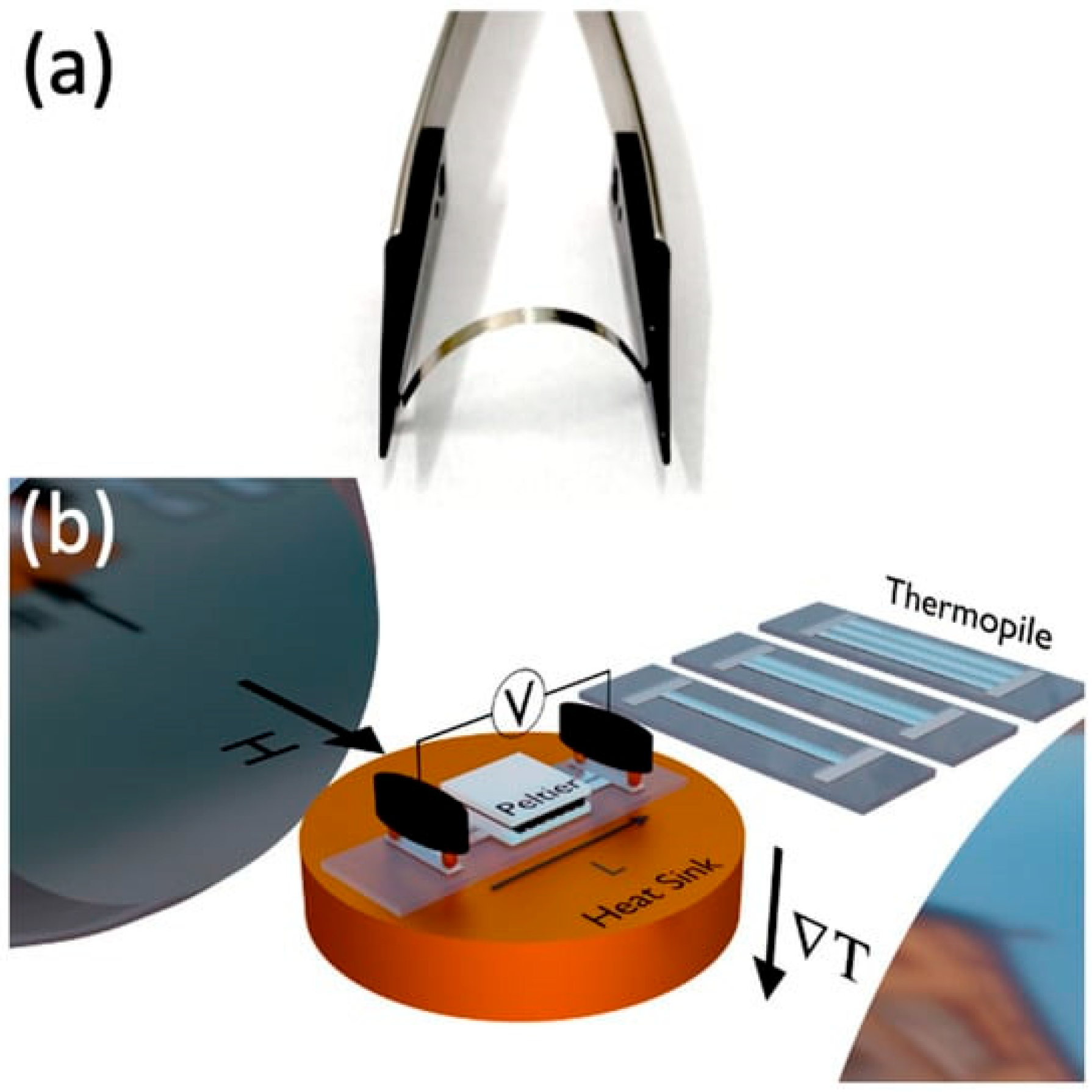
Thermoelectric voltage conversion in bare Co-rich ribbons and ribbon/Pt heterostructures was used to study the thermoelectrical phenomenon in [73], with particular attention to the longitudinal spin Seebeck effect (LSSE) and the anomalous Nernst effect (ANE) (Figure 3).

Figure 3.
(a) Image of bare Fe3Co67Cr3Si15B12 flexible ribbon. (b) Schematic representation of the thermoelectric experimental setup. In particular, the arrow characterizing the field corresponds to the direction labelled as φH = 90° [73].
It was found that the ferromagnetic amorphous ribbon’s (Figure 3a) magnetic characteristics remained unchanged after a thin layer of Pt was deposited on its surface. The magnetization curves for certain magnetic field orientations were reflected in the thermoelectric data, with specific situations exhibiting the highest voltage. The Pt layer protected against surface oxidation, raised the thermoelectric voltage, and improved spin-to-charge conversion. Furthermore, by lowering system resistance, thermopiles of Co-rich ribbon/Pt heterostructures arranged in parallel (Figure 3b) greatly increased thermoelectric current [73].
In 2022, a neural collector that can capture multidirectional vibrational energy on a wide band was reported [74]. Magnetic interactions extend the harvesting frequency range, and the results validate system efficiency with a band length extension of 5.2 Hz. Quantum dot spin systems leverage spin-based optoelectronic properties for ultra-compact and highly efficient energy harvesters, such as nanoscale devices that capture energy from ambient light with remarkable spectral sensitivity. For example, the integration of 2D magnets in quantum sensing has revolutionized precision, allowing for the quantum-level measurement of physical quantities like temperature and time. Sensors utilizing quantum phenomena such as spin-dependent transport have achieved exceptional accuracy in detecting magnetic fields and electromagnetic waves [75,76,77].
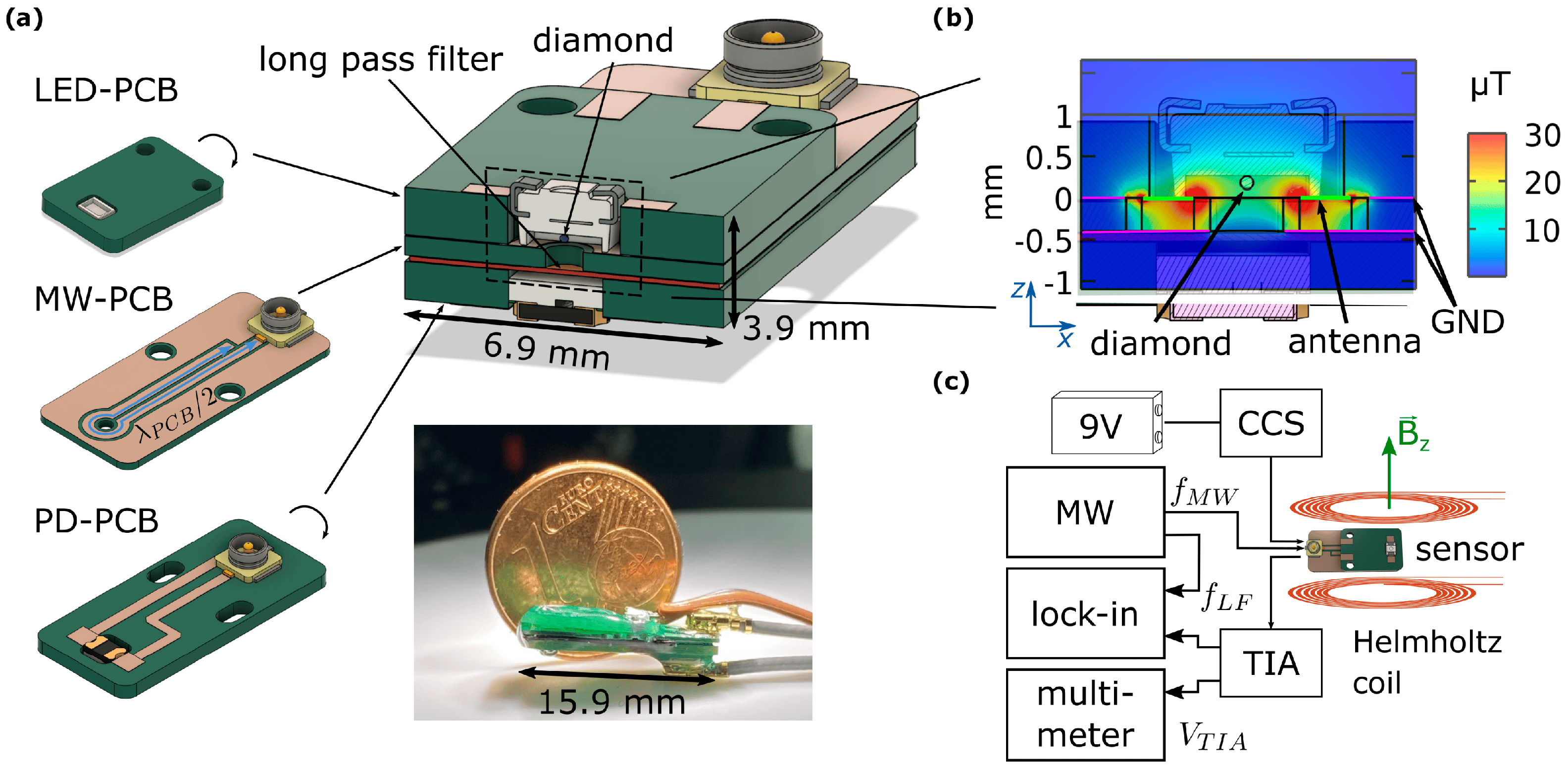
The sensor, illustrated in Figure 4a [75], consists of a stacked assembly of three PCBs fabricated using standard design rules. The first PCB hosts an LED and a diamond microcrystal (~170 μm, 2.5–3 ppm NV center concentration) fixed with optical adhesive, providing a strong fluorescence signal. The second PCB integrates a λ/2 microwave antenna, wound around a central hole to generate a homogeneous microwave field and allow fluorescence collection. A photodiode, mounted on the third PCB, detects the NV emission, filtered through a 622 nm long-pass filter. The antenna’s length is precisely tuned to the NV resonance frequency (2.87 GHz), ensuring a maximum magnetic field at the diamond position. The simulations conducted with COMSOL Multiphysics have confirmed efficient field confinement and uniformity, with minimal angular deviation in the diamond region, which is consistent with established NV sensor geometries. While NV centers in diamonds have shown promise as quantum sensors, challenges in integrating diamond components into devices have led to the exploration of defect states in 2D materials like h-BN and transition metal dichalcogenides [75]. This approach offers new opportunities for characterizing nanoscale 2D magnetism, as demonstrated by the NV center’s ability to probe static magnetism in 2D materials with nanoscale resolution.

Figure 4.
(a) Sensor setup containing light-emitting diode-printed circuit board (LED-PCB), microwave (MW) antenna structure (MW-PCB), and the PCB to mount the photodiode (PD-PCB), as well as the 100 μm-thick filter foil between MW-PCB and PD-PCB. The overall size is (6.9 × 3.65 × 15.9) mm3. (b) Simulation of the field distribution inside the sensor at 10 dBm microwave power. (c) Electronic block diagram. A 9 V battery feeds a lab-built constant current source for 30 mA LED current. The microwave source generates a frequency-modulated microwave whose low-frequency is used as the demodulation frequency for the lock-in amplifier (LIA). The photocurrent is fed to a lab-built transimpedance amplifier (TIA), which provides input voltage for the LIA and a multimeter [75].
3.4. 2D Magnets in Opto-Spintronics
Two-dimensional (2D) magnets are materials whose magnetism is limited to one or a few atomic layers [78] that are particularly suited for opto-spintronics due to their atomic-scale thickness and strong light-matter coupling. Materials with magnetism restricted to one or a few atomic layers are known as two-dimensional (2D) magnets. Van der Waals minerals include, for example, CrI3, CrGe2Te6, and FeGeTe2. These materials’ adjustable magnetic characteristics and compatibility with other 2D materials, such as graphene or transition metal dichalcogenides (TMDs), have generated interest. Two-dimensional magnets can maintain their magnetic characteristics even when only one atomic layer is around 0.8 nm thick. They generate quantum events that are not observed in their bulk counterparts due to their remarkable magnetic anisotropy. They differ from conventional bulk magnetic materials due to their unique characteristics, which include quantum confinement, which confines carriers to a 2D plane, and mechanical flexibility due to their ultrathin structure. These materials exhibit improved electrical, thermal, and optical sensitivity [79], making them highly responsive to external stimuli such as electric fields, laser manipulation, chemical changes, and mechanical strain. Furthermore, their electronic and magnetic properties can be precisely adjusted through external factors like electric gating [80] and strain [81]. These unique attributes pave the way for the use of 2D magnets in ultracompact devices.
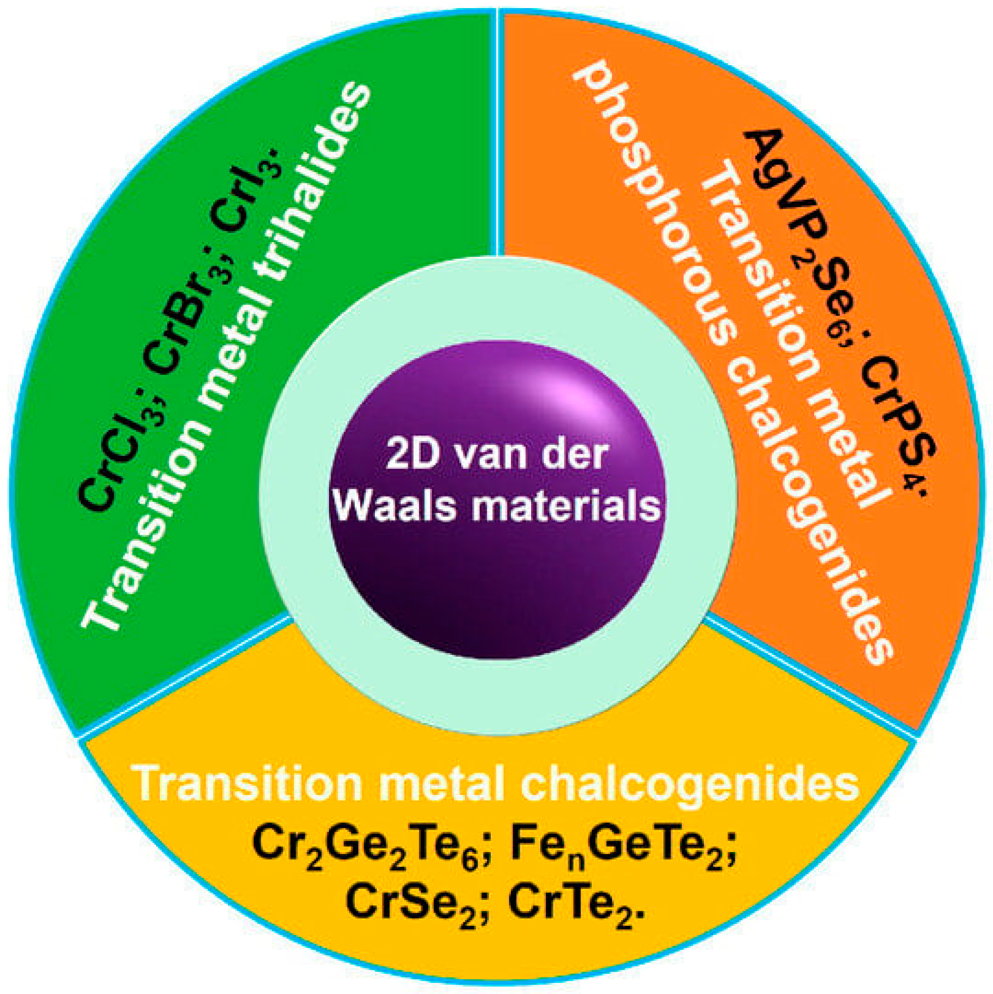
Figure 5 highlights recent progress in the strain engineering of intrinsic ferromagnetism in 2D van der Waals materials. The focus is on Cr- and Fe-based systems, including transition metal trihalides, chalcogenides, and phosphorus chalcogenides, emphasizing both current challenges and future opportunities in spintronics and straintronics [81].

Figure 5.
The three different kinds of 2D van der Waals materials with intrinsic long-range ferromagnetic order [81].
The 2D ferromagnet Cr2Ge2Te6 (CGT), which is extremely resistive below its Curie temperature, made it more difficult to examine its magnetism by electrical transport, according to a study by Lohmann et al. [82]. On thin (<50 nm) CGT flakes, heterostructures, including Pt, demonstrated a distinct anomalous Hall effect (AHE) in 5 nm-thick Pt, with hysteresis loops continuing up to about 60 K, which is the Curie temperature of CGT. Low-temperature magnetic force microscopy verified the AHE loop indication of magnetic domain development. These results demonstrated that CGT affects the magnetization of the Pt layer. The observed AHE may be explained by the induced ferromagnetism in Pt, according to calculations using density functional theory. This provides a novel approach to the study of magnetism in 2D insulating ferromagnets and may have applications in monolayer devices. Two-dimensional magnets demonstrate magneto-optical phenomena like the Faraday or Kerr effect, which are vital for optical data storage and spin manipulation. The practical applications of conventional materials are limited by their weak magneto-optical (MO) signals. Recent developments concentrate on using localized surface plasmon resonances (LSPR) to hybridize these materials with noble metal nanostructures. To improve the quality factor and the polar magneto-optical Kerr effect (PMOKE), a new magneto-optical surface plasmon resonance (MOSPR) structure utilizing Au bowtie arrays was created [83]. The Au bowties’ dimensions and shape were tuned by finite-element-method (FEM) simulations, which produced notable LSPR effects. This resulted in a significant improvement in the quality factor and a 3255-fold amplification of the PMOKE signal, providing a viable avenue for high-performance MO devices.
3.5. Room-Temperature Control of Molecular Spins
Recent advances have demonstrated the feasibility of optically controlled spin states in molecular systems operating at room temperature. Thermal fluctuations make it difficult to manage molecular spins at normal temperature because molecules are always vibrating and colliding, which can upset spin states. Furthermore, it is more difficult to retain control because molecules’ spin states have a tendency to relax (or lose their coherence) over time, and higher temperatures accelerate this process. Decoherence or loss of quantum information may result from interactions between spins and their environment, including adjacent nuclei or electrons.
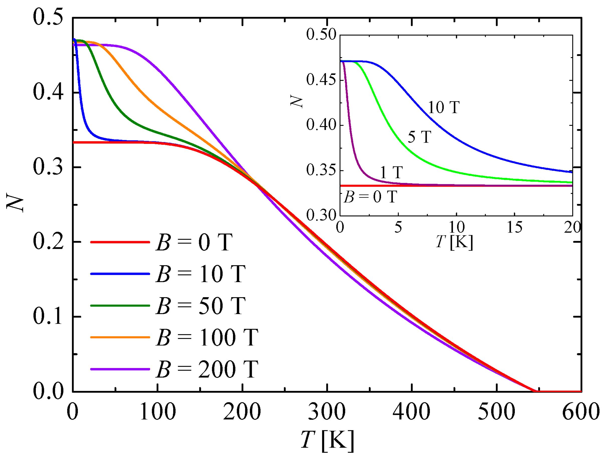
However, recent work published in high-impact publications demonstrates that significant progress has been made thus far in the management of molecule spins at room temperature [84]. This development is critical to the practical implementation of optospintronics. The room-temperature, all-2D van der Waals (vdW) spin-valve device disclosed by Jin et al. [85] was based on a (FM) 2D crystal and demonstrated a considerable spin-valve effect that was strongly dependent on the thickness of the MoS2 spacer. The magnetoresistance (MR) of the device was 15.89% at 2.3 K and 11.97% at 10 K, which is 4–30 times greater than that of spin valves made of Fe3GeTe2/MoS2/Fe3GeTe2 and standard NiFe/MoS2/NiFe. Importantly, the spin-valve effect remained at low working currents of 10 nA even at 300 K. In a study from 2023, calculations were used to examine the electrical and magnetic characteristics of MoS2 and WS2 quantum dots [86]. Unpaired electrons on the margins of these dots provide them a permanent spin. The spin can change from ferromagnetic to antiferromagnetic or nonmagnetic by applying a 2H passivation. At room temperature, these magnetic states remain constant. Their magnetic characteristics are diminished by edge sulphuration, and they become diamagnetic in WS2 dots when 2H passivation is added. Because sulphur atoms alter the energy levels, these semiconductors have energy gaps of around 3.3 eV, which decrease with edge passivation. Spintronic devices may benefit from the WS2 and MoS2 quantum dots’ tunable magnetic and electrical characteristics [86]. The molecular compound (Et3NH)[Ni(hfac)2L) preserves a considerable degree of thermal entanglement at room temperature, which only diminishes at 546 K, according to [87]. These results underline the central role of light in stabilizing and manipulating molecular spin states for functional spintronic applications. Figure 6 shows the temperature dependence of negativity in a mixed spin-(1/2,1) Heisenberg dimer modeled for (Et3NH)[Ni(hfac)2L]. At zero field, negativity decreases from = 1/3, vanishing near 546 K. Low magnetic fields (B ≲ 50 T) raise the zero-temperature negativity to = 2√3 ≈ 0.47, followed by a sharp thermal drop. This effect diminishes at higher fields, with noticeable field-induced reduction only above 200 T. The results highlight how temperature and magnetic field modulate quantum entanglement in such systems. This finding suggests that the material might be employed in quantum computing applications as a molecular qubit.

Figure 6.
Temperature variations of the negativity calculated at a few selected values of the external magnetic field for the mixed spin-(1/2,1) Heisenberg dimer provided by the Hamiltonian (1) with the parameter set J/kB = 505 K, grad = 2.005, and gNi = 2.275 (J/kB is the ratio of energy (Joules) to the Boltzmann constant (kB) and grad and gNi are two distinct g-factors, for a Radical or a system and nickel) adjusted to a theoretical modelling of the molecular complex (Et3NH)[Ni(hfac)2L]. The inset shows a detail from the low-temperature region, and it includes a few additional values of the small magnetic field [87].
4. Conclusions
In this review, we have demonstrated that opto-spintronics is an important field of research that studies materials that interact with light and spin systems in various solid-state materials. Diluted magnetic semiconductors, two-dimensional magnets, and molecular spin systems have been identified as particularly promising platforms for future applications in quantum computing, energy harvesting, and sensing technologies.
In our view, hybrid systems will be at the forefront of future breakthroughs, combining the fast spin dynamics of antiferromagnetic materials with the high optical tunability of two-dimensional materials that can be integrated directly into existing semiconductor platforms.
We believe that it is important to have clear material design strategies, such as strain engineering, defect manipulation, and interface tailoring, to achieve scalable, low-power, and ultrafast spin-based devices. Additionally, the exploration of organic–inorganic hybrid materials for flexible and tunable opto-spintronics presents an exciting frontier.
In the near future, we believe that opto-spintronics will transform modern technology by enabling devices that combine photonic control, spin manipulation, and energy efficiency. Addressing challenges such as robust room-temperature operation, deterministic spin control without magnetic fields, and seamless integration with classical electronics will define the next stage of innovation in this rapidly evolving field.
Author Contributions
Conceptualization, A.-M.F., A.-M.I., S.C., S.-M.I. and B.B.; methodology, A.-M.F., A.-M.I., S.C., S.-M.I. and B.B.; data curation, A.-M.F., A.-M.I., S.C., S.-M.I. and B.B.; writing—original draft preparation, A.-M.F., A.-M.I., S.C., S.-M.I. and B.B.; writing—review and editing, A.-M.F., A.-M.I., S.C., S.-M.I. and B.B.; visualization, A.-M.F., A.-M.I., S.C., S.-M.I. and B.B.; supervision, A.-M.F., A.-M.I., S.C., S.-M.I. and B.B. All authors have read and agreed to the published version of the manuscript.
Funding
This research received no external funding.
Institutional Review Board Statement
Not applicable.
Informed Consent Statement
Not applicable.
Data Availability Statement
Data are contained within the article.
Acknowledgments
Ana-Maria Florea (Raduta), Stefan Caramizoiu, Ana-Maria Iordache, Stefan-Marian Iordache, and Bogdan Bita were supported by the CORE Program, carried out with the support of MCID, project no. PN 23 05.
Conflicts of Interest
The authors declare no conflicts of interest.
References
- Fang, N.; Wu, C.; Zhang, Y.; Li, Z.; Zhou, Z. Perspectives: Light control of magnetism and device development. ACS Nano 2024, 18, 8600–8625. [Google Scholar] [CrossRef] [PubMed]
- Sierra, J.F.; Fabian, J.; Kawakami, R.K.; Roche, S.; Valenzuela, S.O. Van der Waals heterostructures for spintronics and opto-spintronics. Nat. Nanotechnol. 2021, 16, 856–868. [Google Scholar] [CrossRef]
- Chen, H.; Zhang, J.; Kan, D.; He, J.; Song, M.; Pang, J.; Wei, S.; Chen, K. The recent progress of Two-Dimensional Transition Metal Dichalcogenides and their phase transition. Crystals 2022, 12, 1381. [Google Scholar] [CrossRef]
- Jia, Z.; Zhao, M.; Chen, Q.; Tian, Y.; Liu, L.; Zhang, F.; Zhang, D.; Ji, Y.; Camargo, B.; Ye, K.; et al. Spintronic Devices upon 2D Magnetic Materials and Heterojunctions. ACS Nano 2025, 19, 9452–9483. [Google Scholar] [CrossRef] [PubMed]
- Xu, X.; Lou, Z.; Cheng, S.; Chow, P.C.; Koch, N.; Cheng, H.-M. Van der Waals organic/inorganic heterostructures in the two-dimensional limit. Chem 2021, 7, 2989–3026. [Google Scholar] [CrossRef]
- Meng, F.; Donnelly, C.; Skoric, L.; Hierro-Rodriguez, A.; Liao, J.-W.; Fernández-Pacheco, A. Fabrication of a 3D Nanomagnetic Circuit with Multi-Layered Materials for Applications in Spintronics. Micromachines 2021, 12, 859. [Google Scholar] [CrossRef] [PubMed]
- Rojas-Lopez, R.R.; Hendriks, F.; van der Wal, C.H.; Guimarães, P.S.S.; Guimarães, M.H.D. Charge dynamics in the 2D/3D semiconductor heterostructure WSe2/GaAs. Appl. Phys. Lett. 2024, 125, 132104. [Google Scholar] [CrossRef]
- Song, T.; Xu, X. The future of 2D spintronics. Nat. Rev. Electr. Eng. 2024, 1, 696–697. [Google Scholar] [CrossRef]
- Hu, X.-M.; Guo, Y.; Liu, B.-H.; Li, C.-F.; Guo, G.-C. Progress in quantum teleportation. Nat. Rev. Phys. 2023, 5, 339–353. [Google Scholar] [CrossRef]
- Guimarães, F.S.M.; Bouaziz, J.; Dias, M.d.S.; Lounis, S. Spin-orbit torques and their associated effective fields from gigahertz to terahertz. Commun. Phys. 2020, 3, 19. [Google Scholar] [CrossRef]
- Davies, C.S.; Kirilyuk, A. Epsilon-near-zero regime for ultrafast opto-spintronics. Npj Spintron. 2024, 2, 20. [Google Scholar] [CrossRef] [PubMed]
- Al-Qatatsheh, A.; Juodkazis, S.; Hameed, N. Bridging performance gaps: Exploring new classes of materials for future spintronics technological challenges. Adv. Quantum Technol. 2023, 6, 2300204. [Google Scholar] [CrossRef]
- Vernon, A.J.; Golat, S.; Rigouzzo, C.; Lim, E.A.; Rodríguez-Fortuño, F.J. A decomposition of light’s spin angular momentum density. Light Sci. Appl. 2024, 13, 160. [Google Scholar] [CrossRef] [PubMed]
- Darrigol, O. A Faradayan principle for selecting classical field theories. Int. Stud. Philos. Sci. 2007, 21, 35–55. [Google Scholar] [CrossRef]
- Seo, Y.; Kwon, K.-W. High-Density 1R/1W Dual-Port Spin-Transfer Torque MRAM. Micromachines 2022, 13, 2224. [Google Scholar] [CrossRef]
- Cai, H.; Kang, W.; Wang, Y.; Naviner, L.A.D.B.; Yang, J.; Zhao, W. High Performance MRAM with Spin-Transfer-Torque and Voltage-Controlled Magnetic Anisotropy Effects. Appl. Sci. 2017, 7, 929. [Google Scholar] [CrossRef]
- Dyakonov, M.I. Optical Orientation of Spins in Semiconductors. In Encyclopedia of Condensed Matter Physics; Elsevier: Amsterdam, The Netherlands, 2024; pp. 223–232. [Google Scholar] [CrossRef]
- Song, C.; Zhang, R.; Liao, L.; Zhou, Y.; Zhou, X.; Chen, R.; You, Y.; Chen, X.; Pan, F. Spin-orbit torques: Materials, mechanisms, performances, and potential applications. Prog. Mater. Sci. 2021, 118, 100761. [Google Scholar] [CrossRef]
- Mahfouzi, F.; Mishra, R.; Chang, P.-H.; Yang, H.; Kioussis, N. Microscopic origin of spin-orbit torque in ferromagnetic heterostructures: A first-principles approach. Phys. Rev. B 2020, 101, 060405. [Google Scholar] [CrossRef]
- Shao, Q.; Li, P.; Liu, L.; Yang, H.; Fukami, S.; Razavi, A.; Wu, H.; Wang, K.; Freimuth, F.; Mokrousov, Y.; et al. Roadmap of spin-orbit torques. arXiv 2021. [Google Scholar] [CrossRef]
- Ji, G.; Zhang, Y.; Chai, Y.; Nan, T. Recent progress on controlling spin-orbit torques by materials design. Npj Spintron. 2024, 2, 56. [Google Scholar] [CrossRef]
- Lee, S.; Liu, X.; Furdyna, J. Controlling magnetization in ferromagnetic semiconductors by Current-Induced Spin-Orbit torque. Materials 2025, 18, 271. [Google Scholar] [CrossRef]
- Němec, P.; Rozkotová, E.; Tesařová, N.; Trojánek, F.; De Ranieri, E.; Olejník, K.; Zemen, J.; Novák, V.; Cukr, M.; Malý, P.; et al. Experimental observation of the optical spin transfer torque. Nat. Phys. 2012, 8, 411–415. [Google Scholar] [CrossRef]
- Willems, F.; Schmising, C.v.K.; Strüber, C.; Schick, D.; Engel, D.W.; Dewhurst, J.K.; Elliott, P.; Sharma, S.; Eisebitt, S. Optical inter-site spin transfer probed by energy and spin-resolved transient absorption spectroscopy. Nat. Commun. 2020, 11, 871. [Google Scholar] [CrossRef] [PubMed]
- Leitao, D.C.; van Riel, F.J.F.; Rasly, M.; Araujo, P.D.R.; Salvador, M.; Paz, E.; Koopmans, B. Enhanced performance and functionality in spintronic sensors. Npj Spintron. 2024, 2, 54. [Google Scholar] [CrossRef]
- Aeschlimann, M.; Bange, J.P.; Bauer, M.; Bovensiepen, U.; Elmers, H.-J.; Fauster, T.; Gierster, L.; Höfer, U.; Huber, R.; Li, A.; et al. Time-resolved photoelectron spectroscopy at surfaces. Surf. Sci. 2024, 753, 122631. [Google Scholar] [CrossRef]
- Haney, P.M.; Stiles, M.D. Current-Induced torques in the presence of Spin-Orbit coupling. Phys. Rev. Lett. 2010, 105, 126602. [Google Scholar] [CrossRef]
- Spin Orbit torque. Intuitive Tutorials. Available online: https://intuitivetutorial.com/2024/08/05/harnessing-quantum-forces-the-microscopic-origins-of-spin-orbit-torque (accessed on 10 January 2025).
- Žutić, I.; Fabian, J.; Sarma, S.D. Spintronics: Fundamentals and applications. Rev. Mod. Phys. 2004, 76, 323–410. [Google Scholar] [CrossRef]
- Li, J.; Haney, P.M. Optical spin transfer and spin-orbit torques in thin-film ferromagnets. Phys. Rev. B 2017, 96, 054447. [Google Scholar] [CrossRef]
- Chen, J.; Koc, H.; Zhao, S.; Wang, K.; Chao, L.; Eginligil, M. Emerging nonlinear photocurrents in lead halide perovskites for spintronics. Materials 2024, 17, 1820. [Google Scholar] [CrossRef]
- Amin, V.P.; Haney, P.M.; Stiles, M.D. Interfacial spin–orbit torques. J. Appl. Phys. 2020, 128, 151101. [Google Scholar] [CrossRef]
- Seo, Y.; Kwon, K.-W. Ultra High-Density SOT-MRAM design for Last-Level On-Chip Cache Application. Electronics 2023, 12, 4223. [Google Scholar] [CrossRef]
- Kim, K.-W.; Park, B.-G.; Lee, K.-J. Spin current and spin-orbit torque induced by ferromagnets. Npj Spintron. 2024, 2, 8. [Google Scholar] [CrossRef]
- Oberbauer, F.; Winkel, T.J.; Böhnert, T.; Claro, M.S.; Benetti, L.; Çaha, I.; Francis, L.; Moradi, F.; Ferreira, R.; Münzenberg, M.; et al. Hybrid Opto-Electrical excitation of Spin-Transfer torque Nano-Oscillators for advanced computing. arXiv 2025. [Google Scholar] [CrossRef]
- Moradi, F.; Farkhani, H.; Zeinali, B.; Ghanatian, H.; Pelloux-Prayer, J.M.A.; Böhnert, T.; Zahedinejad, M.; Heidari, H.; Nabaei, V.; Ferreira, R.; et al. Spin-Orbit-Torque-based devices, circuits and architectures. arXiv 2019. [Google Scholar] [CrossRef]
- Lopez-Dominguez, V.; Shao, Y.; Amiri, P.K. Perspectives on field-free spin–orbit torque devices for memory and computing applications. J. Appl. Phys. 2023, 133, 040902. [Google Scholar] [CrossRef]
- Yang, Y.; Wang, J. Enhancing Unconventional Spin-Orbit Torque Efficiency: First numerical study on the influence of crystallographic texture and polycrystalline effects on Low-Symmetry materials. arXiv 2025. [Google Scholar] [CrossRef]
- Hu, G.; Xiang, B. Recent advances in Two-Dimensional Spintronics. Nanoscale Res. Lett. 2020, 15, 1–17. [Google Scholar] [CrossRef] [PubMed]
- Hu, H.; Wang, K.; Li, W.; Zuo, C.; Tang, R.; Dong, K. Spin–orbit torque-induced memristor in Ta/GdFeCo/Ta structures for neuromorphic computing. J. Magn. Magn. Mater. 2023, 589, 171582. [Google Scholar] [CrossRef]
- Kumar, D.; Maddu, R.; Chung, H.J.; Rahaman, H.; Jin, T.; Bhatti, S.; Ter Lim, S.; Sbiaa, R.; Piramanayagam, S.N. Emulation of neuron and synaptic functions in spin–orbit torque domain wall devices. Nanoscale Horiz. 2024, 9, 1962–1977. [Google Scholar] [CrossRef]
- Shao, Q.; Wang, Z.; Zhou, Y.; Fukami, S.; Querlioz, D.; Yang, J.J.; Chen, Y.; Chua, L.O. Spintronic memristors for computing. arXiv 2021. [Google Scholar] [CrossRef]
- Lone, A.H.; Zou, X.; Mishra, K.K.; Singaravelu, V.; Sbiaa, R.; Fariborzi, H.; Setti, G. Multilayer ferromagnetic spintronic devices for neuromorphic computing applications. Nanoscale 2024, 16, 12431–12444. [Google Scholar] [CrossRef] [PubMed]
- Karak, P.; Moitra, T.; Chakrabarti, S. Relativistic Effects on Photodynamical Processes; Elsevier: Amsterdam, The Netherlands, 2023; pp. 258–279. [Google Scholar] [CrossRef]
- Majumdar, S.; Majumdar, H.; Österbacka, R.; McCarthy, E. Organic Spintronics; Elsevier: Amsterdam, The Netherlands, 2015. [Google Scholar] [CrossRef]
- Zhang, L.; Wang, Y.; Liu, X.; Liu, F. Electrical switching of spin-polarized current in multiferroic tunneling junctions. Npj Comput. Mater. 2022, 8, 197. [Google Scholar] [CrossRef]
- Cheng, F.; Wang, C.; Su, Z.; Wang, X.; Cai, Z.; Sun, N.X.; Liu, Y. All-Optical manipulation of magnetization in ferromagnetic thin films enhanced by plasmonic resonances. Nano Lett. 2020, 20, 6437–6443. [Google Scholar] [CrossRef]
- Mahmood, M.A.; Khan, R.; Al Otaibi, S.; Althubeiti, K.; Abdullaev, S.S.; Rahman, N.; Sohail, M.; Iqbal, S. The Effect of Transition Metals Co-Doped ZnO Nanotubes Based-Diluted Magnetic Semiconductor for Spintronic Applications. Crystals 2023, 13, 984. [Google Scholar] [CrossRef]
- Rusu, M.I.; Tenciu, D.; Zoita, N.C.; Notonier, R.; Tonetto, A.; Grigorescu, C.E.A. Preparation of Bulk Polycrystalline MnGexSby (x = 0.5-1.0; y = 1.5-2.2) Doped with Co or Fe. Appl. Mech. Mater. 2015, 760, 329–334. [Google Scholar] [CrossRef]
- Gish, J.T.; Lebedev, D.; Song, T.W.; Sangwan, V.K.; Hersam, M.C. Van der Waals opto-spintronics. Nat. Electron. 2024, 7, 336–347. [Google Scholar] [CrossRef]
- Mallik, S.K.; Jena, A.K.; Sharma, N.K.; Sahoo, S.; Sahu, M.C.; Gupta, S.K.; Ahuja, R.; Sahoo, S. Transition metal substituted MoS2/WS2 van der Waals heterostructure for realization of dilute magnetic semiconductors. J. Magn. Magn. Mater. 2022, 560, 169567. [Google Scholar] [CrossRef]
- Yue, Y.; Jiang, C.; Han, Y.; Wang, M.; Ren, J.; Wu, Y. Magnetic anisotropies of Mn-, Fe-, and Co-doped monolayer MoS2. J. Magn. Magn. Mater. 2020, 496, 165929. [Google Scholar] [CrossRef]
- Yazyev, O.V.; Moore, J.E.; Louie, S.G. Spin polarization and transport of surface states in the topological insulators Bi2Te3 and Bi2Te3 from first. Phys. Rev. Lett. 2010, 105, 266806. [Google Scholar] [CrossRef]
- Holtgrewe, K.; Hogan, C.; Sanna, S. Evolution of topological surface states following SB layer adsorption on Bi2Se3. Materials 2021, 14, 1763. [Google Scholar] [CrossRef]
- Ogrodnik, P.; Grochot, K.; Karwacki, Ł.; Kanak, J.; Prokop, M.; Chȩciński, J.; Skowroński, W.; Ziȩtek, S.; Stobiecki, T. Study of Spin–Orbit interactions and interlayer ferromagnetic coupling in Co/Pt/Co trilayers in a wide range of Heavy-Metal thickness. ACS Appl. Mater. Interfaces 2021, 13, 47019–47032. [Google Scholar] [CrossRef] [PubMed]
- Li, J.; Haney, P.M. Optical spintronics in organic-inorganic perovskite photovoltaics. Phys. Rev. B 2016, 93, 155432. [Google Scholar] [CrossRef] [PubMed]
- Němec, P.; Fiebig, M.; Kampfrath, T.; Kimel, A.V. Antiferromagnetic opto-spintronics. Nat. Phys. 2018, 14, 229–241. [Google Scholar] [CrossRef]
- Redjem, W.; Zhiyenbayev, Y.; Qarony, W.; Ivanov, V.; Papapanos, C.; Liu, W.; Jhuria, K.; Balushi, Z.A.; Dhuey, S.; Schwartzberg, A.; et al. All-silicon quantum light source by embedding an atomic emis-sive center in a nanophotonic cavity. arXiv 2023. [Google Scholar] [CrossRef]
- Krasnok, A.; Dhakal, P.; Fedorov, A.; Frigola, P.; Kelly, M.; Kutsaev, S. Advancements in superconducting microwave cavities and qubits for quantum information systems. arXiv 2023. [Google Scholar] [CrossRef]
- Reserbat-Plantey, A.; Epstein, I.; Torre, I.; Costa, A.T.; Gonçalves, P.A.D.; Mortensen, N.A.; Polini, M.; Song, J.C.W.; Peres, N.M.R.; Koppens, F.H.L. Quantum Nanophotonics in Two-Dimensional Materials. ACS Photon. 2021, 8, 85–101. [Google Scholar] [CrossRef]
- Clarke, D.D.A.; Hess, O. Near-field strong coupling and entanglement of quantum emitters for room-temperature quantum technologies. arXiv 2024. [Google Scholar] [CrossRef]
- Wang, Y.; Lee, J.; Berezovsky, J.; Feng, P.X.-L. Cavity quantum electrodynamics design with single photon emitters in hexagonal boron nitride. Appl. Phys. Lett. 2021, 118, 244003. [Google Scholar] [CrossRef]
- Harvey-Collard, P.; Dijkema, J.; Zheng, G.; Sammak, A.; Scappucci, G.; Vandersypen, L.M.K. Coherent Spin-Spin coupling mediated by virtual microwave photons. Phys. Rev. X 2022, 12, 021026. [Google Scholar] [CrossRef]
- Prem, S.; Shen, P.-X.; Wysokiński, M.M.; Trif, M. Longitudinal coupling between electrically driven spin qubits and a resonator. Phys. Rev. B 2024, 109, 155304. [Google Scholar] [CrossRef]
- Osika, E.N.; Kocsis, S.; Hsueh, Y.-L.; Monir, S.; Chua, C.; Lam, H.; Voisin, B.; Simmons, M.Y.; Rogge, S.; Rahman, R. Spin-Photon coupling for atomic Qubit devices in silicon. Phys. Rev. Appl. 2022, 17, 054007. [Google Scholar] [CrossRef]
- Fang, R.; Lai, X.; Li, T.; Su, R.; Lu, B.; Yang, C.; Liu, R.; Qiao, Y.; Li, C.; He, Z.; et al. Experimental Generation of Spin-Photon Entanglement in Silicon Carbide. Phys. Rev. Lett. 2024, 132, 160801. [Google Scholar] [CrossRef]
- Song, T.; Anderson, E.; Tu, M.W.-Y.; Seyler, K.; Taniguchi, T.; Watanabe, K.; McGuire, M.A.; Li, X.; Cao, T.; Xiao, D.; et al. Spin photovoltaic effect in magnetic van der Waals heterostructures. Sci. Adv. 2021, 7, abg8094. [Google Scholar] [CrossRef]
- Savadkoohi, M.; Gopman, D.; Suh, P.; Rojas-Dotti, C.; Martínez-Lillo, J.; Tyagi, P. Spin solar cell phenomenon on a Single-Molecule magnet (SMM) impacted CoFeB-Based magnetic tunnel junctions. ACS Appl. Electron. Mater. 2023, 5, 3333–3339. [Google Scholar] [CrossRef]
- Wongjom, P.; Pinitsoontorn, S. Investigation of the spin Seebeck effect and anomalous Nernst effect in a bulk carbon material. Results Phys. 2018, 8, 1245–1249. [Google Scholar] [CrossRef]
- Uchida, K.; Ishida, M.; Kikkawa, T.; Kirihara, A.; Murakami, T.; Saitoh, E. Longitudinal spin Seebeck effect: From fundamentals to applications. J. Phys. Condens. Matter 2014, 26, 343202. [Google Scholar] [CrossRef]
- Kim, J.-M.; Kim, S.-J.; Kang, M.-G.; Choi, J.-G.; Lee, S.; Park, J.; Van Phuoc, C.; Kim, K.-W.; Kim, K.-J.; Jeong, J.-R.; et al. Enhanced spin Seebeck effect via oxygen manipulation. Nat. Commun. 2023, 14, 3365. [Google Scholar] [CrossRef]
- Kumawat, K.; Jain, A.; Yusuf, S. Enhanced longitudinal spin Seebeck effect in Au/Y3Fe5O12. J. Alloys Compd. 2024, 1001, 175187. [Google Scholar] [CrossRef]
- Correa, M.A.; Svalov, A.V.; Ferreira, A.; Gamino, M.; da Silva, E.F.; Bohn, F.; Vaz, F.; de Oliveira, D.F.; Kurlyandskaya, G.V. Longitudinal Spin Seebeck Effect thermopiles based on flexible Co-Rich amorphous Ribbons/Pt Thin-Film heterostructures. Sensors 2023, 23, 7781. [Google Scholar] [CrossRef]
- Lin, Z.; Li, H.; Lv, S.; Zhang, B.; Wu, Z.; Yang, J. Magnetic Force-Assisted nonlinear Three-Dimensional wideband energy harvester using Magnetostrictive/Piezoelectric composite transducers. Micromachines 2022, 13, 1633. [Google Scholar] [CrossRef]
- Pogorzelski, J.; Horsthemke, L.; Homrighausen, J.; Stiegekötter, D.; Gregor, M.; Glösekötter, P. Compact and fully integrated LED Quantum sensor based on NV centers in Diamond. Sensors 2024, 24, 743. [Google Scholar] [CrossRef] [PubMed]
- Wu, Y.; Jelezko, F.; Plenio, M.B.; Weil, T. Diamond Quantum Devices in Biology. Angew. Chem. Int. Ed. Engl. 2016, 55, 6586–6598. [Google Scholar] [CrossRef]
- Fang, H.-H.; Wang, X.-J.; Marie, X.; Sun, H.-B. Quantum sensing with optically accessible spin defects in van der Waals layered materials. Light Sci. Appl. 2024, 13, 303. [Google Scholar] [CrossRef] [PubMed]
- Gibertini, M.; Koperski, M.; Morpurgo, A.F.; Novoselov, K.S. Magnetic 2D materials and heterostructures. Nat. Nanotechnol. 2019, 14, 408–419. [Google Scholar] [CrossRef]
- Chen, Q.; Wang, N.-Y.; Shen, K.-W.; Sun, J. The effect of magnetic order on the thermal transport properties of the intrinsic two-dimensional magnet 2H-VSe2. Phys. Chem. Chem. Phys. 2023, 25, 9817–9823. [Google Scholar] [CrossRef]
- Wu, F.; Gibertini, M.; Watanabe, K.; Taniguchi, T.; Gutiérrez-Lezama, I.; Ubrig, N.; Morpurgo, A.F. Gate-Controlled Magnetotransport and Electrostatic Modulation of Magnetism in 2D Magnetic Semiconductor CrPS4. Adv. Mater. 2023, 35, e2211653. [Google Scholar] [CrossRef]
- Ren, H.; Xiang, G. Strain Engineering of Intrinsic Ferromagnetism in 2D van der Waals Materials. Nanomaterials 2023, 13, 2378. [Google Scholar] [CrossRef] [PubMed]
- Lohmann, M.; Su, T.; Niu, B.; Hou, Y.; Alghamdi, M.; Aldosary, M.; Xing, W.; Zhong, J.; Jia, S.; Han, W.; et al. Probing magnetism in insulating Cr2Ge2Te6 by induced anomalous hall effect in Pt. Nano Lett. 2019, 19, 2397–2403. [Google Scholar] [CrossRef]
- Liu, J.; Long, L.; Yang, Y. Modeling of enhanced Polar Magneto-Optic KERR effect by surface plasmons in Au Bowtie Arrays. Nanomaterials 2023, 13, 253. [Google Scholar] [CrossRef]
- Mena, A.; Mann, S.K.; Cowley-Semple, A.; Bryan, E.; Heutz, S.; McCamey, D.R.; Attwood, M.; Bayliss, S.L. Room-Temperature optically detected coherent control of molecular spins. Phys. Rev. Lett. 2024, 133, 120801. [Google Scholar] [CrossRef]
- Jin, W.; Zhang, G.; Wu, H.; Yang, L.; Zhang, W.; Chang, H. Room-temperature spin-valve devices based on Fe3GaTe2/MoS2/Fe3GaTe2 2D van der Waals heterojunctions. Nanoscale 2023, 15, 5371–5378. [Google Scholar] [CrossRef] [PubMed]
- Abdelsalam, H.; Abd-Elkader, O.H.; Zaghloul, N.S.; Zhang, Q. Magnetic and electronic properties of Edge-Modified Triangular WS2 and MoS2 quantum dots. Crystals 2023, 13, 251. [Google Scholar] [CrossRef]
- Strečka, J.; Shahrabadi, E.S. Room-Temperature Entanglement of the Nickel-Radical Molecular Complex (Et3NH)[Ni(hfac)2L] Reinforced by the Magnetic Field. Inorganics 2024, 12, 102. [Google Scholar] [CrossRef]

Disclaimer/Publisher’s Note: The statements, opinions and data contained in all publications are solely those of the individual author(s) and contributor(s) and not of MDPI and/or the editor(s). MDPI and/or the editor(s) disclaim responsibility for any injury to people or property resulting from any ideas, methods, instructions or products referred to in the content. |
© 2025 by the authors. Licensee MDPI, Basel, Switzerland. This article is an open access article distributed under the terms and conditions of the Creative Commons Attribution (CC BY) license (https://creativecommons.org/licenses/by/4.0/).