
Magnetron Sputtering as a Solvent-Free Method for Fabrication of Nanoporous ZnO Thin Films for Highly Efficient Photocatalytic Organic Pollution Degradation

 ,
,  , , , , , , and
Abstract
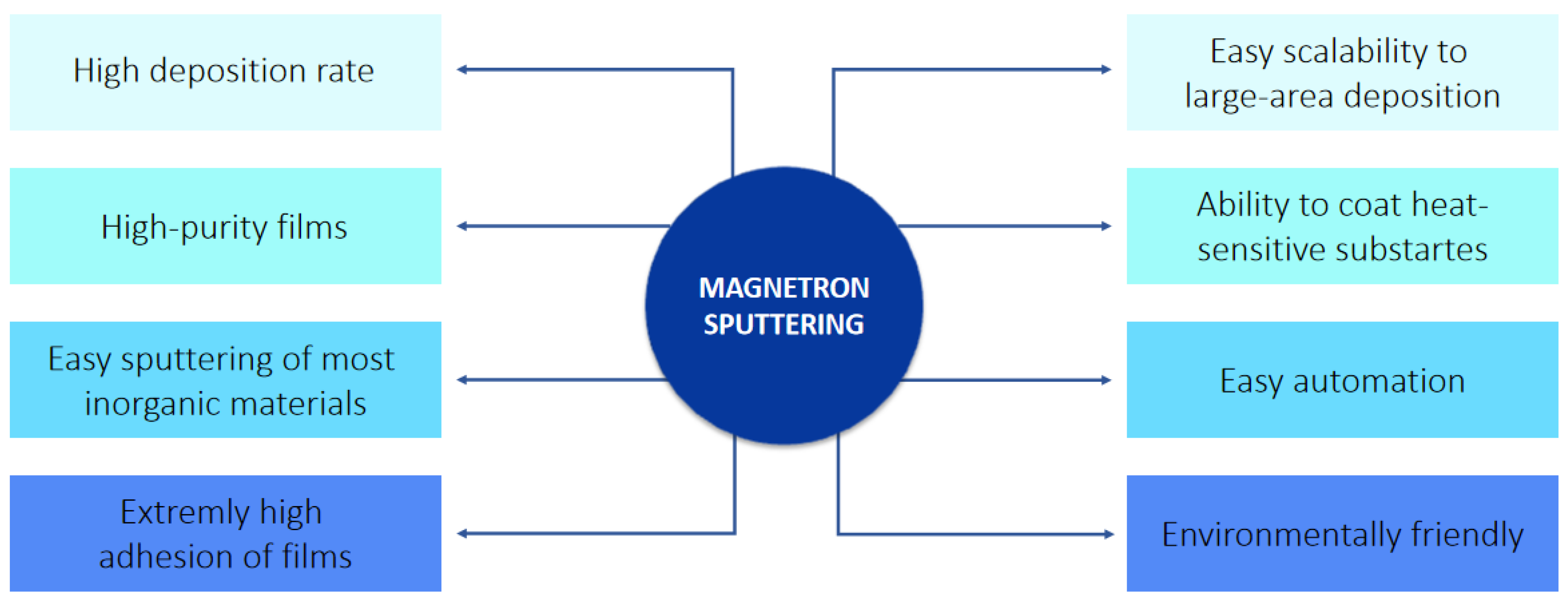
1. Introduction
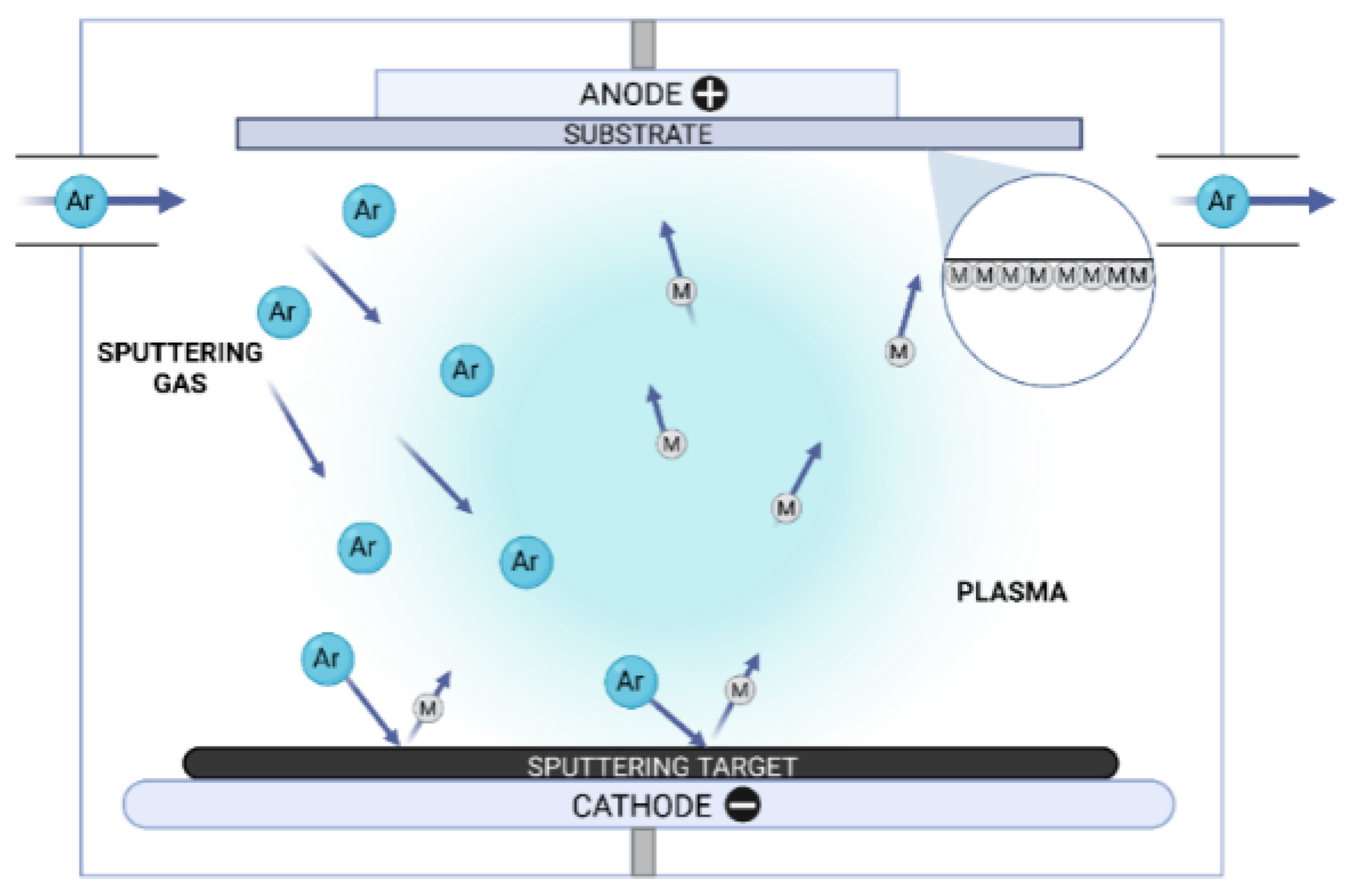
2. Materials and Methods
2.1. Material Characterization
2.2. Photocatalysis Measurement
3. Results
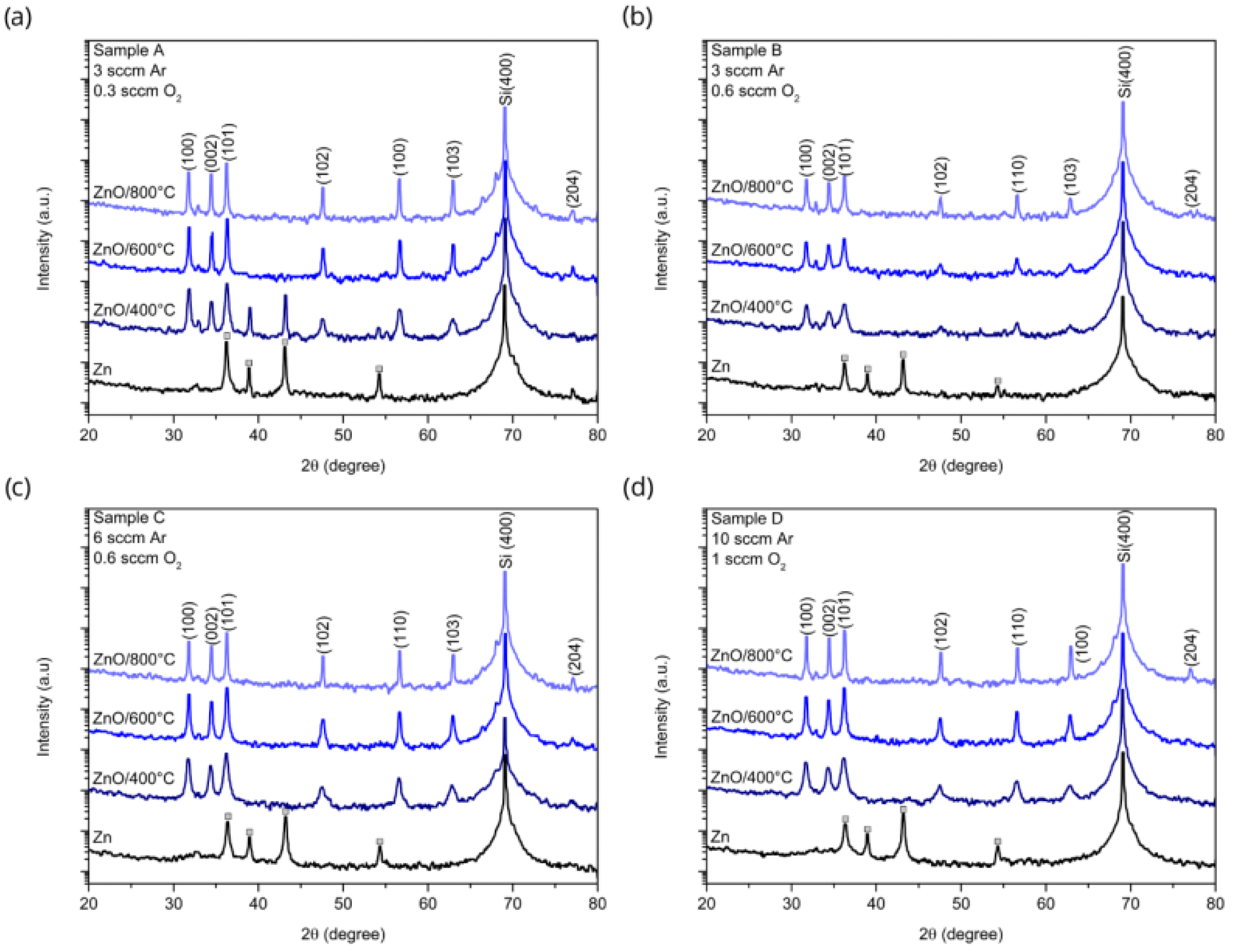
3.1. X-ray Diffraction
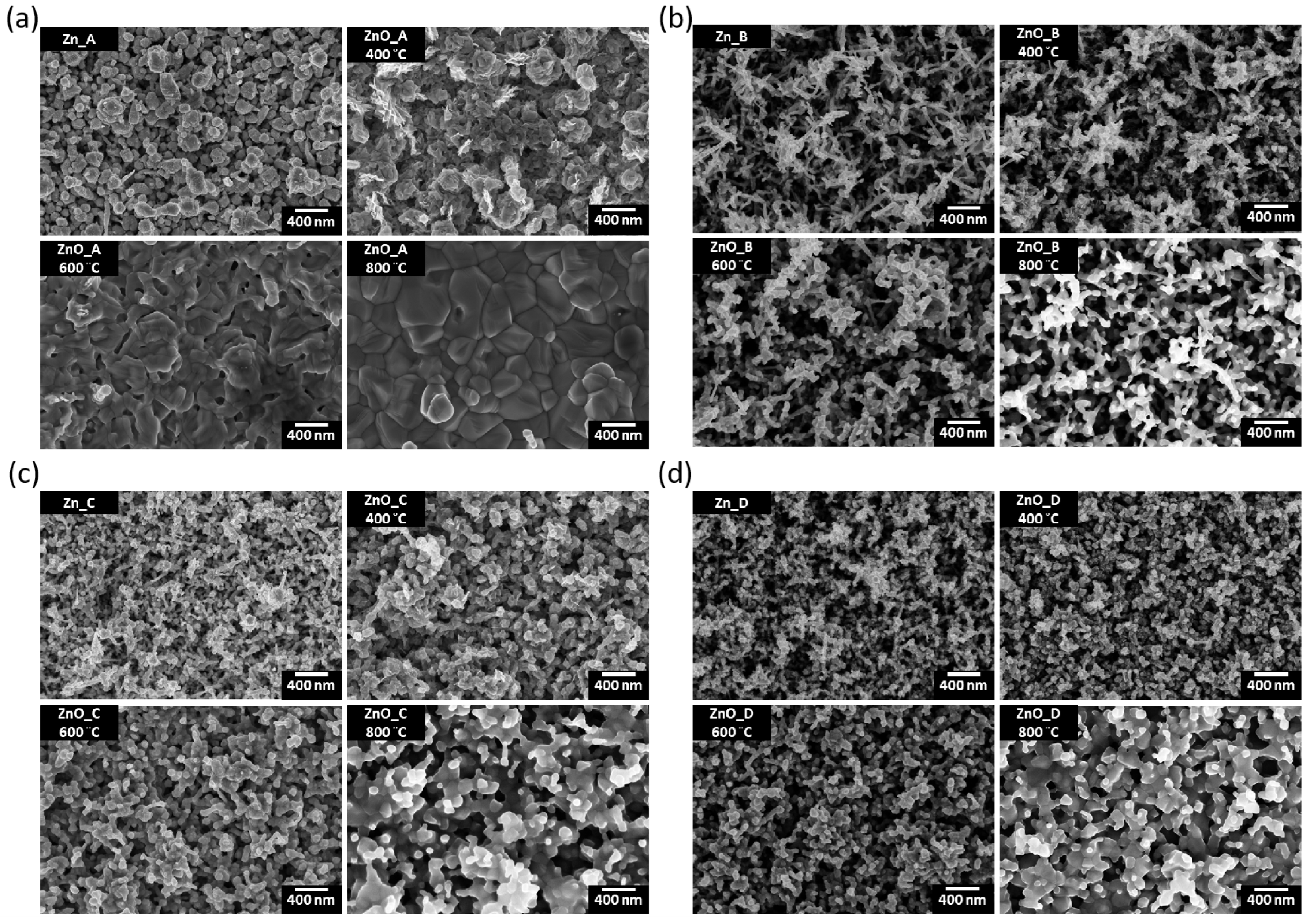
3.2. Scanning Electron Microscopy
3.3. Optical Properties
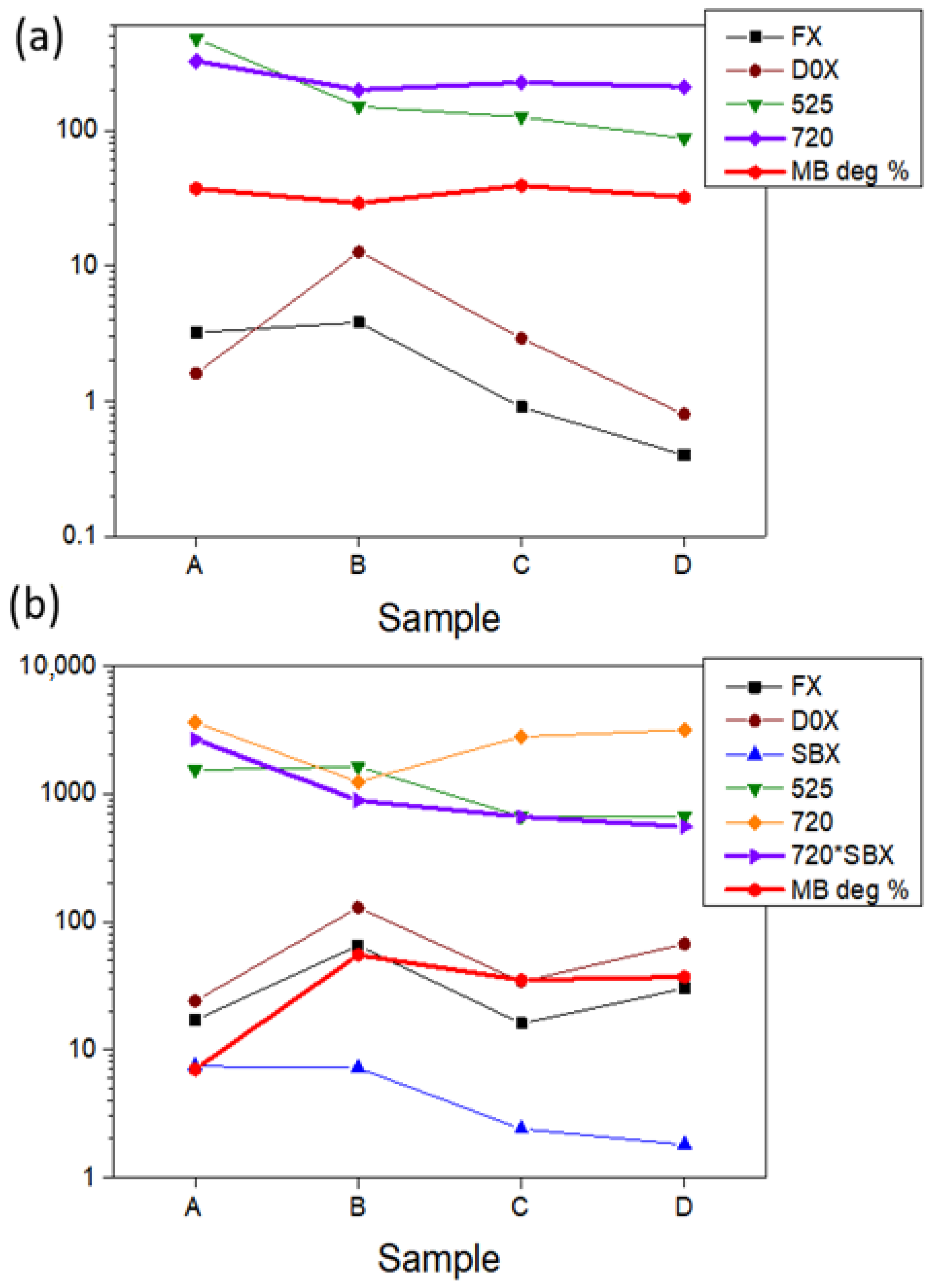
3.4. Photocatalytic Degradation of Methylene Blue by ZnO Thin Films
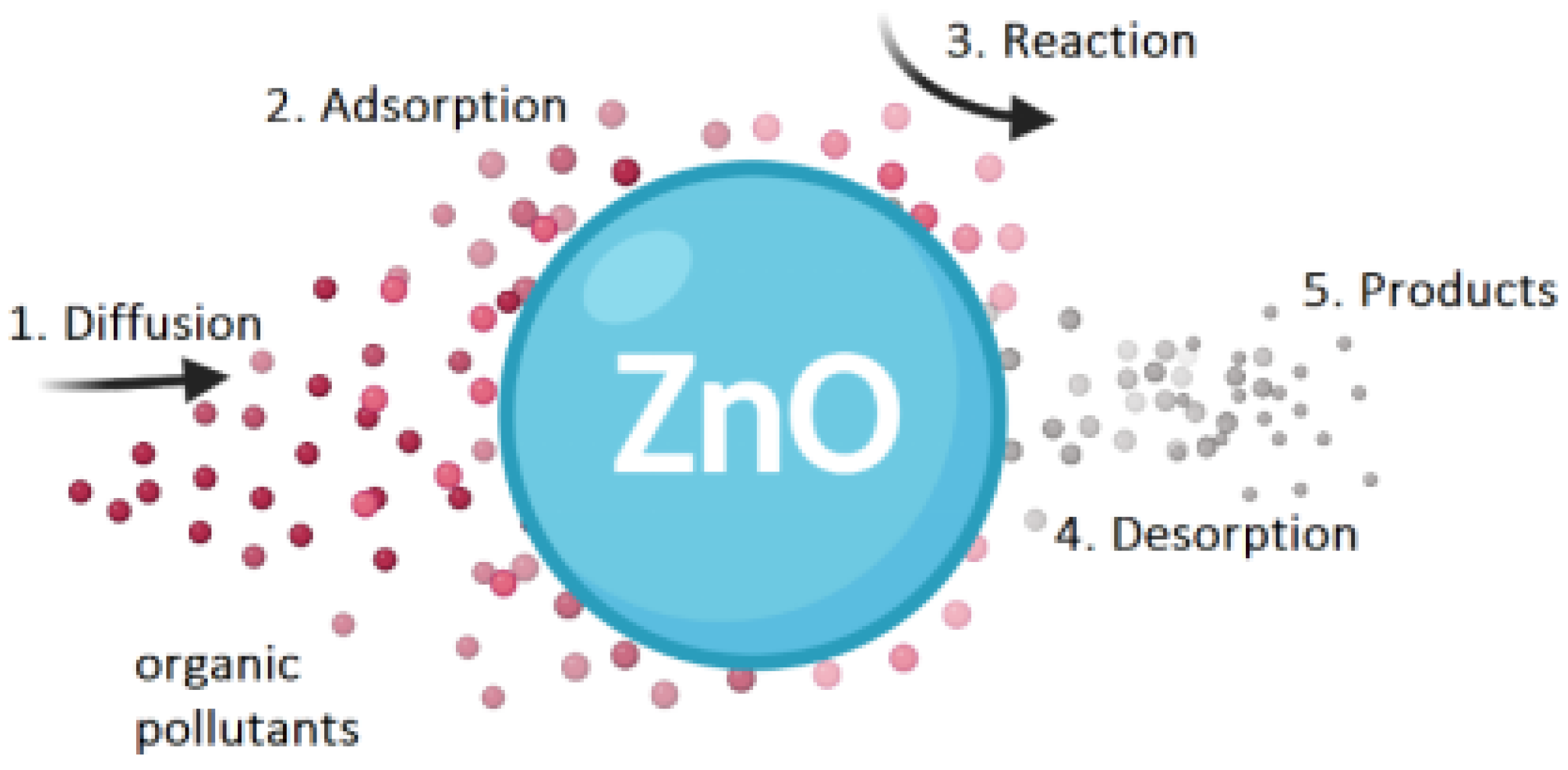
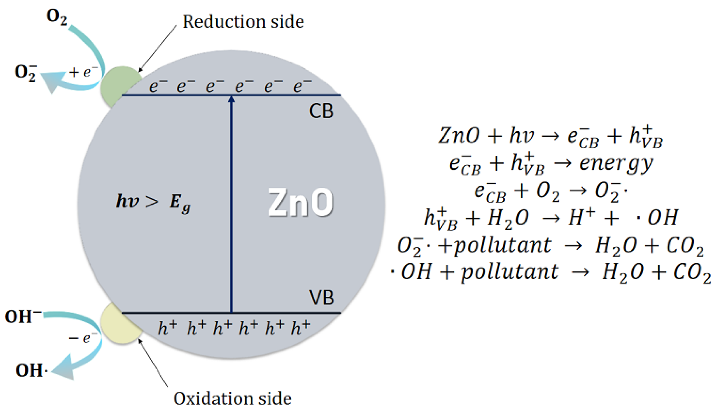
4. Discussion
5. Conclusions
Supplementary Materials
Author Contributions
Funding
Institutional Review Board Statement
Informed Consent Statement
Data Availability Statement
Conflicts of Interest
References
- Kolodziejczak-Radzimska, A.; Jesionowski, T. Zinc Oxide-from Synthesis to Application: A Review. Materials 2014, 7, 2833–2881. [Google Scholar] [CrossRef] [PubMed]
- Muslih, E.Y.; Kim, K.H. Preparation of Zinc Oxide (ZnO) Thin Film as Transparent Conductive Oxide (TCO) from Zinc Complex Compound on Thin Film Solar Cells: A Study of O2 Effect on Annealing Process. IOP Conf. Ser. Mater. Sci. Eng. 2017, 214, 012001. [Google Scholar] [CrossRef]
- Khranovskyy, V.; Yakimova, R. Morphology Engineering of ZnO Nanostructures. Phys. Condens. Matter 2012, 407, 1533–1537. [Google Scholar] [CrossRef]
- Kang, Y.; Yu, F.; Zhang, L.; Wang, W.; Chen, L.; Li, Y. Review of ZnO-Based Nanomaterials in Gas Sensors. Solid State Ionics 2021, 360, 115544. [Google Scholar] [CrossRef]
- Alshammari, F.H.; Nayak, P.K.; Wang, Z.; Alshareef, H.N. Enhanced ZnO Thin-Film Transistor Performance Using Bilayer Gate Dielectrics. ACS Appl. Mater. Interfaces 2016, 8, 22751–22755. [Google Scholar] [CrossRef] [PubMed]
- Fan, J.C.; Sreekanth, K.M.; Xie, Z.; Chang, S.L.; Rao, K.V. P-Type ZnO materials: Theory, growth, properties and devices. Prog. Mater. Sci. 2013, 6, 874–985. [Google Scholar] [CrossRef]
- Kulis-Kapuscinska, A.; Kwoka, M.; Borysiewicz, M.A.; Wojciechowski, T.; Licciardello, N.; Sgarzi, M.; Cuniberti, G. Photocatalytic Degradation of Methylene Blue at Nanostructured ZnO Thin Films. Nanotechnology 2023, 34, 155702. [Google Scholar] [CrossRef]
- Mitra, A.; Thareja, R.K.; Ganesan, V.; Gupta, A.; Sahoo, P.K.; Kulkarni, V.N. Synthesis and Characterization of ZnO Thin Films for UV Laser. Appl. Surf. Sci 2001, 174, 232–239. [Google Scholar] [CrossRef]
- Ameen, S.; Akhtar, M.S.; Song, M.; Shin, H.S. Vertically Aligned ZnO Nanorods on Hot Filament Chemical Vapor Deposition Grown Graphene Oxide Thin Film Substrate: Solar Energy Conversion. ACS Appl. Mater. Interfaces 2012, 4, 4405–4412. [Google Scholar] [CrossRef]
- Johari, S.; Muhammad, N.Y.; Zakaria, M.R. Study of Zinc Oxide Thin Film Characteristics. EPJ Web Conf. 2017, 162, 01057. [Google Scholar] [CrossRef]
- Etcheverry, L.P.; Flores, W.H.; da Silva, D.L.; Moreira, E.C. Annealing Effects on the Structural and Optical Properties of ZnO Nanostructures. Mater. Res. 2018, 21, e20170936. [Google Scholar] [CrossRef]
- Agrawal, S.; Rane, R.; Mukherjee, S. ZnO Thin Film Deposition for TCO Application in Solar Cell. Conf. Pap. Energy 2013, 2013, 718692. [Google Scholar] [CrossRef]
- Kumar, V.; Gohain, M.; Kant, R.; Ntwaeaborwa, O.M.; Hari, P.; Swart, H.C.; Dutta, V. Annealing Induced Oxygen Defects on Green Sonochemically Synthesized ZnO Nanoparticles for Photoelectrochemical Water Splitting. ChemistrySelect 2018, 3, 11914–11921. [Google Scholar] [CrossRef]
- Olejnik-Fehér, N.; Jędrzejewska, M.; Wolska-Pietkiewicz, M.; Lee, D.; De Paëpe, G.; Lewiński, J. On the Fate of Lithium Ions in Sol–Gel Derived Zinc Oxide Nanocrystals. Small 2024, 20, 2309984. [Google Scholar] [CrossRef] [PubMed]
- Mohan, S.; Vellakkat, M.; Aravind, A.; Reka, U. Hydrothermal synthesis and characterization of Zinc Oxide nanoparticles of various shapes under different reaction conditions. Nano Express 2020, 1, 030028. [Google Scholar] [CrossRef]
- Wolska-Pietkiewicz, M.; Tokarska, K.; Grala, A.; Wojewódzka, A.; Chwojnowska, E.; Grzonka, J.; Cywiński, P.J.; Kruczała, K.; Sojka, Z.; Chudy, M.; et al. Safe-by-Design Ligand-Coated ZnO Nanocrystals Engineered by an Organometallic Approach: Unique Physicochemical Properties and Low Toxicity toward Lung Cells. Chem. Eur. J. 2018, 24, 4033–4042. [Google Scholar] [CrossRef]
- Jędrzejewska, M.; Wolska-Pietkiewicz, M.; Drużyński, Z.; Lewiński, J. Organometallic One-Pot Synthesis of ZnO Quantum Dots Coated by Sulfoxides as L-Type Ligands. J. Mater. Chem. C 2023, 11, 15016–15029. [Google Scholar] [CrossRef]
- Tynell, T.; Karppinen, M. Atomic Layer Deposition of ZnO: A Review. Semicond. Sci. Technol. 2014, 29, 043001. [Google Scholar] [CrossRef]
- Triboulet, R.; Perrière, J. Epitaxial Growth of ZnO Films. Prog. Cryst. Growth Charact. Mater. 2003, 47, 65–138. [Google Scholar] [CrossRef]
- Yudasari, N.; Kennedy, D.S.; Suliyanti, M.M. Pulse Laser Deposition (PLD) Technique for ZnO Photocatalyst Fabrication. J. Phys. Conf. Ser. 2019, 1191, 012009. [Google Scholar] [CrossRef]
- Borysiewicz, M.A.; Dynowska, E.; Kolkovsky, V.; Dyczewski, J.; Wielgus, M.; Kamińska, E.; Piotrowska, A. From Porous to Dense Thin ZnO Films through Reactive DC Sputter Deposition onto Si (100) Substrates. Phys. Status Solidi Appl. Mater. Sci. 2012, 209, 2463–2469. [Google Scholar] [CrossRef]
- Tudose, I.V.; Comanescu, F.; Pascariu, P.; Bucur, S.; Rusen, L.; Iacomi, F.; Koudoumas, E.; Suchea, M.P. Chemical and Physical Methods for Multifunctional Nanostructured Interface Fabrication. In Functional Nanostructured Interfaces for Environmental and Biomedical Applications; Elsevier: Amsterdam, The Netherlands, 2019; pp. 15–26. [Google Scholar]
- Kwoka, M.; Lyson-Sypien, B.; Kulis, A.; Maslyk, M.; Borysiewicz, M.A.; Kaminska, E.; Szuber, J. Surface Properties of Nanostructured, Porous ZnO Thin Films Prepared by Direct Current Reactive Magnetron Sputtering. Materials 2018, 11, 131. [Google Scholar] [CrossRef] [PubMed]
- Wan, Q.; Wang, T.H.; Zhao, J.C. Enhanced Photocatalytic Activity of ZnO Nanotetrapods. Appl. Phys. Lett. 2005, 87, 083105. [Google Scholar] [CrossRef]
- Tran, T.H.; Tran, T.N.A.; Bach, T.C.; Sai, C.D.; Pham, N.H.; Tran, V.T.; Nguyen, T.B.; Nguyen, Q.H.; Pham, V.T.; Doan, Q.K.; et al. Effect of annealing on the properties of transparent conducting Ag doped ZnO thin films prepared by r.f. magnetron sputtering method. Micro Nanostruct. 2022, 166, 207219. [Google Scholar] [CrossRef]
- Kim, W.Y.; Kim, S.W.; Yoo, D.H.; Kim, E.J.; Hahn, S.H. Annealing Effect of ZnO Seed Layer on Enhancing Photocatalytic Activity of ZnO/TiO2 Nanostructure. Int. J. Photoenergy 2013, 2013, 130541. [Google Scholar] [CrossRef]
- Suguna, A.; Prabhu, S.; Selvaraj, M.; Geerthana, M.; Silambarasan, A.; Navaneethan, M.; Ramesh, R.; Sridevi, C. Annealing Effect on Photocatalytic Activity of ZnO Nanostructures for Organic Dye Degradation. J. Mater. Sci. Mater. Electron. 2022, 33, 8868–8879. [Google Scholar] [CrossRef]
- Janotti, A.; Van De Walle, C.G. Native point defects in ZnO. Phys. Rev. B 2007, 76, 165202. [Google Scholar] [CrossRef]
- Ong, C.B.; Ng, L.Y.; Mohammad, A.W. A Review of ZnO Nanoparticles as Solar Photocatalysts: Synthesis, Mechanisms and Applications. Renew. Sustain. Energy Rev. 2018, 81, 536–551. [Google Scholar] [CrossRef]
- Ancona, A.; Dumontel, B.; Garino, N.; Demarco, B.; Chatzitheodoridou, D.; Fazzini, W.; Engelke, H.; Cauda, V. Lipid-Coated Zinc Oxide Nanoparticles as Innovative ROS-Generators for Photodynamic Therapy in Cancer Cells. Nanomaterials 2018, 8, 143. [Google Scholar] [CrossRef]
- Saravanan, R.; Gupta, V.K.; Narayanan, V.; Stephen, A. Comparative Study on Photocatalytic Activity of ZnO Prepared by Different Methods. J. Mol. Liq. 2013, 181, 133–141. [Google Scholar] [CrossRef]
- Mohamed, K.M.; Benitto, J.J.; Vijaya, J.J.; Bououdina, M. Recent Advances in ZnO-Based Nanostructures for the Photocatalytic Degradation of Hazardous, Non-Biodegradable Medicines. Crystals 2023, 13, 329. [Google Scholar] [CrossRef]
- Saha, D.; Desipio, M.M.; Hoinkis, T.J.; Smeltz, E.J.; Thorpe, R.; Hensley, D.K.; Fischer-Drowos, S.G.; Chen, J. Influence of hydrogen peroxide in enhancing photocatalytic activity of carbon nitride under visible light: An insight into reaction intermediates. J. Environm. Chem. Eng. 2018, 6, 4927–4936. [Google Scholar] [CrossRef]
- Pędziwiatr, P.; Mikołajczyk, F.; Zawadzki, D.; Mikołajczyk, K.; Bedka, A. Decomposition of hydrogen peroxide—Kinetics and review of chosen catalysts. Acta Innov. 2018, 26, 45–52. [Google Scholar] [CrossRef]
- Borysiewicz, M.A.; Wzorek, M.; Wojciechowski, T.; Wojtowicz, T.; Kamińska, E.; Piotrowska, A. Photoluminescence of nanocoral ZnO films. J. Lumin. 2014, 147, 367–371. [Google Scholar] [CrossRef]
- Masłyk, M.; Borysiewicz, M.A.; Wzorek, M.; Wojciechowski, T.; Kwoka, M.; Kamińska, E. Influence of absolute argon and oxygen flow values at a constant ratio on the growth of Zn/ZnO nanostructures obtained by DC reactive magnetron sputtering. Appl. Surf. Sci. 2016, 389, 287–293. [Google Scholar] [CrossRef]
- Nizar, B.M.; Lajnef, M.; Chaste, J.; Chtourou, R.; Herth, E. Highly C-Oriented (002) Plane ZnO Nanowires Synthesis. RSC Adv. 2023, 13, 15077–15085. [Google Scholar] [CrossRef]
- Wei, X.Q.; Zhang, Z.G.; Liu, M.; Chen, C.S.; Sun, G.; Xue, C.S.; Zhuang, H.Z.; Man, B.Y. Annealing Effect on the Microstructure and Photoluminescence of ZnO Thin Films. Mater. Chem. Phys. 2007, 101, 285–290. [Google Scholar] [CrossRef]
- Zeng, H.; Duan, G.; Li, Y.; Yang, S.; Xu, X.; Cai, W. Blue Luminescence of ZnO Nanoparticles Based on Non-Equilibrium Processes: Defect Origins and Emission Controls. Adv. Funct. Mater. 2010, 20, 561–572. [Google Scholar] [CrossRef]
- Shen, H.; Shi, X.; Wang, Z.; Hou, Z.; Xu, C.; Duan, L.; Zhao, X.; Wu, H. Defects Control and Origins of Blue and Green Emissions in Sol-Gel ZnO Thin Films. Vacuum 2022, 202, 111201. [Google Scholar] [CrossRef]
- Hsieh, P.T.; Chin, H.S.; Chang, P.K.; Wang, C.M.; Chen, Y.C.; Houng, M.P. Effects of the Annealing Environment on Green Luminescence of ZnO Thin Films. Phys. B Condens. Matter 2010, 405, 2526–2529. [Google Scholar] [CrossRef]
- Janotti, A.; Van de Walle, C.G. Fundamentals of ZnO as a semiconcutor. Rep. Prog. Phys. 2009, 72, 126501. [Google Scholar] [CrossRef]
- Leiter, F.H.; Alves, H.R.; Hofstaetter, A.; Hofmann, D.M.; Meyer, B.K. The Oxygen Vacancy as the Origin of a Green Emission in Undoped ZnO. Phys. Status Solidi 2001, 226, R4–R5. [Google Scholar] [CrossRef]
- Lv, J.; Li, C. Evidences of VO, VZn, and Oi defects as the green luminescence origins in ZnO. Appl. Phys. Lett. 2013, 103, 232114. [Google Scholar] [CrossRef]
- Teklemichael, S.T.; McCluskey, M.D. Acceptor and surface states of ZnO nanocrystals: A unified model. Nanotechnology 2011, 22, 475703. [Google Scholar] [CrossRef] [PubMed]
- Galdámez-Martinez, A.; Santana, G.; Güell, F.; Martínez-Alanis, P.R.; Dutt, A. Photoluminescence of ZnO Nanowires: A Review. Nanomaterials 2020, 10, 857. [Google Scholar] [CrossRef] [PubMed]
- Kumar, V.; Swart, H.C.; Ntwaeaborwa, O.M.; Kroon, R.E.; Terblans, J.J.; Shaat, S.K.K.; Yousif, A.; Duvenhage, M.M. Origin of the red emission in zinc oxide nanophosphors. Mater. Lett. 2013, 101, 57–60. [Google Scholar] [CrossRef]
- Willander, M.; Nur, O.; Sadaf, J.R.; Qadir, M.I.; Zaman, S.; Zainelabdin, A.; Bano, N.; Hussain, I. Luminescence from Zinc Oxide Nanostructures and Polymers and Their Hybrid Devices. Materials 2010, 3, 2643–2667. [Google Scholar] [CrossRef]
- Neena, D.; Kondamareddy, K.K.; Bin, H.; Lu, D.; Kumar, P.; Dwivedi, R.K.; Pelenovich, V.O.; Zhao, X.Z.; Gao, W.; Fu, D. Enhanced visible light photodegradation activity of RhB/MB from aqueous solution using nanosized novel Fe-Cd co-modifed ZnO. Sci. Rep. 2018, 8, 10691. [Google Scholar]
- Ferreira, N.S.; Sasaki, J.M.; Silva, R.S., Jr.; Attah-Baah, J.M.; Macêdo, M.A. Visible-Light-Responsive Photocatalytic Activity Significantly Enhanced by Active [VZn+VO+] Defects in Self-Assembled ZnO Nanoparticles. Inorg. Chem. 2021, 60, 4475–4496. [Google Scholar] [CrossRef]
- Jang, Y.J.; Simer, C.; Ohm, T. Comparison of zinc oxide nanoparticles and its nano-crystalline particles on the photocatalytic degradation of methylene blue. Mater. Res. Bull. 2006, 41, 67–77. [Google Scholar] [CrossRef]
- Song, S.; Wu, K.; Wu, H.; Guo, J.; Zhang, L. Multi-shelled ZnO decorated with nitrogen and phosphorus co-doped carbon quantum dots: Synthesis and enhanced photodegradation activity of methylene blue in aqueous solutions. RSC Adv. 2019, 9, 7362–7374. [Google Scholar] [CrossRef] [PubMed]


| Catalyst | Light Source | Mass of ZnO (mg) | Volume of Solution (mL) | MB Concentration () | Irradiation Time (min) | MB Degradation (%) | Reference |
|---|---|---|---|---|---|---|---|
| Sol-gel, sintered 600 °C | Visible | 100 | 100 | 20 | 120 | 25 | [49] |
| Calcinated 700 °C | 430 nm, 100 W | 10 | 50 | 50 | 120 | 30.67 | [50] |
| Flame spray pyrolysis | 365 nm, 20 W | 1500 | 650 | 15 | 60 | 99 | [51] |
| Multi-shelled decorated | Xenon lamp, 300 W | 20 | 200 | 10 | 30 | 90 | [52] |
| Sample B-800 °C | UVA lamp, 6 W | 0.4 | 50 | 50 | 120 | 40 | This work |
Disclaimer/Publisher’s Note: The statements, opinions and data contained in all publications are solely those of the individual author(s) and contributor(s) and not of MDPI and/or the editor(s). MDPI and/or the editor(s) disclaim responsibility for any injury to people or property resulting from any ideas, methods, instructions or products referred to in the content. |
© 2024 by the authors. Licensee MDPI, Basel, Switzerland. This article is an open access article distributed under the terms and conditions of the Creative Commons Attribution (CC BY) license (https://creativecommons.org/licenses/by/4.0/).
Share and Cite
Ćwik, K.; Zawadzki, J.; Zybała, R.; Ożga, M.; Witkowski, B.; Wojnar, P.; Wolska-Pietkiewicz, M.; Jędrzejewska, M.; Lewiński, J.; Borysiewicz, M.A. Magnetron Sputtering as a Solvent-Free Method for Fabrication of Nanoporous ZnO Thin Films for Highly Efficient Photocatalytic Organic Pollution Degradation. Compounds 2024, 4, 534-547. https://doi.org/10.3390/compounds4030032
Ćwik K, Zawadzki J, Zybała R, Ożga M, Witkowski B, Wojnar P, Wolska-Pietkiewicz M, Jędrzejewska M, Lewiński J, Borysiewicz MA. Magnetron Sputtering as a Solvent-Free Method for Fabrication of Nanoporous ZnO Thin Films for Highly Efficient Photocatalytic Organic Pollution Degradation. Compounds. 2024; 4(3):534-547. https://doi.org/10.3390/compounds4030032
Chicago/Turabian StyleĆwik, Kamila, Jakub Zawadzki, Rafał Zybała, Monika Ożga, Bartłomiej Witkowski, Piotr Wojnar, Małgorzata Wolska-Pietkiewicz, Maria Jędrzejewska, Janusz Lewiński, and Michał A. Borysiewicz. 2024. "Magnetron Sputtering as a Solvent-Free Method for Fabrication of Nanoporous ZnO Thin Films for Highly Efficient Photocatalytic Organic Pollution Degradation" Compounds 4, no. 3: 534-547. https://doi.org/10.3390/compounds4030032
APA StyleĆwik, K., Zawadzki, J., Zybała, R., Ożga, M., Witkowski, B., Wojnar, P., Wolska-Pietkiewicz, M., Jędrzejewska, M., Lewiński, J., & Borysiewicz, M. A. (2024). Magnetron Sputtering as a Solvent-Free Method for Fabrication of Nanoporous ZnO Thin Films for Highly Efficient Photocatalytic Organic Pollution Degradation. Compounds, 4(3), 534-547. https://doi.org/10.3390/compounds4030032