Review

Surface Engineering for Enhanced Triboelectric Nanogenerator

1
Jiangsu Key Laboratory for Carbon-Based Functional Materials and Devices, Institute of Functional Nano and Soft Materials (FUNSOM), Soochow University, Suzhou 215123, China
2
Department of Chemistry, Faculty of Science, New Valley University, El-Kharja 72511, Egypt
*
Authors to whom correspondence should be addressed.
These authors contributed equally to this work.
Nanoenergy Adv. 2021, 1(1), 58-80; https://doi.org/10.3390/nanoenergyadv1010004
Submission received: 16 July 2021 / Revised: 13 September 2021 / Accepted: 14 September 2021 / Published: 18 September 2021
(This article belongs to the Special Issue Recent Advances in Nanogenerators)

Abstract

:
Triboelectric nanogenerator (TENG) is the new technique that can convert low-frequency mechanical energy into effective electricity. As an energy collector, the pursuit of high output characteristics is understandable. Although high charge density has been achieved by working in high vacuum or charge pumping techniques, it remains challenging to obtain the high output performance directly in the atmosphere. Herein, surface-engineering of the triboelectric layer for enhancing output performance has been reviewed carefully. By constructing surface morphology or developing surface modification, high performance of TENGs is finally presented in the review.

1. Introduction

Researchers have been devoting efforts towards the development of clean and renewable energy, with the increasing energy issue. However, it is still a major challenge facing humanity [1,2]. One of the most widespread energy sources is mechanical energy. Researchers have designed devices for mechanical energy, including electromagnetic, thermoelectric, piezoelectric, and triboelectric nanogenerators [3,4,5,6,7,8,9,10,11,12,13,14,15,16,17,18]. Triboelectric nanogenerators (TENGs) can be applied to harvest all types of mechanical energies, such as human movement, rotating tires, vibration, wind, flowing water, and other sources that can produce triboelectrification [19]. Since its first invention in 2012, TENG is a type of energy harvesting device that transforms biomechanical energy into effective electricity. It was demonstrated in Wang’s group via the coupling effects of triboelectrification and electrostatic induction [11,20]. When the surface of two triboelectric materials come in contact with each other, opposite charges will be created on the surface. Once the two surfaces are separated by external force, a potential difference is created, thus generating voltage. Then, the charge flows due to the electrostatic induction to maintain electrostatic equilibrium.
Meanwhile, studies reveal that TENG has many advantages, including low fabrication cost, light weight, and high energy efficiency. Besides, the materials selection and device structure of the fabrication of TENG is wide [21,22]. Therefore, many researchers have been developing various types of TENG [23,24,25,26,27,28,29,30]. The contact area between two triboelectric layers plays a major effect on TENG’s properties [31,32,33,34,35,36,37,38,39,40,41,42,43,44,45,46,47]. There have been previous works focused on materials selection [48,49,50,51,52,53,54], surface modification [41,55,56,57,58,59,60,61,62,63], and control of surface topography [64,65,66] to investigate the triboelectrification mechanism on the performance of triboelectric nanogenerators. While materials selection is dependent on choosing the triboelectric contact pairs, far apart in triboelectric series depends on which materials have opposite polarity. Another way to study the triboelectrification mechanism is the control of surface topography to improve the output performance of the optimized device. However, the method of surface modification is more effective for increasing the efficiency of TENGs that are modified through chemical and physical methods, with material selection and structural design.
Within the review, various engineering strategies that improve output performance of TENG will be introduced accordingly, as shown in Figure 1. The first and second parts are a brief introduction and performance of TENG. The third part includes surface engineering methods that play a big role in the TENGs output, which are divided into two parts: surface morphology and surface modification. The strategies for surface morphology and surface modification to enhance the TENG output will be introduced. Finally, perspective and outline for future application in designing high performance of TENGs will be introduced in part four.

2. Triboelectric Nanogenerator

2.1. Origin of Triboelectric Nanogenerator

The scientific term for TE is contact electrification (CE) phenomenon, in which it results from physical contact between two materials without rubbing against each other and the transfer of electrons from one material to another. With this process of charge transfer during contact and separation, the surface charge density, polarization, and strength of the charges are strongly dependent on the materials, which helps in understanding the TE mechanism. Since the invention of TENG, Wang et al. have devoted many efforts in the analysis of the origin of triboelectric nanogenerator [18]. Research indicates that electron transfer is the dominant mechanism for CE between solid-solid pairs, and the electron transfer model can be extended to other pairs.

2.2. Choice of Materials

All known materials such as wood, polymers, metals, and silk show the effect of triboelectrification. All materials can be applied for TENG fabrication. The material selection for TENG is large because the original reason is gaining/losing electrons that are dependent on the polarity difference of material pairs. John Carl Wilcke published a paper in 1757 on static charges about the first triboelectric series [70]. The material at the bottom of the chain, when touching a material close to the upper of the chain, will get a negative charge. As such, materials that accept electrons tend to obtain a negative charge, while those that lose electrons become positively charged [71]. When choosing triboelectric material, it is important to consider the surface charge matching of two tribo-layers. This means that we need to choose two materials with quite different triboelectric series, and if we choose the materials with similar triboelectric series, the output performance will be influenced to a large extent.

3. Surface Engineering Methods

The surface charge density of triboelectric materials is the key point that leads to the high output performance of TENG [72]. The surface charge density is determined in the triboelectric layer via the electron-donation or accepting ability. This section reviews many functionalization techniques for improving the TENGs output performance.

3.1. Surface Morphology

Triboelectric material morphology engineering refers to the modification of the material surface. To increase the contact area between friction layers in micro/nano surface patterns, morphological engineering is used to improve the output performances in triboelectric energy harvesters, therefore increase the effective charge density. The physical surface modification is done through the introduction of the micro/nano surface on the electro-frictional layers by using different mechanical methods, such as soft lithography [73,74,75], photolithography [76,77,78], and ultrafast laser patterning [79,80,81].

3.1.1. Soft Lithography

Researchers have developed micro/nano structures for growing the roughness, which has been introduced to improve the TENG output.
Wang et al. [67] proposed the rational design of an arch-shaped structure based on the contact electrification between a polymer and a metal film. In Figure 2a, the structural process of the arch-shaped triboelectric nanogenerator relies on the electrical contact between patterned polydimethylsiloxane (PDMS) and patterned Al foil on the top and the bottom plate, respectively. The patterned surfaces of PDMS film and Al foil are fabricated to enhance the triboelectric charging, and they are characterized using scanning electron microscopy (SEM). Both arrays are uniform and regular across a very large area in Figure 2b. The working mechanism of the TENG was studied by finite element simulation. According to the TENG output voltage and current at a range of frequency (2–10 Hz) in Figure 2c, noted that with the triggering frequency of 6 Hz and controlled amplitude, the accumulation of the triboelectric charges increases and reaches equilibrium in a certain time after multiple cycles. Then, the output will gradually go up in the first stage, where generated 230 V, 15.5 μAcm−2, and energy volume density reached 128 mWcm−3, while the energy efficiency is produced 10−39%.
To further improve the output performance, Zhang et al. [82] proposed dual scale structures on TENG output. As schematically presented in Figure 2d, a sandwich-shaped triboelectric nanogenerator is composed of a 20 μm thick aluminum film with 450 μm thick PDMS film fixed with elastic tape between two surface micro/nanostructured to form a sandwich-shaped structure. On the top, the PDMS film fabricated 125 μm thick PET/ITO thin film. The well-designed micro/nano dual-scale structure (i.e., pyramids and V-shape grooves) is fabricated by using photolithography and KOH wet etching at the top of the PDMS surface. As shown in Figure 2e, the output peak voltage, current density, and power density achieved 465 V, 13.4 μAcm−2, and 53.4 mWcm−3, respectively. Noted that the pure micro-structures or nanostructures can decrease the roughness faster than the dual-scale structure, hence strengthening the performance of TENG. Moreover, the voltage and the current micro/nano dual-scale with pyramid, compared to that of flat PDMS film, enhanced by 100% and 157%. Likewise, Kim et al. [61] suggested a large area nano patterning technique, where block copolymer (BCP) by lithography technique was introduced on a flexible gold substrate. As illustrated in Figure 2f, Au (100 nm) is deposited on cleaned Kapton film by thermal evaporation of the metal layer. After lifting the BCP template, an Au nanodot was formed on the surface of the Au. As shown in Figure 2g, the generated short-circuit currents and open-circuit voltages from the flat Au are 22 µA and 55 V, respectively. Comparatively, the generated short-circuit currents and open-circuit voltages from nanopatterned Au are 82 µA and 225 V, respectively. The Nanopatterned Au contact surface has a larger effective contact area than the flat Au surface; more electric charge is induced by contact-electrification, dramatically enhancing the output performance with an output power density of 93.2 Wm−2. After BCP nanopatterning, TENG output currents improved up to 16 times due to the increased contact area.
A new design can develop the output of the nanogenerator efficiency by increasing the triboelectric effect and the capacitance change, where Fen ta al [65] proposed the first thin film micro patterned PDMS with different features such as patterned lines, cubes, and pyramids as triboelectric contact layers to improve the output of TENG. As illustrated in Figure 3a–c, during the fabrication process, Si wafer molds were fabricated by the traditional photolithography method to make patterned PDMS as a friction layer with various features including lines, cubes, and pyramids. The PDMS film was fixed on the surface of a clean ITO-coated polyester (PET) substrate and wrapped with the other ITO-coated PET film to form a structured sandwich device. Comparison of the open-circuit voltage and current is as illustrated in Figure 3d. The results reveal that the maximum output voltage is up to 18 V and current is 0.7 μA for pyramid-surface structure, which is four times compared to TENG using flat films. Similar to this work, various physical surface modification has been used in micro/nano structures [27,83,84,85,86]. For example, Sun et al. made micro-nano structures on the PDMS by leaves mold with rich surface textures [85]. Besides, the micro-structured PDMS film can also be made through low surface energy sandpaper template without the use of surfactant coating or high vacuum [86].

3.1.2. Ultrafast Laser Patterning

Ultrafast laser irradiation is used to control in the PDMS surface morphology by using it for micro/nano hierarchical structures fabrication. Femtosecond laser offers a flexible method in open air for mask-free fabrication of micro/nano structures, due to its short irradiation period and superior intensity [87,88,89].
The femtosecond laser was first used in producing micro/nano structures on polydimethylsiloxane (PDMS) film by Kim et al. [90]. After femtosecond laser direct writing, the effective contact area between the friction layer is improved, thus improving the output performance of TENG. As illustrated in Figure 4a, a schematic illustration of the ultrafast laser irradiation method was used on the PDMS surface patterning. The TENG is composed of PDMS and aluminum. Aluminum is used as the top electrode. The counter-electrode in the PDMS is another aluminum, which is connected from the back side of PDMS. In this method, the LI-TENG using a laser power of 29 mW in the PDMS patterned to produce a maximum voltage and current with a power density of 42.5 V and 10.1 μA, 107.3 μWcm−2, respectively, as shown in Figure 4b. The largest enhancement in output power, based on the micro structured PDMS, was raised more than two times from the controlled TENG (bare PDMS). Such a fast, direct-writing approach has the potential to make controlled hierarchical micro/nanostructures on different materials.
Except for flexible PDMS, writing directly on Cu can also enhance the output performance. Huang et al. [91] proposed micro/nano structures optimized for TENGs using the method of writing directly on both triboelectric layers by a femtosecond laser such as Cu and PDMS. As shown in Figure 4c, to make micro-bowl structures single-pulse irradiation in different sizes was used on PDMS surfaces. The micro/nano dual-scale structures on Cu film surfaces are fabricated using laser scanning technology in cones and stripes, as illustrated in Figure 4d. TENGs are fabricated with the contact area and contact distance of 8 × 8 mm2 and 1 cm, respectively. The fabricated TENG is tested under the frequency of 1.5 Hz and contact forces at 2 N. Figure 4e shows the voltage (VOC), charge (QSC), and current (ISC) of the TENGs. The results showed that all TENG output performances with different micro/nano structures significantly increased, compared with TENG (0Cu-0PDMS) without micro/nano structures that follows the sequence: TENG2Cu–2P > TENG1Cu–2P > TENG2Cu–1P > TENG1Cu–1P > TENG0Cu–0P. The TENG2Cu–2P with cones and bowls micro/nano structures on Cu surface in a larger size on PDMS surface has the optimal performances. The TENG2Cu–2P produced a voltage of 22.04 V, which is improved by 4.13 times of the TENG0Cu–0P, indicating the effective surface morphology engineering.
Except for lithography and laser patterning, there are other physical methods that can fabricate microstructures such as reactive ion etching (RIE) and electrospinning. These methods can also improve the output performance. For example, Zhai et al. [92] enhanced the output performance of freestanding mode TENG by treating the triboelectric PTFE film with RIE, but these methods have the drawback that it is difficult to control the shape of the microstructure. So, it is just regarded as a pre-processing step in most research, but it is undeniable that this can indeed improve the output performance of TENG.

3.2. Surface Modification

3.2.1. Chemical Functional Groups

In the literature, researchers have used various techniques of surface functionalization to improve the TENG output. To study the effect of chemical functional groups on the output performance of TENG, several studies have focused on introducing functional groups that improve the triboelectric charge transfer, such as self-assembled monolayer (SAM) techniques. As shown in Figure 5a, Wang et al. [62] analyzed chemical surface functionalization by using scanning Kelvin probe microscopy (SKPM), which demonstrated across the major group of SAMs by varying the surface potential. There were four head functional groups (OH, COOCH3, NH2, and Cl) through thiol- based SAM treatment for 12 h, forming in solutions containing different types of thiols on the Au surface. As a result, shown in Figure 5b, the largest enhancement in electrical output with amine groups was raised more than four times from the contact electrification with FEP. The increased output power, after functionalization with these groups, follows the sequence order: hydroxyl, ester, and amine from 4-amino thiophenol. The chlorinate functional group lead to a decrease of the TENG’s output compared to the pristine material, due to the lower charge density. Besides, as shown in Figure 5c, SAM surface functionalization of SiO2 acts as the triboelectric layer in TENGs. After being deposited by plasma chemical vapor deposition on a glass substrate, one kind of silane molecule(3-aminopropyl) triethoxysilane (APTES) was used to form a SAM via three Si-O bonds for each molecule. After functionalization in 10% APTES concentration, transferred charge density, the open-circuit voltage, and short-circuit current density reached 51 µCm−2, 240 V, and 1.75 mAm−2, respectively, as illustrated in Figure 5d. Compared with that produced by 1% APTES concentration, SiO2 has higher chemical potential and can generate more positive charge during contact. So, a higher concentration from APTES is better to improve the output performance.
After demonstrating the effect of SMA on output performance, researchers began to perform more tests on the effect of different kinds of SAMs. Song et al. [66] modified the triboelectric surfaces molecularly engineered by different self-assembled monolayers, such as 3-aminopropyltriethoxysilane (APTES), 3-glycidoxypropyl- triethoxysilane (GPTES), 1H,1H,2H,2H-perfluorooctyltrichloro-silane (FOTS), and trichloro (3,3,3-trifluoropropyl) silane (TFPS) to study the effect of SAMs on the triboelectric properties, shown in Figure 5e. After contact with aluminum foil at the same frequency and force, open circuit voltage (VOC) and the short circuit current (ISC) of APTES, GPTES, FOTS, and TFPS were measured, which is illustrated in Figure 5f. For the PDMS surface treated with either TFPS or FOTS, the open circuit voltage is (105 V) and open circuit current is (27.2 μA) based on FOTS-METS device are six and four times higher than that of pure PDMS/Al device. However, after comparing the VOC and ISC of FOTS, both highest values of the TFPS-METS device decreased. This is due to the fluorine atoms that have lower surface density. On the other hand, when the PDMS surface was treated with either APTES and GPTES, VOC and ISC have negative values for APTES and GPTES confirmed positive charge on the surface of PDMS with these SAMs. As a result, the output performance of TENG was dependent upon end-functional groups of SAMs that formed on PDMS substrate.
Likewise, Byun et al. [93] also proposed the triboelectric series modified by SAM- materials through controlling the surface dipoles and surface electronic states with different electron-donating and withdrawing functional groups. As shown in Figure 6a, the substrate was engineered with four SAM functional groups such as -NH2, -SH, -CH3, and -CF3. After chemical surface modification, the surface potential increased when using the highly electronegative atom F, and decreased when using -NH2, -SH, and -CH3 groups because they electron donated to the metal. KPFM mode in atomic force microscopy (AFM) measurements were used to verify the triboelectricity affected by the surface modification [94]. The charge numbers on the various SAM-modified substrates were explained by contact potential difference (CPD). The surface potential of the substrate, Φsubstrate, is defined as
Φ s u b s t r a t e = Φ p r o b e e · V C P D
where Φ p r o b e is the work function of the probe, V C P D is the measured CPD, and e is the electronic charge. Then, CPD images of various SAM-modified substrates are contracted by an Rh-coated AFM probe. As shown in Figure 6b, the surface potential of NH2-SiO2 is four times higher than that of CH3-SiO2, due to withdrawing group, and the CF3-SiO2 had the opposite polarity of that of CH3-SiO2. Figure 6c shows that when the surface potential increased, also the triboelectric potential increased before contact situation increased. Therefore, the amount and polarity of the electric friction charge were affected by the surface potential. Moreover, the surface modification affected the charge diffusion and thus improved the output of the TENG. In summary, surface modification by these SAM-based contact materials is an effective way of materials application.
In another example, Shin et al. [95] reported the effect of surface modification on PET films after being modified with oxygen plasma and forming reactive –OH groups. Then, the surface was functionalized with nonpolar (–CF3) groups from trichloro (1H,1H,2H,2H-perfluorooctyl) silane (FOTS) vapor which introduced negatively charged and (-NH3+) groups coming from poly-l-lysine solution by using two different techniques (Figure 6d). VOC and JSC of the TENG with PLL treated PET (P-PET) and FOTs treated PET (F-PET) contact pair shown in Figure 6e, showing high VOC and JSC reaching to 330 V and 270 mAm−2, respectively, compared to that between PET and the PET contact pair. These improvements can be explained as follows: -CF3 in F-PET improved negative triboelectric charges and was able to gain electrons while -NH3+ in P-PET lost electrons and increased positive triboelectric charges. X-ray photoelectron spectroscopy (XPS), atomic force microscopy (AFM), and scanning Kelvin probe force microscopy (KPFM) methods were used to analyze the surface modification on PET surfaces for a deeper understanding and perfect the performance of TENGs. The analysis of surface potential is useful to characterize the surface materials modified through chemical treatment [96,97,98,99].

3.2.2. Ion Injection

Ion injection is an effective way for chemical surface modification via injecting negative ions onto a fluorinated ethylene propylene (FEP) surface to improve output performance of TENG and systematically study the maximum surface charge density (MSCD) of FEP polymer. The electric friction charge density is limited to the MSCD level, which is determined by the electric field of air breakdown in the nearby region, due to the fact that both theoretical analysis and experimental study of the MSCD are highly desirable.
Wang et al. [60] reported a technique using an air ionization gun to inject positive and negative charges into the friction layer and hence enhance TENG performance. As shown in Figure 7a, ionized-air gun produced ions with both poles (negative ions), such as CO3−, NO3−, NO2−, O3−, and O2− into the top surface of fluorinated ethylene propylene (FEP). Coulomb scale was used in the measurement of the charge flow on the surface of the injected polymer, and it can be monitored to study the MSCD of FEP film. As shown in Figure 7b, the density of charges on the FEP surface reached ~40 µCm−2 during the ion injection period, and the process of charge transfer indicated the same amount of negative charge on the FEP surface accumulation. When the ion injection was repeated multiple times, the negative charges injected onto the FEP surface accumulated step by step. After 17 times of injection, the charge density reached to ~630 µCm−2. As shown in Figure 7c, ion injection steps in a TENG to enhance the surface charge density has also been studied. With no injection, the initial short-circuit charge density was about 50 µCm−2 and charge density increased to ~100 µCm−2 after one ion injection process. After that, the short circuit charge density reached ~240 µCm−2 after five injections. Further increase of the times of the ion injection only resulted in a very small amount of the short-circuit charge density enhancement, but after nine injections, the charge suddenly transfers differently. When Al was separated from the FEP film, the short circuit charge density dropped to ~230 µCm−2 because the of the air breakdown that was caused by a voltage between FEP polymer and Al plate. As shown in Figure 7d, the FEP layer was in contact with the Al sheet before injection, and the open-circuit voltage of the device only produced 200 V. After ion injection, the surface charge density arrived at the maximum; the open circuit voltage increased to ~1000 V. For comparison, it is clear that the enhancement of electrical output VOC and JSC before and after ion injection increased around four to five times.
In a more recent study, Li et al. [97] proposed a surface modification method induced by the ion irradiation., and the functional groups of triboelectric materials at the molecular level won’t arise change to the surface roughness of polymers. As shown in Figure 7e-f, the ion irradiation process was carried out by using a 50 keV ion beam to irradiate the four polymers which are Kapton, PET, PTFE, and FEP. The Helium ion was chosen as the implantation ion. The electrification performances of the various irradiated polymers were studied by using an irradiation dose applied to four polymers. The triboelectric materials were irradiated polymers and contacted with Al foil, which acts as the second triboelectric material, with a contact area of 7 mm × 7 mm. As shown in Figure 7g, the output voltage of Kapton–Al changes from positive to negative after the treatment with He-irradiation due to the donor electrons from the KAPTON1E16 polymer. There is a slight difference in voltages of the other devices (PET-Al, PTFE-Al, and FEP-Al). As illustrated in Figure 7h, the transferred charge became maximum with KAPTON1E16 (1 × 10¹⁶ ions per cm2). There was no enhancement in the charge density of the other irradiated polymers. So, the irradiated Kapton was the best polymer to enhance the performance of TENG due to the electron-donating capability of Kapton after He-ion irradiation. This approach is the highest compared to reported results using other methods such as ICP etching [98], charge pump [99], or a prior charge injection method [100].

3.2.3. Fluorinated Polymers

Another way of surface modification is using fluorinated polymers on the surface of materials because it has many advantages, such as low surface energy and good electrical properties [101]. Engineering the dielectric properties of fluorinated materials could enhance the triboelectric measurements [102,103]. Polyvinylidene fluoride (PVDF), or polytetrafluoroethylene (PTFE) derivatives, are examples of fluorinated polymers and are used as one of tribo-negative materials for TENG, and many studies also used these materials to enhance the TENG output [54,104,105,106]. Kim et al. [103] demonstrated that the molecular structure engineering of fluorinated polymers with a controlled fluorine unit from zero to three fluorine units and molecular weight (Mw) such as for [poly (ethyl methacrylate) to poly(2,2,2-trifluoroethyl methacrylate)], and fluorine unit is over three such as [poly (2,2,3,3,3-pentafluoropropyl methacrylate and poly (2,2,3,3,4,4,4-heptafluorobutyl methacrylate)]. As shown in Figure 8a, the effect of the dielectric constants of materials with polarity is investigated. The expression for the dielectric constant (relative permittivity) of the PET-ITO substrates is given by
ε r = C d / ε 0 · A
where C is the capacitance, d is thickness of the dielectric layer, A is measured area, and ε 0 is vacuum permittivity. According to this equation, as shown in Figure 8b, when the fluorine units are zero to three in the polymer, the dielectric constant of the fluorinated polymers increase and when the fluorine units are more than three, the dielectric constant of the fluorinated polymers slightly decreases. The slight decrease of the relative dielectric constant can be attributed to the additional polar group in the polymer chain and the efficient polymer chain packing within the polymer films. Figure 8c illustrates the highest triboelectric output performances of PTF containing three fluorine units, which is much bigger than the PEMA polymer without fluorine units. These results are attributed to the effective polymer chain packing structure. As shown in Figure 8d, the annealed PTF polymer possessed a higher triboelectric performance than the PTF polymer without annealing. Therefore, the annealing temperature is critical in improving the triboelectric output performance resulting from polymer chain packing. A similar output enhancement was also demonstrated by silane-based SAMs fluorinated molecules that improve the triboelectric charge.
Recently, Wang et al. [107] proposed surface functionalization of the polydimethylsiloxane (PDMS) layer, which was formed by Silane-based SAM having fluorinated molecules, for example: [1H,1H,2H,2H-perfluorooctyl trichlorosilane (F13), 1H,1H,2H,2H-perfluorodecyl (F17), 1H,1H,2H,2H-perfluorododecyl (F21) and 3-aminopropyl triethoxysilane and the aluminum (Al) electrode, as illustrated in Figure 8e. Then the silane-based SAM treatment processing in solutions containing various types of fluorinated molecule solution and APTES solutions for 2h. The results showed that the output performance showed apparent enhancement after functionalization with fluorinated molecules, and the output performance increased with the increase of the number of fluorine atoms. Figure 8f-h show the peak output voltage, current density, and charge transfer of four TENGs with and without fluorinated-based SAM modification. The results show that 1H,1H,2H,2H-perfluorododecyltrichlorosilane (F21) increased the electrical measurements because there is a difference in the attract and transfer electrons from the Al layer to PDMS. In addition to the comparison of the electrical measurements of the TENG with and without fluorinated-based SAM, it follows the order (F21, F17, and F13) compared to pristine PDMS.

3.2.4. Element Doping

Another type of chemical modification includes doping the element on or inside the contact materials to modify the output performance of TENGs. For example, MgxZn1-xO is a new triboelectric material prepared via doping Mg in ZnO thin film made by radiofrequency (RF) magnetron sputtering used as an active layer to enhance the difference in work function [108]. As shown in Figure 9a, the Mg content was changed from 0% to 26.5% in MgxZn1-xO. The work function first raises with increasing Mg composition, which is measured by Kelvin probe microscopy. TENG was fabricated using different MgxZn1-xO and PDMS as contacting layers. X-ray photoelectron spectroscopy (XPS), atomic force microscopy (AFM), and scanning Kelvin probe force microscopy (KPFM) methods were used to determine the content of Mg and MgxZn1-xO films work function. The results showed that there is a proportional relationship between the concentration of Mg and the work function, which have a maximum value of 5.14 eV, and then decreased to 4.85 eV. TENGs are fabricated from different MgxZn1-xO films and PDMS contact pairs. As shown in Figure 9b–c, the TENG made with ZnO film has a triboelectric current and voltage less than the TENG made of MgxZn1-xO with 26.5% Mg, due to the larger work function difference between MgxZn1-xO and PDMS. This approach confirmed the ability of MgZnO film work function to boost the TENG output.
Chen et al. [109] showed the modifying of the ZnO NR surface through Sb doped into p-type to improve the TENG output performance, as illustrated in Figure 9d. As a result, for comparison, it is obvious that the output voltage and current of the P-type ZnO NR array reached 24 and 5.5 times that of a TENG with un-doped N-type ZnO, due to delivering electrons to negatively charged PDMS as illustrated in Figure 9e. This approach is very important in designing TENG to select the best combination of materials easily.

3.2.5. Nanomaterial Doping into Triboelectric Materials

Engineering of high dielectric nanomaterials doping into the TENG triboelectric layer is another method to enhance the TENG output performance, by using large charge tapping sites and work function which store triboelectric charges during triboelectrification. Triboelectric charge density increases with increasing the capacitance of the triboelectric material, which increases with the increase in the relative permittivity. Chen et al. [54] used SiO2, TiO2, BaTiO3, and SrTiO3 as dielectric materials to fill the PDMS sponge layer to increase the relative permittivity and reduce the contact material thickness. Figure 10a shows the fabrication process of the CS-TENG with different filler. The capacitance (Cmax) of the device is determined by
C m a x = ε 0 S ε r / d
where ε 0 is the vacuum permittivity, ε r is the relative permittivity of the PDMS, S is device area, and d PDMS is the thickness of PDMS film.
The output voltage is proportional with the number of charges from the triboelectric layer
V O C = ( σ 0 · χ ( t ) ) / ε 0
where σ 0 , χ ( t ) , ε 0 and V O C are the charge density on the PDMS, interlayer distance, vacuum permittivity, and open circuit voltage, respectively [107]. According to the equation, the VOC is proportional with the relative permittivity εr or is inversely proportional with the thickness of PDMS film or to both. In the meantime, high dielectric SrTiO3 filling into PDMS film increases the relative permittivity. There is a positive relationship between the PDMS relative permittivity and the permittivity of the filling materials. As shown in Figure 10b, comparing different permittivity composite PDMS films are compared by filling dielectric nanoparticles, which are the SiO2, TiO2, BaTiO3, and SrTiO3 that have εr = 3, 80, 150, and 300. As a result, no change in both the open-circuit voltage and short current density after the PDMS are filled with SiO2 because PDMS and SiO2 having the same relative permittivity. The highest enhancement in electrical output for the triboelectric nanogenerator by using SrTiO3 PDMS composite film is because permittivity is high and the reduction in the contact materials thickness, which is induced by pores NaCl salt. While adding 15 vol% pores and 10 vol% SrTiO3 NPs in the PDMS film, the voltage and current reached over five-fold power enhancement with the pure PDMS. Similar work was done by Kang et al. [110]; they proposed that the BaTiO3 nanoparticles doping into the PVDF matrix with a high dielectric constant can increase the output performance of TENG. As a result, with 11.25 vol%, BaTiO3, the dielectric constant increased to 25, while the thickness of composite films decreased, and the transferred charge increased to 114 mCm−2, a 200% improvement compared to the TENG with 45 mm thick composite electrification layer.
Chun et al. [111] presented TENG based on the Au nanoparticles-embedded porous film for enhancing the nanogenerator performance. On the other hand, Seung et al. [68] investigated the P(VDF-TrFE) matrix mixing with a negative triboelectric layer BaTiO3 contact layer to study the permittivity and the polarization effects on the output power of TENGs (Figure 10c). Comparison of the electrical output behaviors between aluminum (Al) and each P(VDF-TrFE)-based surface are shown in Figure 10d. The output voltage and current increased due to the high permittivity and charge trap of BaTiO3. Moreover, Figure 10e shows the electrical measurement of poled (PVDF-TrFE): BaTiO3 with PTFE and PFA as a triboelectric layer. As a result, the poled P(VDF-TrFE): BaTiO3 composite film lead to a higher power generating performance, which is about 150 times that of PTFE-based TEGs due to charge-attracting and transport properties that improved the output performance of the TENG.

3.2.6. Composite Materials Trapping into Friction Materials

There are various composite materials for application in triboelectric energy harvesting devices such as 2D layered structure materials and so on. They can be used to provide electron-trapping sites in TENGs and capture electrons readily, which can give different chemical properties compared to the original material surface. Two-dimensional structured materials are crystalline materials containing covalent bonds, providing in-plane stability, and are used as charge trapping layer, resulting from a specific surface area that can attract electrons readily. Since the 2D materials emerged, researchers have achieved great progress in TENG that are made of 2D material [112,113,114]. Seol et al. investigated the triboelectric series of various 2D layered materials such as MoSe2, MoS2, WSe2, WS2, graphene and graphene oxide [114]. This work provided a new sight to utilize 2D materials in TENG. Besides, Han et al. discussed patchable and implantable devices using TENGs based on 2D materials. It is suitable for implantable devices due to its flexibility, transparency, and mechanical stability [12]. Wu et al. [69] proposed a new methodology by using an electron-acceptor layer, such as reduced graphene oxide sheet with a polyimide layer, to enhance the TENG output performance (Figure 11a). TENG with a PI: rGO films produced the highest output performance because it can capture electrons in the PI: rGO layer and prevent the accumulation between triboelectric electrons and positive charges, which led to increasing the electron density. The PI-rGO sublayer structure has a power density of 6.3 MWm−2, which is 30 times bigger than that of TENG without PI-rGO. The authors fabricated PI: rGO nanocomposites to form a floating-gate metal-insulator-semiconductor (MIS) device, which was placed in the middle of the PI insulator in a charge-storage area with an Al/p-Si/PI/PI: rGO/PI/Al structure. This is illustrated in Figure 11b. The C-V curves investigate the electrical properties and are measured at 5 MHz. A clockwise hysteresis indicated the presence of sites by the carriers; these sites exist due to the rGO sheets that have an electron-trapping effect on the PI layer.
Similar work has been done by Wu et al. [115]. As shown in Figure 11c, the MoS2 monolayer sheet is a functional material as an electron-trapping material inside PI layer to improve the TENGs performance. Owing to the monolayer MoS2, the TENG possesses a maximum peak power density being 120 times bigger than of the pristine device. The authors prepared a floating-gate metal-insulator-semiconductor (MIS) device, in which the PI: MoS2 nanocomposites were used for the C-V measurements, which are shown in Figure 11d. Considering that the MoS2 monolayer bandgap energy is more than 1.8 eV, the electrons occupied with both bottom energy states of the conduction band and MoS2 trap states at the top electrode interface can be released. So as the voltage loads increase, the number of electrons captured at the MoS2 trap interface states increases, resulting in a shift in the C-V curves. Generally, the other 2D materials such as titania, Au, InZnO, MoSe2, and thin layer graphite are used as electron accepting inside dielectric layers to enhance the performance of TENGs.
Wen et al. [116] made transparent TENG of a PVDF and titania monolayer (TOML). The TOMLs have the advantage to enhance the TENGs performance by trapping charge material and a high dielectric constant. The process of the device fabrication is shown in Figure 11e. The TENG current density, voltage, and transfer charge signals with various concentrations of TOML as shown in Figure 11f. As a result, the voltage and current of the TENG, by using various concentrations of TOML in nanocomposite film, can reach the high value of 52.8 V and 5.7 µA when the weight of the TOML is 1.5%, which are nearly 2.4 and 7.8 times than those of pristine PVDF. The electrical output of TOML/PVDF device increased due to the synergy between efficient electron capture and the high dielectric constant of TOML.

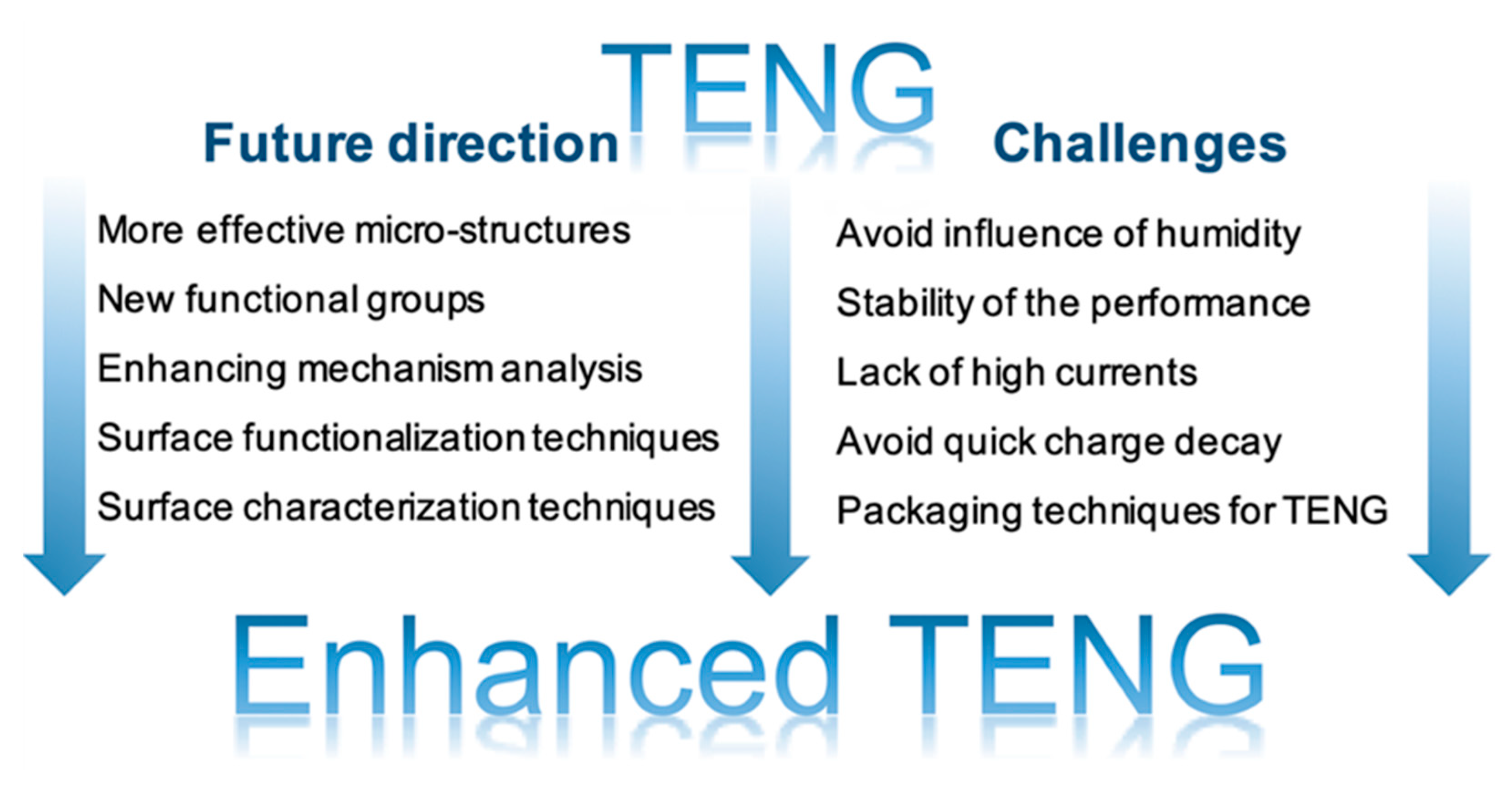
4. Summary and Perspectives

In this review, summarized approaches, including surface morphology and surface modification, to the enhancement of the TENG performance are summarized. In the first approach, various surface morphology engineering methods have been developed to improve the performance of TENGs. Soft lithography, Photolithography, and ultrafast laser patterning were applied to regulate the surface morphology of the triboelectric materials. These methods are physical methods that won’t change the chemical structure or chemical element of the material. The advantage of this method is the high selectivity of the material, and almost all the materials can be applied in surface morphology engineering. The drawback of this method is the limitation of the surface charge density due to the limitation of the contact area. The other approach is surface modification, which will change the structure or element of the material such as functional groups modification, ion injection, and elemental doping. The surface modification of the triboelectric materials can improve the limitation of the surface charge density, but not all materials are suitable or able to be modified with functional groups. Whether surface morphology engineering or surface modification engineering can enhance the output performance, It is decided by the physical and chemical properties of the material when choosing a suitable surface engineering method. Figure 12 shows the diagram indicating the future direction and challenges of enhanced TENG. The future directions include more effective micro-structures, new functional groups, enhancing mechanism analysis, surface functionalization techniques and surface characterization techniques. The challenges include influence of humidity, stability of the performance, lack of high currents, quick charge decay and suitable packaging techniques. To be more specific, a roadmap for future research is shown as following:
(1)
More studies need to be done to discuss the mechanisms of enhancing the TENG performance, and the mechanism study should be taken from the perspective of structure design and material science.
(2)
More micro/nano structures that can enhance the output performance need to be detected. Although there have been various micro/nano structures to apply in the triboelectric material, there are still many materials that lack a suitable surface structure for improving the output performance. Besides, more theoretical simulation and structural observation methods need to be developed.
(3)
More research on the enhancement of TENG by semiconductors. Most surface modifications focused on polymers as insulation materials where the charges accumulate on the surface of the material, and metals are used as the most common friction materials resulting in the output of the TENG. However, semiconductor is also important but still largely unexplored.
(4)
More practical surface engineering methods towards all modes of TENG. The TENG has wide applications in four modes. However, the surface engineering is mainly conducted in the contact-separation mode TENG. Hence, it is important to make the surface engineering practical.
(5)
More direct and effective methods to improve the power output of TENGs with the electron-accepting (tend to obtain a negative charge) or donating (tend to obtain a positive charge) ability of functional groups, increasing surface properties of both triboelectric materials. The properties of triboelectric materials should be designed when the difference in the surface potential of triboelectric materials charges is large.
(6)
Overcome the influence of humidity through the designed packaging techniques. Besides, it is important to stabilize the enhanced output performance of TENG and avoid quick charge decay. More importantly, the other limitation for TENG is the low current. More efforts still need to be put in for the commercialization of TENG.

Author Contributions

Conceptualization, Z.W. and X.S.; writing—original draft preparation, M.I.; writing—review and editing, J.J. All authors have read and agreed to the published version of the manuscript.

Funding

This work was funded by the National Natural Science Foundation of China (NSFC) (No. 61804103), the Suzhou Science and Technology Development Planning Project: Key Industrial Technology Innovation (No. SYG201924) and China Postdoctoral Science Foundation (No. 2021T140494).

Acknowledgments

Mervat Ibrahim would like to acknowledge the fund from the scholarship (CSC type A) under the joint program (Executive program between the Arab Republic of Egypt and China). The authors also acknowledge the support from the Collaborative Innovation Center of Suzhou Nano Science & Technology, the 111 Project and Joint International Research Laboratory of Carbon-Based Functional Materials and Devices.

Conflicts of Interest

The authors declare no conflict of interest.

References

  1. Yang, W.; Chen, J.; Jing, Q.; Yang, J.; Wen, X.; Su, Y.; Zhu, G.; Bai, P.; Wang, Z.L. 3D Stack Integrated Triboelectric Nanogenerator for Harvesting Vibration Energy. Adv. Funct. Mater. 2014, 24, 4090–4096. [Google Scholar] [CrossRef]
  2. Pourrahimi, A.M.; Olsson, R.T.; Hedenqvist, M.S. The Role of Interfaces in Polyethylene/Metal-Oxide Nanocomposites for Ultrahigh-Voltage Insulating Materials. Adv. Mater. 2018, 30, 1703624. [Google Scholar] [CrossRef] [PubMed]
  3. Zhu, G.; Yang, R.; Wang, S.; Wang, Z.L. Flexible High-Output Nanogenerator Based on Lateral ZnO Nanowire Array. Nano Lett. 2010, 10, 3151–3155. [Google Scholar] [CrossRef] [Green Version]
  4. Suzuki, Y.; Miki, D.; Edamoto, M.; Honzumi, M. A MEMS electret generator with electrostatic levitation for vibration-driven energy-harvesting applications. J. Micromech. Microeng. 2010, 20, 104002. [Google Scholar] [CrossRef]
  5. Xu, S.; Hansen, B.J.; Wang, Z.L. Piezoelectric-nanowire-enabled power source for driving wireless microelectronics. Nat. Commun. 2010, 1, 93. [Google Scholar] [CrossRef]
  6. Kumar, B.; Lee, K.Y.; Park, H.-K.; Chae, S.J.; Lee, Y.H.; Kim, S.-W. Controlled Growth of Semiconducting Nanowire, Nanowall, and Hybrid Nanostructures on Graphene for Piezoelectric Nanogenerators. ACS Nano 2011, 5, 4197–4204. [Google Scholar] [CrossRef] [PubMed]
  7. Khan, A.; Abbasi, M.A.; Hussain, M.; Ibupoto, Z.H.; Wissting, J.; Nur, O.; Willander, M. Piezoelectric nanogenerator based on zinc oxide nanorods grown on textile cotton fabric. Appl. Phys. Lett. 2012, 101, 193506. [Google Scholar] [CrossRef]
  8. Yang, Y.; Pradel, K.C.; Jing, Q.; Wu, J.M.; Zhang, F.; Zhou, Y.; Zhang, Y.; Wang, Z.L. Thermoelectric Nanogenerators Based on Single Sb-Doped ZnO Micro/Nanobelts. ACS Nano 2012, 6, 6984–6989. [Google Scholar] [CrossRef]
  9. Wang, X. Piezoelectric nanogenerators—Harvesting ambient mechanical energy at the nanometer scale. Nano Energy 2012, 1, 13–24. [Google Scholar] [CrossRef]
  10. Yang, Y.; Guo, W.; Pradel, K.C.; Zhu, G.; Zhou, Y.; Zhang, Y.; Hu, Y.; Lin, L.; Wang, Z.L. Pyroelectric Nanogenerators for Harvesting Thermoelectric Energy. Nano Lett. 2012, 12, 2833–2838. [Google Scholar] [CrossRef] [PubMed]
  11. Fan, F.-R.; Tian, Z.-Q.; Lin Wang, Z. Flexible triboelectric generator. Nano Energy 2012, 1, 328–334. [Google Scholar] [CrossRef]
  12. Wang, Z.L. Triboelectric Nanogenerators as New Energy Technology for Self-Powered Systems and as Active Mechanical and Chemical Sensors. ACS Nano 2013, 7, 9533–9557. [Google Scholar] [CrossRef] [PubMed]
  13. Whiter, R.A.; Narayan, V.; Kar-Narayan, S. A Scalable Nanogenerator Based on Self-Poled Piezoelectric Polymer Nanowires with High Energy Conversion Efficiency. Adv. Energy Mater. 2014, 4, 1400519. [Google Scholar] [CrossRef] [Green Version]
  14. Crossley, S.; Kar-Narayan, S. Energy harvesting performance of piezoelectric ceramic and polymer nanowires. Nanotechnology 2015, 26, 344001. [Google Scholar] [CrossRef] [PubMed] [Green Version]
  15. Zhao, J.; Li, Y.; Yang, G.; Jiang, K.; Lin, H.; Ade, H.; Ma, W.; Yan, H. Efficient organic solar cells processed from hydrocarbon solvents. Nat. Energy 2016, 1, 15027. [Google Scholar] [CrossRef]
  16. Invernizzi, F.; Dulio, S.; Patrini, M.; Guizzetti, G.; Mustarelli, P. Energy harvesting from human motion: Materials and techniques. Chem. Soc. Rev. 2016, 45, 5455–5473. [Google Scholar] [CrossRef] [PubMed]
  17. Boughey, C.; Davies, T.; Datta, A.; Whiter, R.A.; Sahonta, S.-L.; Kar-Narayan, S. Vertically aligned zinc oxide nanowires electrodeposited within porous polycarbonate templates for vibrational energy harvesting. Nanotechnology 2016, 27, 28LT02. [Google Scholar] [CrossRef] [Green Version]
  18. Wang, Z.L. On Maxwell’s displacement current for energy and sensors: The origin of nanogenerators. Mater. Today 2017, 20, 74–82. [Google Scholar] [CrossRef]
  19. Ahmed, A.; Hassan, I.; Hedaya, M.; El-Yazid, T.A.; Zu, J.; Wang, Z.L. Farms of triboelectric nanogenerators for harvesting wind energy: A potential approach towards green energy. Nano Energy 2017, 36, 21–29. [Google Scholar] [CrossRef]
  20. Wang, Z.L. Nanogenerators, self-powered systems, blue energy, piezotronics and piezo-phototronics—A recall on the original thoughts for coining these fields. Nano Energy 2018, 54, 477–483. [Google Scholar] [CrossRef]
  21. Chen, J.; Wang, Z.L. Reviving Vibration Energy Harvesting and Self-Powered Sensing by a Triboelectric Nanogenerator. Joule 2017, 1, 480–521. [Google Scholar] [CrossRef]
  22. Wang, Z.L. Triboelectric nanogenerators as new energy technology and self-powered sensors—Principles, problems and perspectives. Faraday Discuss. 2014, 176, 447–458. [Google Scholar] [CrossRef] [PubMed]
  23. Wen, Z.; Shen, Q.; Sun, X. Nanogenerators for Self-Powered Gas Sensing. Nano-Micro Lett. 2017, 9, 1–19. [Google Scholar] [CrossRef] [PubMed]
  24. Cheng, P.; Liu, Y.; Wen, Z.; Shao, H.; Wei, A.; Xie, X.; Chen, C.; Yang, Y.; Peng, M.; Zhuo, Q.; et al. Atmospheric pressure difference driven triboelectric nanogenerator for efficiently harvesting ocean wave energy. Nano Energy 2018, 54, 156–162. [Google Scholar] [CrossRef]
  25. Huang, L.-B.; Xu, W.; Tian, W.; Han, J.-C.; Zhao, C.-H.; Wu, H.-L.; Hao, J. Ultrasonic-assisted ultrafast fabrication of polymer nanowires for high performance triboelectric nanogenerators. Nano Energy 2020, 71, 104593. [Google Scholar] [CrossRef]
  26. Wang, M.; Pan, J.; Wang, M.; Sun, T.; Ju, J.; Tang, Y.; Wang, J.; Mao, W.; Wang, Y.; Zhu, J. High-Performance Triboelectric Nanogenerators Based on a Mechanoradical Mechanism. ACS Sustain. Chem. Eng. 2020, 8, 3865–3871. [Google Scholar] [CrossRef]
  27. Tantraviwat, D.; Buarin, P.; Suntalelat, S.; Sripumkhai, W.; Pattamang, P.; Rujijanagul, G.; Inceesungvorn, B. Highly dispersed porous polydimethylsiloxane for boosting power-generating performance of triboelectric nanogenerators. Nano Energy 2020, 67, 104214. [Google Scholar] [CrossRef]
  28. Kim, J.; Ryu, H.; Lee, J.H.; Khan, U.; Kwak, S.S.; Yoon, H.; Kim, S. High Permittivity CaCu3Ti4O12 Particle-Induced Internal Polarization Amplification for High Performance Triboelectric Nanogenerators. Adv. Energy Mater. 2020, 10, 1903524. [Google Scholar] [CrossRef]
  29. Yan, S.; Dong, K.; Lu, J.; Song, W.; Xiao, R. Amphiphobic triboelectric nanogenerators based on silica enhanced thermoplastic polymeric nanofiber membranes. Nanoscale 2020, 12, 4527–4536. [Google Scholar] [CrossRef]
  30. Rodrigues, C.; Nunes, D.; Clemente, D.; Mathias, N.; Correia, J.M.; Rosa-Santos, P.; Taveira-Pinto, F.; Morais, T.; Pereira, A.; Ventura, J. Emerging triboelectric nanogenerators for ocean wave energy harvesting: State of the art and future perspectives. Energy Environ. Sci. 2020, 13, 2657–2683. [Google Scholar] [CrossRef]
  31. Gao, Q.; Li, Y.; Xie, Z.; Yang, W.; Wang, Z.; Yin, M.; Lu, X.; Cheng, T.; Wang, Z.L. Robust Triboelectric Nanogenerator with Ratchet-like Wheel-Based Design for Harvesting of Environmental Energy. Adv. Mater. Technol. 2019, 5, 1900801. [Google Scholar] [CrossRef]
  32. Shi, K.; Zou, H.; Sun, B.; Jiang, P.; He, J.; Huang, X. Dielectric Modulated Cellulose Paper/PDMS-Based Triboelectric Nanogenerators for Wireless Transmission and Electropolymerization Applications. Adv. Funct. Mater. 2019, 30, 1904536. [Google Scholar] [CrossRef]
  33. Zhang, Y.; Wu, J.; Cui, S.; Wei, W.; Chen, W.; Pang, R.; Wu, Z.; Mi, L. Organosulfonate Counteranions—A Trapped Coordination Polymer as a High-Output Triboelectric Nanogenerator Material for Self-Powered Anticorrosion. Chem.—A Eur. J. 2020, 26, 584–591. [Google Scholar] [CrossRef] [PubMed]
  34. Khandelwal, G.; Raj, N.P.M.J.; Kim, S. Zeolitic Imidazole Framework: Metal–Organic Framework Subfamily Members for Triboelectric Nanogenerators. Adv. Funct. Mater. 2020, 30, 1910162. [Google Scholar] [CrossRef]
  35. Khandelwal, G.; Raj, N.P.M.J.; Kim, S.-J. ZIF-62: A mixed linker metal–organic framework for triboelectric nanogenerators. J. Mater. Chem. A 2020, 8, 17817–17825. [Google Scholar] [CrossRef]
  36. Cui, X.; Zhang, Y.; Hu, G.; Zhang, L.; Zhang, Y. Dynamical charge transfer model for high surface charge density triboelectric nanogenerators. Nano Energy 2020, 70, 104513. [Google Scholar] [CrossRef]
  37. Li, Y.; Zheng, W.; Zhang, H.; Wang, H.; Cai, H.; Zhang, Y.; Yang, Z. Electron transfer mechanism of graphene/Cu heterostructure for improving the stability of triboelectric nanogenerators. Nano Energy 2020, 70, 104540. [Google Scholar] [CrossRef]
  38. Guo, Y.; Cao, Y.; Chen, Z.; Li, R.; Gong, W.; Yang, W.; Zhang, Q.; Wang, H. Fluorinated metal-organic framework as bifunctional filler toward highly improving output performance of triboelectric nanogenerators. Nano Energy 2020, 70, 104517. [Google Scholar] [CrossRef]
  39. Zhou, L.; Liu, D.; Wang, J.; Wang, Z.L. Triboelectric nanogenerators: Fundamental physics and potential applications. Friction 2020, 8, 481–506. [Google Scholar] [CrossRef]
  40. Wang, Y.; Duan, J.; Yang, X.; Liu, L.; Zhao, L.; Tang, Q. The unique dielectricity of inorganic perovskites toward high-performance triboelectric nanogenerators. Nano Energy 2020, 69, 104418. [Google Scholar] [CrossRef]
  41. Feng, Y.; Zheng, Y.; Ma, S.; Wang, D.; Zhou, F.; Liu, W. High output polypropylene nanowire array triboelectric nanogenerator through surface structural control and chemical modification. Nano Energy 2016, 19, 48–57. [Google Scholar] [CrossRef]
  42. Cao, V.A.; Lee, S.; Kim, M.; Alam, M.; Park, P.; Nah, J. Output power density enhancement of triboelectric nanogenerators via ferroelectric polymer composite interfacial layers. Nano Energy 2020, 67, 104300. [Google Scholar] [CrossRef]
  43. Zhao, P.; Soin, N.; Kumar, A.; Shi, L.; Guan, S.; Tsonos, C.; Yu, Z.; Ray, S.C.; McLaughlin, J.A.; Zhu, Z.; et al. Expanding the portfolio of tribo-positive materials: Aniline formaldehyde condensates for high charge density triboelectric nanogenerators. Nano Energy 2020, 67, 104291. [Google Scholar] [CrossRef]
  44. Xu, S.; Ding, W.; Guo, H.; Wang, X.; Wang, Z.L. Boost the Performance of Triboelectric Nanogenerators through Circuit Oscillation. Adv. Energy Mater. 2019, 9, 1900772. [Google Scholar] [CrossRef]
  45. Stanford, M.G.; Li, J.; Chyan, Y.; Wang, Z.; Wang, W.; Tour, J.M. Laser-Induced Graphene Triboelectric Nanogenerators. ACS Nano 2019, 13, 7166–7174. [Google Scholar] [CrossRef] [PubMed]
  46. Šutka, A.; Mālnieks, K.; Lapčinskis, L.; Kaufelde, P.; Linarts, A.; Bērziņa, A.; Zābels, R.; Jurķāns, V.; Gorņevs, I.; Blūms, J.; et al. The role of intermolecular forces in contact electrification on polymer surfaces and triboelectric nanogenerators. Energy Environ. Sci. 2019, 12, 2417–2421. [Google Scholar] [CrossRef]
  47. Gao, L.; Chen, X.; Lu, S.; Zhou, H.; Xie, W.; Chen, J.; Qi, M.; Yu, H.; Mu, X.; Wang, Z.L.; et al. Triboelectric Nanogenerators: Enhancing the Output Performance of Triboelectric Nanogenerator via Grating-Electrode-Enabled Surface Plasmon Excitation (Adv. Energy Mater. 44/2019). Adv. Energy Mater. 2019, 9, 1970177. [Google Scholar] [CrossRef]
  48. Zhao, X.J.; Zhu, G.; Wang, Z.L. Coplanar Induction Enabled by Asymmetric Permittivity of Dielectric Materials for Mechanical Energy Conversion. ACS Appl. Mater. Interfaces 2015, 7, 6025–6029. [Google Scholar] [CrossRef] [PubMed]
  49. Shin, S.-H.; Bae, Y.E.; Moon, H.K.; Kim, J.; Choi, S.-H.; Kim, Y.; Yoon, H.J.; Lee, M.H.; Nah, J. Formation of Triboelectric Series via Atomic-Level Surface Functionalization for Triboelectric Energy Harvesting. ACS Nano 2017, 11, 6131–6138. [Google Scholar] [CrossRef]
  50. Liu, C.-Y.; Bard, A.J. Electrons on dielectrics and contact electrification. Chem. Phys. Lett. 2009, 480, 145–156. [Google Scholar] [CrossRef]
  51. Kim, Y.J.; Lee, J.; Park, S.; Park, C.; Park, C.; Choi, H.J. Effect of the relative permittivity of oxides on the performance of triboelectric nanogenerators. RSC Adv. 2017, 7, 49368–49373. [Google Scholar] [CrossRef] [Green Version]
  52. Żenkiewicz, M.; Żuk, T.; Markiewicz, E. Triboelectric series and electrostatic separation of some biopolymers. Polym. Test. 2015, 42, 192–198. [Google Scholar] [CrossRef]
  53. Lee, B.-Y.; Kim, S.-U.; Kang, S.; Lee, S.-D. Transparent and flexible high power triboelectric nanogenerator with metallic nanowire-embedded tribonegative conducting polymer. Nano Energy 2018, 53, 152–159. [Google Scholar] [CrossRef]
  54. Chen, J.; Guo, H.; He, X.; Liu, G.; Xi, Y.; Shi, H.; Hu, C. Enhancing Performance of Triboelectric Nanogenerator by Filling High Dielectric Nanoparticles into Sponge PDMS Film. ACS Appl. Mater. Interfaces 2016, 8, 736–744. [Google Scholar] [CrossRef] [PubMed]
  55. Lin, W.-C.; Lee, S.-H.; Karakachian, M.; Yu, B.-Y.; Chen, Y.-Y.; Lin, Y.-C.; Kuo, C.-H.; Shyue, J.-J. Tuning the surface potential of gold substrates arbitrarily with self-assembled monolayers with mixed functional groups. Phys. Chem. Chem. Phys. 2009, 11, 6199–6204. [Google Scholar] [CrossRef] [PubMed]
  56. Lin, Z.-H.; Xie, Y.; Yang, Y.; Wang, S.; Zhu, G.; Wang, Z.L. Enhanced Triboelectric Nanogenerators and Triboelectric Nanosensor Using Chemically Modified TiO2 Nanomaterials. ACS Nano 2013, 7, 4554–4560. [Google Scholar] [CrossRef] [PubMed]
  57. Zhu, G.; Lin, Z.-H.; Jing, Q.; Bai, P.; Pan, C.; Yang, Y.; Zhou, Y.; Wang, Z.L. Toward Large-Scale Energy Harvesting by a Nanoparticle-Enhanced Triboelectric Nanogenerator. Nano Lett. 2013, 13, 847–853. [Google Scholar] [CrossRef]
  58. Niu, S.; Wang, S.; Liu, Y.; Zhou, Y.; Lin, L.; Hu, Y.; Pradel, K.C.; Wang, Z.L. A theoretical study of grating structured triboelectric nanogenerators. Energy Environ. Sci. 2014, 7, 2339–2349. [Google Scholar] [CrossRef]
  59. Jeong, C.K.; Baek, K.M.; Niu, S.; Nam, T.W.; Hur, Y.H.; Park, D.Y.; Hwang, G.-T.; Byun, M.; Wang, Z.L.; Jung, Y.S.; et al. Topographically-Designed Triboelectric Nanogenerator via Block Copolymer Self-Assembly. Nano Lett. 2014, 14, 7031–7038. [Google Scholar] [CrossRef] [PubMed]
  60. Wang, S.; Xie, Y.; Niu, S.; Lin, L.; Liu, C.; Zhou, Y.S.; Wang, Z.L. Maximum Surface Charge Density for Triboelectric Nanogenerators Achieved by Ionized-Air Injection: Methodology and Theoretical Understanding. Adv. Mater. 2014, 26, 6720–6728. [Google Scholar] [CrossRef]
  61. Kim, D.; Jeon, S.-B.; Kim, J.Y.; Seol, M.-L.; Kim, S.O.; Choi, Y.-K. High-performance nanopattern triboelectric generator by block copolymer lithography. Nano Energy 2015, 12, 331–338. [Google Scholar] [CrossRef]
  62. Wang, S.; Zi, Y.; Zhou, Y.S.; Li, S.; Fan, F.; Lin, L.; Wang, Z.L. Molecular surface functionalization to enhance the power output of triboelectric nanogenerators. J. Mater. Chem. A 2016, 4, 3728–3734. [Google Scholar] [CrossRef]
  63. Wang, H.S.; Jeong, C.K.; Seo, M.-H.; Joe, D.; Han, J.H.; Yoon, J.-B.; Lee, K.J. Performance-enhanced triboelectric nanogenerator enabled by wafer-scale nanogrates of multistep pattern downscaling. Nano Energy 2017, 35, 415–423. [Google Scholar] [CrossRef]
  64. Zhu, G.; Pan, C.; Guo, W.; Chen, C.-Y.; Zhou, Y.; Yu, R.; Wang, Z.L. Triboelectric-Generator-Driven Pulse Electrodeposition for Micropatterning. Nano Lett. 2012, 12, 4960–4965. [Google Scholar] [CrossRef]
  65. Fan, F.-R.; Lin, L.; Zhu, G.; Wu, W.; Zhang, R.; Wang, Z.L. Transparent Triboelectric Nanogenerators and Self-Powered Pressure Sensors Based on Micropatterned Plastic Films. Nano Lett. 2012, 12, 3109–3114. [Google Scholar] [CrossRef] [Green Version]
  66. Song, G.; Kim, Y.; Yu, S.; Kim, M.-O.; Park, S.-H.; Cho, S.M.; Velusamy, D.B.; Cho, S.H.; Kim, K.L.; Kim, J.; et al. Molecularly Engineered Surface Triboelectric Nanogenerator by Self-Assembled Monolayers (METS). Chem. Mater. 2015, 27, 4749–4755. [Google Scholar] [CrossRef]
  67. Wang, S.; Lin, L.; Wang, Z.L. Nanoscale Triboelectric-Effect-Enabled Energy Conversion for Sustainably Powering Portable Electronics. Nano Lett. 2012, 12, 6339–6346. [Google Scholar] [CrossRef] [PubMed] [Green Version]
  68. Seung, W.; Yoon, H.J.; Kim, T.Y.; Ryu, H.; Kim, J.; Lee, J.H.; Lee, J.H.; Kim, S.; Park, Y.K.; Park, Y.J.; et al. Boosting Power-Generating Performance of Triboelectric Nanogenerators via Artificial Control of Ferroelectric Polarization and Dielectric Properties. Adv. Energy Mater. 2017, 7, 1600988. [Google Scholar] [CrossRef]
  69. Wu, C.; Kim, T.W.; Choi, H.Y. Reduced graphene-oxide acting as electron-trapping sites in the friction layer for giant triboelectric enhancement. Nano Energy 2017, 32, 542–550. [Google Scholar] [CrossRef]
  70. Wang, Z.L.; Wang, A.C. On the origin of contact-electrification. Mater. Today 2019, 30, 34–51. [Google Scholar] [CrossRef]
  71. Elahi, H.; Mughal, M.R.; Eugeni, M.; Qayyum, F.; Israr, A.; Ali, A.; Munir, K.; Praks, J.; Gaudenzi, P. Characterization and Implementation of a Piezoelectric Energy Harvester Configuration: Analytical, Numerical and Experimental Approach. Integr. Ferroelectr. 2020, 212, 39–60. [Google Scholar] [CrossRef]
  72. Wang, Z.L. On the first principle theory of nanogenerators from Maxwell’s equations. Nano Energy 2020, 68, 104272. [Google Scholar] [CrossRef]
  73. Huang, T.; Lu, M.; Yu, H.; Zhang, Q.; Wang, H.; Zhu, M. Enhanced Power Output of a Triboelectric Nanogenerator Composed of Electrospun Nanofiber Mats Doped with Graphene Oxide. Sci. Rep. 2015, 5, srep13942. [Google Scholar] [CrossRef] [Green Version]
  74. Li, W.; Zhang, Y.; Liu, L.; Li, D.; Liao, L.; Pan, C. A high energy output nanogenerator based on reduced graphene oxide. Nanoscale 2015, 7, 18147–18151. [Google Scholar] [CrossRef]
  75. Park, S.-J.; Seol, M.-L.; Kim, D.; Jeon, S.-B.; Choi, Y.-K. Triboelectric nanogenerator with nanostructured metal surface using water-assisted oxidation. Nano Energy 2016, 21, 258–264. [Google Scholar] [CrossRef]
  76. Lee, J.H.; Yu, I.; Hyun, S.; Kim, J.K.; Jeong, U. Remarkable increase in triboelectrification by enhancing the conformable contact and adhesion energy with a film-covered pillar structure. Nano Energy 2017, 34, 233–241. [Google Scholar] [CrossRef]
  77. Zhao, L.; Zheng, Q.; Ouyang, H.; Li, H.; Yan, L.; Shi, B.; Li, Z. A size-unlimited surface microstructure modification method for achieving high performance triboelectric nanogenerator. Nano Energy 2016, 28, 172–178. [Google Scholar] [CrossRef]
  78. Zhang, H.; Yang, Y.; Su, Y.; Chen, J.; Adams, K.; Lee, S.; Hu, C.; Wang, Z.L. Triboelectric Nanogenerator for Harvesting Vibration Energy in Full Space and as Self-Powered Acceleration Sensor. Adv. Funct. Mater. 2014, 24, 1401–1407. [Google Scholar] [CrossRef]
  79. Cui, N.; Gu, L.; Lei, Y.; Liu, J.; Qin, Y.; Ma, X.-H.; Hao, Y.; Wang, Z.L. Dynamic Behavior of the Triboelectric Charges and Structural Optimization of the Friction Layer for a Triboelectric Nanogenerator. ACS Nano 2016, 10, 6131–6138. [Google Scholar] [CrossRef]
  80. Kaur, N.; Bahadur, J.; Panwar, V.; Singh, P.; Rathi, K.; Pal, K. Effective energy harvesting from a single electrode based triboelectric nanogenerator. Sci. Rep. 2016, 6, 38835. [Google Scholar] [CrossRef] [Green Version]
  81. Guo, H.; Li, T.; Cao, X.; Xiong, J.; Jie, Y.; Willander, M.; Cao, X.; Wang, N.; Wang, Z.L. Self-Sterilized Flexible Single-Electrode Triboelectric Nanogenerator for Energy Harvesting and Dynamic Force Sensing. ACS Nano 2017, 11, 856–864. [Google Scholar] [CrossRef] [PubMed]
  82. Zhang, X.-S.; Han, M.-D.; Wang, R.-X.; Zhu, F.-Y.; Li, Z.-H.; Wang, W.; Zhang, H. Frequency-Multiplication High-Output Triboelectric Nanogenerator for Sustainably Powering Biomedical Microsystems. Nano Lett. 2013, 13, 1168–1172. [Google Scholar] [CrossRef] [PubMed]
  83. Nafari, A.; Sodano, H.A. Surface morphology effects in a vibration based triboelectric energy harvester. Smart Mater. Struct. 2018, 27, 015029. [Google Scholar] [CrossRef]
  84. Gong, J.; Xu, B.; Tao, X. Breath Figure Micromolding Approach for Regulating the Microstructures of Polymeric Films for Triboelectric Nanogenerators. ACS Appl. Mater. Interfaces 2017, 9, 4988–4997. [Google Scholar] [CrossRef] [PubMed]
  85. Sun, J.-G.; Yang, T.N.; Kuo, I.-S.; Wu, J.-M.; Wang, C.-Y.; Chen, L.-J. A leaf-molded transparent triboelectric nanogenerator for smart multifunctional applications. Nano Energy 2017, 32, 180–186. [Google Scholar] [CrossRef] [Green Version]
  86. Rasel, M.S.U.; Park, J.Y. A sandpaper assisted micro-structured polydimethylsiloxane fabrication for human skin based triboelectric energy harvesting application. Appl. Energy 2017, 206, 150–158. [Google Scholar] [CrossRef]
  87. Jiang, L.; Wang, A.; Li, B.; Cui, T.; Lu, Y.-F. Electrons dynamics control by shaping femtosecond laser pulses in micro/nanofabrication: Modeling, method, measurement and application. Light. Sci. Appl. 2018, 7, 17134. [Google Scholar] [CrossRef] [PubMed] [Green Version]
  88. Malinauskas, M.; Žukauskas, A.; Hasegawa, S.; Hayasaki, Y.; Mizeikis, V.; Buividas, R.; Juodkazis, S. Ultrafast laser processing of materials: From science to industry. Light. Sci. Appl. 2016, 5, e16133. [Google Scholar] [CrossRef] [Green Version]
  89. Vorobyev, A.Y.; Guo, C.L. Direct femtosecond laser surface nano/microstructuring and its applications. Laser Photonics Rev. 2013, 7, 385–407. [Google Scholar] [CrossRef]
  90. Kim, D.; Tcho, I.-W.; Jin, I.K.; Park, S.-J.; Jeon, S.-B.; Kim, W.-G.; Cho, H.-S.; Lee, H.-S.; Jeoung, S.C.; Choi, Y.-K. Direct-laser-patterned friction layer for the output enhancement of a triboelectric nanogenerator. Nano Energy 2017, 35, 379–386. [Google Scholar] [CrossRef]
  91. Huang, J.; Fu, X.; Liu, G.; Xu, S.; Li, X.; Zhang, C.; Jiang, L. Micro/nano-structures-enhanced triboelectric nanogenerators by femtosecond laser direct writing. Nano Energy 2019, 62, 638–644. [Google Scholar] [CrossRef]
  92. Zhai, N.; Wen, Z.; Chen, X.; Wei, A.; Sha, M.; Fu, J.; Liu, Y.; Zhong, J.; Sun, X. Blue Energy Collection toward All-Hours Self-Powered Chemical Energy Conversion. Adv. Energy Mater. 2020, 10, 2001041. [Google Scholar] [CrossRef]
  93. Byun, K.-E.; Cho, Y.; Seol, M.; Kim, S.; Kim, S.-W.; Shin, H.-J.; Park, S.; Hwang, S.W. Control of Triboelectrification by Engineering Surface Dipole and Surface Electronic State. ACS Appl. Mater. Interfaces 2016, 8, 18519–18525. [Google Scholar] [CrossRef] [PubMed]
  94. Zhou, Y.S.; Liu, Y.; Zhu, G.; Lin, Z.-H.; Pan, C.; Jing, Q.; Wang, Z.L. In Situ Quantitative Study of Nanoscale Triboelectrification and Patterning. Nano Lett. 2013, 13, 2771–2776. [Google Scholar] [CrossRef] [PubMed] [Green Version]
  95. Shin, S.-H.; Kwon, Y.H.; Kim, Y.-H.; Jung, J.-Y.; Lee, M.H.; Nah, J. Triboelectric Charging Sequence Induced by Surface Functionalization as a Method to Fabricate High Performance Triboelectric Generators. ACS Nano 2015, 9, 4621–4627. [Google Scholar] [CrossRef]
  96. Busolo, T.; Ura, D.; Kim, S.K.; Marzec, M.M.; Bernasik, A.; Stachewicz, U.; Kar-Narayan, S. Surface potential tailoring of PMMA fibers by electrospinning for enhanced triboelectric performance. Nano Energy 2019, 57, 500–506. [Google Scholar] [CrossRef]
  97. Li, S.; Fan, Y.; Chen, H.; Nie, J.; Liang, Y.; Tao, X.; Zhang, J.; Chen, X.; Fu, E.; Wang, Z.L. Manipulating the triboelectric surface charge density of polymers by low-energy helium ion irradiation/implantation. Energy Environ. Sci. 2020, 13, 896–907. [Google Scholar] [CrossRef]
  98. Liu, L.; Tang, W.; Wang, Z.L. Inductively-coupled-plasma-induced electret enhancement for triboelectric nanogenerators. Nanotechnology 2016, 28, 035405. [Google Scholar] [CrossRef]
  99. Xu, L.; Bu, T.Z.; Yang, X.D.; Zhang, C.; Wang, Z.L. Ultrahigh charge density realized by charge pumping at ambient conditions for triboelectric nanogenerators. Nano Energy 2018, 49, 625–633. [Google Scholar] [CrossRef]
  100. Lin, Z.-H.; Cheng, G.; Lee, S.; Pradel, K.C.; Wang, Z.L. Harvesting Water Drop Energy by a Sequential Contact-Electrification and Electrostatic-Induction Process. Adv. Mater. 2014, 26, 4690–4696. [Google Scholar] [CrossRef]
  101. Babudri, F.; Farinola, G.M.; Naso, F.; Ragni, R. Fluorinated organic materials for electronic and optoelectronic applications: The role of the fluorine atom. Chem. Commun. 2007, 10, 1003–1022. [Google Scholar] [CrossRef] [PubMed]
  102. Shao, J.; Tang, W.; Jiang, T.; Chen, X.; Xu, L.; Chen, B.; Zhou, T.; Deng, C.R.; Wang, Z.L. A multi-dielectric-layered triboelectric nanogenerator as energized by corona discharge. Nanoscale 2017, 9, 9668–9675. [Google Scholar] [CrossRef]
  103. Kim, M.P.; Lee, Y.; Hur, Y.H.; Park, J.; Kim, J.; Lee, Y.; Ahn, C.W.; Song, S.W.; Jung, Y.S.; Ko, H. Molecular structure engineering of dielectric fluorinated polymers for enhanced performances of triboelectric nanogenerators. Nano Energy 2018, 53, 37–45. [Google Scholar] [CrossRef]
  104. Park, S.; Kim, H.; Vosgueritchian, M.; Cheon, S.; Kim, H.; Koo, J.H.; Kim, T.R.; Lee, S.; Schwartz, G.; Chang, H.; et al. Stretchable Energy-Harvesting Tactile Electronic Skin Capable of Differentiating Multiple Mechanical Stimuli Modes. Adv. Mater. 2014, 26, 7324–7332. [Google Scholar] [CrossRef]
  105. Lee, K.Y.; Chun, J.; Lee, J.-H.; Kim, K.N.; Kang, N.-R.; Kim, J.-Y.; Kim, M.H.; Shin, K.-S.; Gupta, M.K.; Baik, J.M.; et al. Hydrophobic Sponge Structure-Based Triboelectric Nanogenerator. Adv. Mater. 2014, 26, 5037–5042. [Google Scholar] [CrossRef] [PubMed]
  106. Thakur, V.K.; Tan, E.J.; Lin, M.-F.; Lee, P.S. Polystyrene grafted polyvinylidenefluoride copolymers with high capacitive performance. Polym. Chem. 2011, 2, 2000–2009. [Google Scholar] [CrossRef]
  107. Wang, C.C.; Chang, C.Y. Enhanced output performance and stability of triboelectric nanogenerators by employing silane-based self-assembled monolayers. J. Mater. Chem. C 2020, 8, 4542–4548. [Google Scholar] [CrossRef]
  108. Guo, Q.Z.; Yang, L.C.; Wang, R.C.; Liu, C.P. Tunable Work Function of MgxZn1-xO as a Viable Friction Material for a Triboelectric Nanogenerator. ACS Appl. Mater. Interfaces 2019, 11, 1420–1425. [Google Scholar] [CrossRef]
  109. Chen, S.-N.; Chen, C.-H.; Lin, Z.-H.; Tsao, Y.-H.; Liu, C.-P. On enhancing capability of tribocharge transfer of ZnO nanorod arrays by Sb doping for anomalous output performance improvement of triboelectric nanogenerators. Nano Energy 2018, 45, 311–318. [Google Scholar] [CrossRef]
  110. Kang, X.; Pan, C.; Chen, Y.; Pu, X. Boosting performances of triboelectric nanogenerators by optimizing dielectric properties and thickness of electrification layer. RSC Adv. 2020, 10, 17752–17759. [Google Scholar] [CrossRef]
  111. Chun, J.; Kim, J.W.; Jung, W.-S.; Kang, C.-Y.; Kim, S.-W.; Wang, Z.L.; Baik, J.M. Mesoporous pores impregnated with Au nanoparticles as effective dielectrics for enhancing triboelectric nanogenerator performance in harsh environments. Energy Environ. Sci. 2015, 8, 3006–3012. [Google Scholar] [CrossRef]
  112. Han, S.A.; Lee, J.H.; Seung, W.; Lee, J.; Kim, S.W.; Kim, J.H. Patchable and Implantable 2D Nanogenerator. Small 2021, 17, e1903519. [Google Scholar] [CrossRef]
  113. Mariappan, V.K.; Krishnamoorthy, K.; Pazhamalai, P.; Natarajan, S.; Sahoo, S.; Nardekar, S.S.; Kim, S.-J. Antimonene dendritic nanostructures: Dual-functional material for high-performance energy storage and harvesting devices. Nano Energy 2020, 77, 105248. [Google Scholar] [CrossRef]
  114. Seol, M.; Kim, S.; Cho, Y.; Byun, K.E.; Kim, H.; Kim, J.; Kim, S.K.; Kim, S.W.; Shin, H.J.; Park, S. Triboelectric Series of 2D Layered Materials. Adv. Mater. 2018, 30, e1801210. [Google Scholar] [CrossRef]
  115. Wu, C.; Kim, T.W.; Park, J.H.; Whan, K.T.; Shao, J.; Chen, X.; Wang, Z.L. Enhanced Triboelectric Nanogenerators Based on MoS2 Monolayer Nanocomposites Acting as Electron-Acceptor Layers. ACS Nano 2017, 11, 8356–8363. [Google Scholar] [CrossRef] [PubMed]
  116. Wen, R.; Guo, J.; Yu, A.; Zhang, K.; Kou, J.; Zhu, Y.; Zhang, Y.; Li, B.-W.; Zhai, J. Remarkably enhanced triboelectric nanogenerator based on flexible and transparent monolayer titania nanocomposite. Nano Energy 2018, 50, 140–147. [Google Scholar] [CrossRef]
Figure 1. Schematic diagram showing the Triboelectric Nanogenerator (TENG), surface engineering, and application [65,66,67,68,69]. Copyright, 2012 American Chemical Society. Copyright, 2012 American Chemical Society. Copyright, 2016 WILEY-VCH Verlag GmbH & Co. KGaA, Weinheim, Germany. Copyright, 2017 Elsevier Ltd., Amsterdam, The Netherlands.
Nanoenergyadv 01 00004 g001
Figure 2. (a) Schematic illustration of arch-shape based on TENG. (b) SEM images of pyramid and cubic patterns of polydimethylsiloxane (PDMS) with Al surface. (c) The electrical voltage and the current from each frequency of the TENG, which gives the total charges transferred in a half cycle [67] Copyright, 2012 American Chemical Society. (d) Structural design of the sandwich-shaped triboelectric nanogenerator. (e) The output performance of the sandwich-shape based on TENG with flat PDMS film, surface-nanostructured PDMS film, pyramids and V-shape grooves [82] Copyright, 2013 American Chemical Society. (f) Au nanopatterning process and fabrication process of TENGs by using block copolymer (BCP) lithography. (g) Open-circuit current and voltage comparison between Au nanopatterned and flat Au [61] Copyright, 2015 Elsevier Ltd.
Nanoenergyadv 01 00004 g002
Figure 3. (ac) Scanning electron microscope images of photolithography traditional patterned PDMS as a friction layer with (a) lines, (b) cubes, and (c) pyramids. (d) Triboelectric voltage and current with a flat surface and various patterned features device [65] Copyright, 2012 American Chemical Society.
Nanoenergyadv 01 00004 g003
Figure 4. (a) Fabrication process of PDMS by using a laser power of 29 mW. (b) Electrical output performance of LI-TENGs using laser power from 0 to 132 mW [90] Copyright, 2017 Elsevier Ltd. (c) Schematic illustration of TENGs by Femtosecond laser direct writing processes. (d) SEM images of Cu and PDMS films with micro/nano-stripes, cones and small/large size micro-bowls, structures. (e) Transferred charge density, voltage, and current density with and without various micro/nanostructures [91] Copyright, 2019 Elsevier Ltd.
Nanoenergyadv 01 00004 g004
Figure 5. (a) Schematic illustration of TENGs built using SAM layer based on Au films. (b) The output comparisons of TENG based on each thiol SAM functionalized Au films. (c) Fabrication process of TENG using silane -SAM modified SiO2. (d) the output of TENG with and without functionalized silica [62] Copyright, 2016 Royal Society of Chemistry. (e) Schematic illustration of TENG (inset figure shows the molecularly engineered surface by self-assembled monolayer (SAMs)). (f) Chemical structures of self-assembled monolayers (METS). (g) The voltage and current with and without METS [66] Copyright, 2015 American Chemical Society.
Nanoenergyadv 01 00004 g005
Figure 6. (a) Schematic illustration of the SAM-modified substrates from donor electron to acceptor electron layers. (b) Contact potential difference (CPD) analysis of each substrate. (c) Triboelectric potentials and CPD before contact of the different surfaces [93] Copyright, 2016 American Chemical Society. (d) The effect of surface modification on PET films with various contact pairs of the TENGs. (e) Voltage output and current densities of the contact pairs of the TENG [95] Copyright, 2015 American Chemical Society.
Nanoenergyadv 01 00004 g006
Figure 7. (a) Basic processes on FEP surface with ionized air injection. (b) The charge flow measurement in the FEP film during the ion injection. (c) The short-circuit charge density (ΔσSC) generated during the step-by-step ion injection process. (d) Open-circuit voltages of the TENG before and after the process of ion injection [60] Copyright, 2014 WILEY-VCH Verlag GmbH & Co. KGaA, Weinheim. (e,f) Schematic presentation of the ion irradiation process and corresponding to the molecular formula of Kapton structure change. (g,h) The output voltages and transferred charge densities of the pre and post -irradiation polymers with various materials [97] Copyright, 2016 Royal Society of Chemistry.
Nanoenergyadv 01 00004 g007
Figure 8. (a) Schematic illustration of TENGs built using fluorinated polymers with different numbers of fluorine. (b) Dielectric constants (εr) of different fluorinated polymers. (c) The output performance of TENG based on the effect of PEMA, PF, PTF, PPF, PHF, and number of fluorine units. (d) Effect of annealing temperature on electrical measurements [103] Copyright, 2019 Elsevier Ltd. (e) Schematic illustration of the TENG based on silane-SAM formation on a hydrated PDMS. (f) Output voltage, (g) current, and (h) charge density of the TENG with (F21, F17, and F13) compared to pristine PDMS [107] Copyright, 2020 Royal Society of Chemistry.
Nanoenergyadv 01 00004 g008
Figure 9. (a) Schematic illustration of TENGs composed of ZnO doping with Mg, triboelectric output current, and voltage of TENG of (b) pure ZnO (c) MgxZn1-xO films [108]. (d) Schematic diagram of the TENG based on ZnO doping by Sb. (e) TENG device mechanism of PDMS against ZnO nanorod arrays by Sb doping [109].
Nanoenergyadv 01 00004 g009
Figure 10. (a) Experimental design and diagram of PDMS sponge film-based TENG. (b) Electrical measurements of the device [54] Copyright, 2016 American Chemical Society; (c) Schematic diagram of (FC-TENG). (d) Output voltage and current of poled (PVDF-TrFE): BaTiO3 with PTFE and PFA as a triboelectric layer. (e) Output comparison with traditional TENGs [68] Copyright, 2016 WILEY-VCH Verlag GmbH & Co. KGaA, Weinheim.
Nanoenergyadv 01 00004 g010
Figure 11. (a) TENG made by a composite PI:rGO. (b) C-V curves of the Al/p-Si/PI/PI:rGO/PI/Al device [69] Copyright, 2017 Elsevier Ltd. (c) TENG with a MoS2-monolayer film as electron trapping layer. (d) Schematic of PI: MoS2 device [115] Copyright, 2017 American Chemical Society. (e) TENG with the PVDF/TOML nanocomposite films. (f) Maximum electrical output TENG device with 1.5% concentration of TOML [116] Copyright, 2018 Elsevier Ltd.
Nanoenergyadv 01 00004 g011
Figure 12. Diagram indicating the future direction and challenges of enhanced TENG.
Nanoenergyadv 01 00004 g012
Publisher’s Note: MDPI stays neutral with regard to jurisdictional claims in published maps and institutional affiliations.

