Article

Preparation of Antimony Tin Oxide Thin Film Using Green Synthesized Nanoparticles by E-Beam Technique for NO2 Gas Sensing

by
Chaitra Chandraiah
1,
Hullekere Mahadevaiah Kalpana
1,
Challaghatta Muniyappa Ananda
2 and
Madhusudan B. Kulkarni
3,*
1
Department of Electronics and Instrumentation Engineering, Siddaganga Institute of Technology, Tumakuru 572103, Karnataka, India
2
Aerospace Electronics and Systems Division, CSIR, National Aerospace Laboratories, Bengaluru 560017, Karnataka, India
3
Department of Medical Physics, University of Wisconsin-Madison, Madison, WI 53705, USA
*
Author to whom correspondence should be addressed.
Micro 2024, 4(3), 401-411; https://doi.org/10.3390/micro4030025
Submission received: 23 May 2024 / Revised: 13 June 2024 / Accepted: 20 June 2024 / Published: 21 June 2024
(This article belongs to the Special Issue Advances in Micro- and Nanomaterials: Synthesis and Applications)

Abstract

:
This work delves into the preparation of ATO thin films and their characterization, fabrication, and calibration of a NO2 gas sensor, as well as the development of the packaged sensor. ATO thin films were prepared by e-beam evaporation using green synthesized ATO nanomaterials on different substrates and annealed at 500 and 600 °C for one hour. The structural and morphological properties of the developed thin films were studied using scanning electron microscopy (SEM), transmission electron microscopy (TEM), and X-ray diffraction (XRD) techniques. An orthorhombic SnO2 crystal structure was recognized through XRD analysis. The granular-shaped nanoparticles were revealed through SEM and TEM images. The films annealed at 600 °C exhibited improved crystallinity. ATO films prepared on normal 5 µm interdigitated electrodes (IDEs) and annealed at 600 °C exhibited a response of 10.31 ± 0.25 with an optimum temperature of 200 °C for a 4.8 ppm NO2 gas concentration. The packaged NO2 gas sensor developed using IDEs with a microheater demonstrated an improved response of 16.20 ± 0.25 for 4.8 ppm of NO2 gas.

1. Introduction

During the combustion process of automobile engines, thermal power plants, furnaces, and home heaters, NO2 gas is released into the atmosphere, which is hazardous and causes severe human health problems [1,2,3,4,5]. The threshold limit of NO2 gas in the atmosphere is 25 ppm [6]. If any human consumes a lower concentration of NO2 gas for a longer time, they will suffer from respiratory disorders [7,8,9]. Therefore, a sensor that detects low concentrations of NO2 gas is an urgent need to protect the lives of individuals.
Solid-state materials are widely used in the fabrication of gas sensors. Depending on their sensing mechanism, they are classified as solid electrolyte, semiconductor, and catalytic combustion gas sensors [10]. Among these, semiconductor-based metal oxide nanomaterials are widely utilized for thin-film gas sensor fabrication because of their unique microstructures. The enhanced performance parameters of nanostructured thin-film sensors are due to the increased gas species adsorption on their surface. Metal oxide-based gas sensors are widely employed in environmental monitoring applications. There are numerous investigations on thin-film metal oxide nanomaterial-based gas sensors that have been reported by various researchers. Metal oxide materials such as tin oxide (SnO2), indium oxide (In2O3), zinc oxide (ZnO), and tungsten trioxide (WO3) were used in the preparation of thin-film NO2 gas sensors [3,8]. Among these, SnO2 is widely used because of its excellent crystallinity, thermal stability, and customizable morphology.
The addition of antimony as a dopant into the tin oxide enhances the gas sensor’s electrical conductivity and hence improves the sensitivity, stability, and selectivity [11]. According to the recent literature, antimony may cause risk to occupational health, and hence, authors have advised using it with constant vigilance and observation [12]. Thin films of ATO are prepared using various physical as well as chemical methods, such as thermal deposition, spin coating, sol-gel, flash evaporation, spray pyrolysis, and e-beam evaporation methods.
Further, the summary of NO2 gas sensor performance parameters developed by various researchers is listed in Table 1. As mentioned in Table 1, the response of the WO3 nanomaterial-based gas sensor prepared by [13] using the thermal evaporation method exhibited a response of four at an operating temperature of 250 °C. A SrTi0.85Fe00.15O3 nanomaterial-based gas sensor prepared by [14] using an E-beam evaporation method exhibited a response of four with a response/recovery time of 15 s/35 s at an operating temperature of 260 °C. A Pd:MoO3 nanomaterial-based gas sensor prepared by [15] using the chemical spray pyrolysis method exhibited a response of 5.5% with a response/recovery time of 11 s/76 s at an operating temperature of 200 °C towards 5 ppm of NO2 gas. However, this work utilized green synthesized ATO nanoparticles, and their thin films were prepared by the E-beam evaporation method for the development of a NO2 gas sensor which exhibited a response of 16.20 with a response/recovery time of 285 s/510 s at an operating temperature of 200 °C towards 4.8 ppm of NO2 gas.
In the present work, green synthesis of ATO nanoparticles has been carried out by the method of combustion of T. bellirica seed extract as fuel in the process, and its detailed experimental procedure is published in the literature [16]. The combustion method is preferred because of its advantages such as ease of synthesis and the ability to produce highly purified nanoparticles in large quantities. The thin films were prepared utilizing the e-beam evaporation technique. This method of deposition is utilized because of its many advantages, such as uniformity in deposition, which can be achieved at low temperatures, non-toxicity with evaporation, good adhesion over substrates, ease of control over the microstructures, and better material utilization characteristics. ATO thin films were prepared on silicon wafers, IDEs, and microheater-based IDEs, and the influence of the annealing temperature on the microstructural, morphological, and electrical properties has been reported. Using microheater-based IDEs, the fabrication of a thin-film-based NO2 gas sensor is carried out. This fabricated sensor is packaged, and gas sensing measurement is performed using a calibration setup. The ATO nanomaterial-based fabricated sensor showed an improved response for NO2 gas.

2. Materials and Methods

2.1. Preparation of ATO Films Using E-Beam Evaporation

Before the film deposition, the stainless steel-walled vacuum chamber was cleaned with a detergent cleaning process by which additional gases and water vapor were desorbed at each pumping cycle. Additionally, the graphite crucibles and substrate were cleaned using isopropyl alcohol and acetone to remove the impurities and water molecules before being placed in the vacuum chamber. The synthesized nanoparticles of ATO were used to prepare thin films. These nanoparticles were coated on silicon wafers and die-containing IDE substrates using the e-beam deposition method to perform various studies. The nanoparticles were filled in a graphite crucible and the chamber was evacuated to a high vacuum with pressure of 10−5 mbar by a rotary–diffusion pump combination. The accelerating voltage of the electron beam process is 5 KV. The substrate-to-source distance was maintained at 13 cm before depositing on the substrate (Si wafer/IDE). The optimized process parameters of deposition are listed in Table 2. To study the changes in the film surface structure, morphology, and electrical properties, they were post-annealed at 500 °C and 600 °C under vacuum conditions for 1 h. The thickness of the film was optimized after various experiments, and it was noticed that the thickness of films has a great influence on the sensor properties.

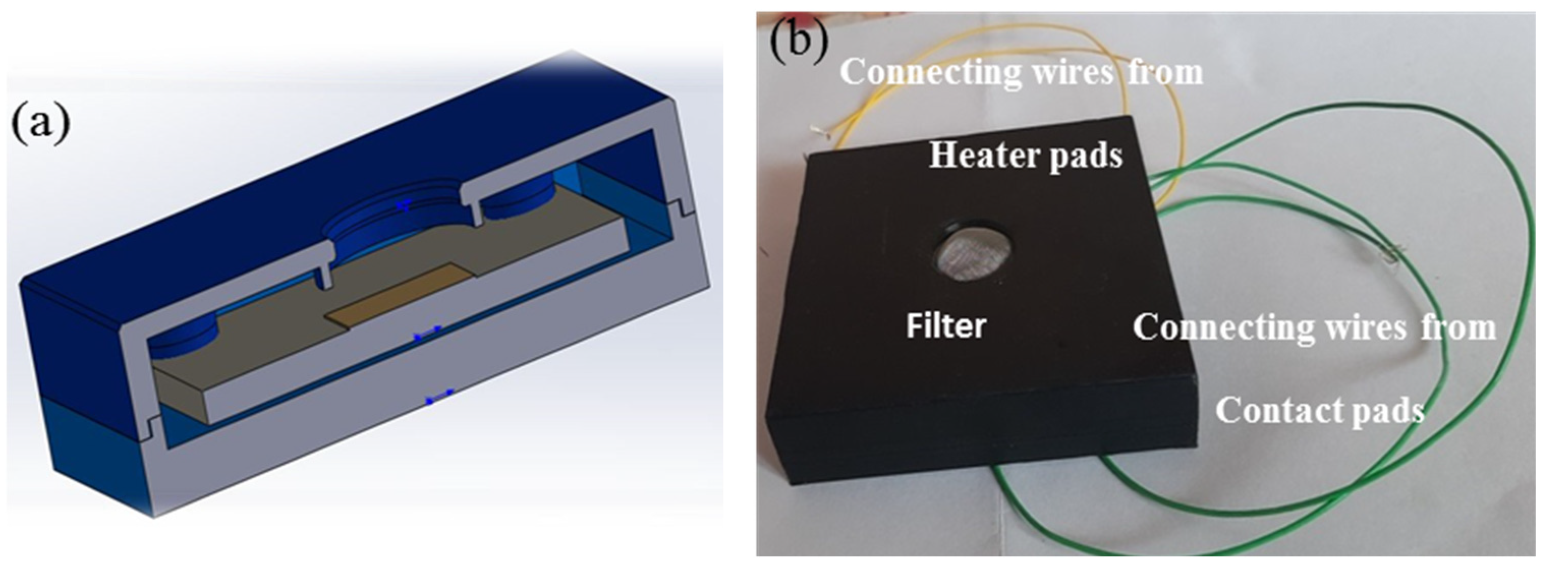
2.2. Fabrication and Packaging of ATO Film-Based NO2 Gas Sensor

The NO2 gas sensor was fabricated by depositing ATO thin films on an IDE with a microheater. The deposition was carried out by covering the IDE with an appropriate mechanical mask and using optimum E-beam evaporation parameters, as listed in Table 2. Post-deposition annealing was carried out at 600 °C for one hour. Solid Works 2022 software was used to design the mechanical housing for the sensor. This software is utilized to design the 3D printing of packaged sensors. Figure 1a,b display the packaged design of the sensor and the developed NO2 gas sensor, respectively. The filter of the sensor consists of mesh made up of stainless steel (SS304), which has pores with a size of 100 µm. The gas is passed through this filter to eliminate impurities present in the gas samples and air, as well as to reduce moisture. The yellow- and green-colored wires are from the microheater and IDE contact pads for measurements of sensor characteristics, respectively, and are supplied to the power source. Studies on the NO2 gas sensing of the developed sensor are carried out using a calibration setup.

2.3. Material Characterization

In this work, XRD was used to examine the structural properties of the prepared ATO thin films (model: Rigaku, Cu-kα, The Woodlands, TX 77381, USA). The surface morphological feature was examined by SEM (model: Carl Zeiss, ultra-55, Baden-Württemberg, Germany). The particle size and structure were investigated via TEM (model: FEI, Titan Themis 3391, Thermo Fisher Scientific, Waltham, MA 02451 USA). The temperature of the microheater was tracked using an SC5200 microscope setup.

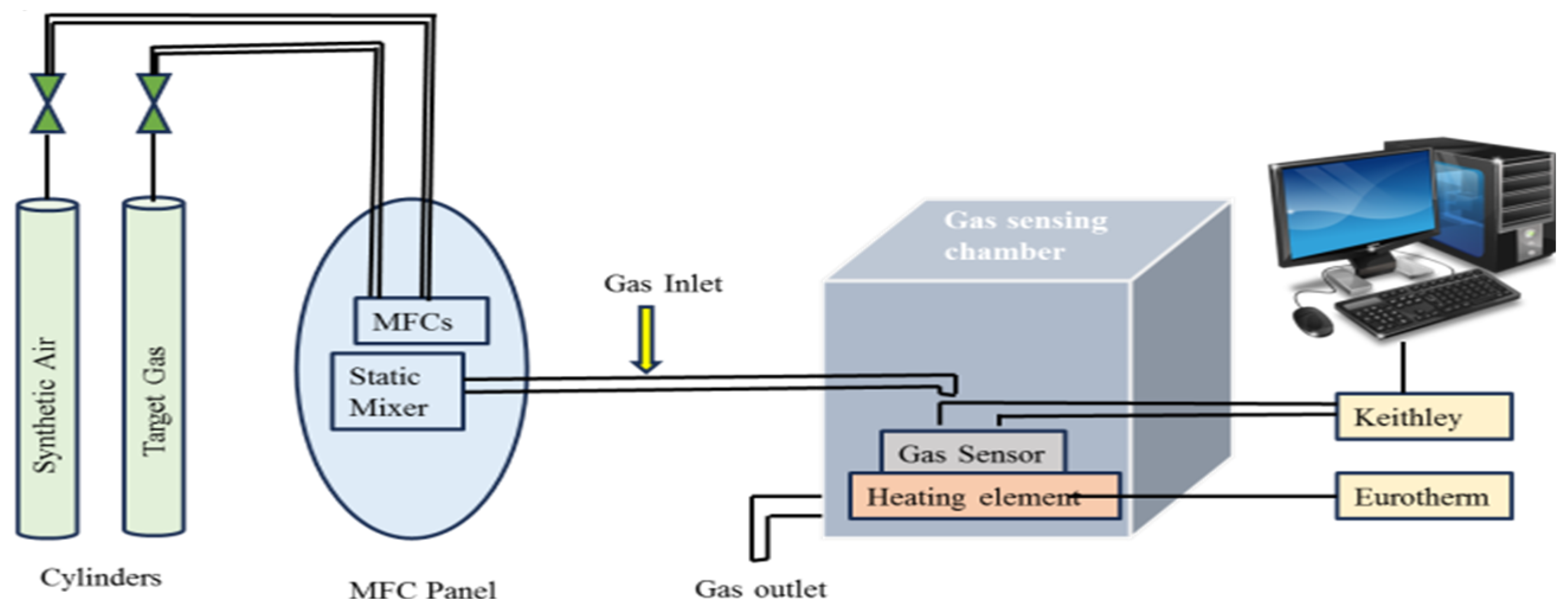
2.4. Gas Sensing Characterization of ATO Thin Films Prepared on IDEs Using Gas Calibration Setup

The schematic diagram of the gas sensor calibration setup is shown in Figure 2. The experimental procedures of the gas calibration setup are discussed in the literature [16]. The ATO thin film deposited on the IDE was placed on a graphite-based chuck with a temperature controller inside the gas chamber. The synthetic air (typically a mixture of oxygen and argon with 99.99% purity) and NO2 gas flows were controlled inside the gas chamber using MFCs (mass flow controllers). The sensor response is defined by [Rg − Ra)/Ra × 100], where Rg is the resistance of the film at a full concentration of the gas purge and Ra is the resistance of the film in a synthetic air atmosphere.

3. Results and Discussions

The structural, morphological, and electrical properties of the prepared ATO films are described in this section.

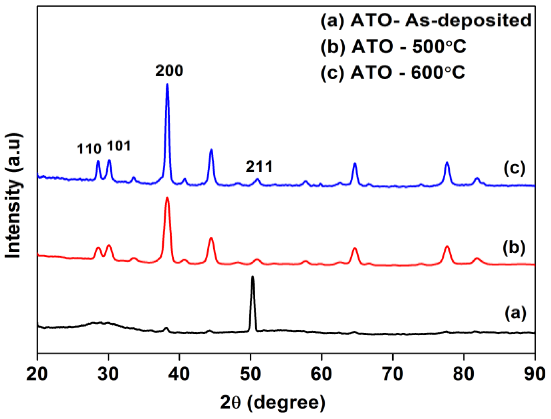
3.1. Structural Analysis

The XRD pattern of the as-deposited and annealed (at 500 °C and 600 °C) ATO films is shown in Figure 3. With an average crystallite size of 16.14 nm, the as-deposited film exhibits a broad diffraction pattern that corresponds to the plane (211). The Bragg reflection of the ATO thin-film planar lattice (200) is responsible for the observed decline in peak diffraction in the film annealed at 500 °C. The increase in crystallinity with an annealing temperature at 500 °C is represented by the significant appearance of the (200) peak. The thin film annealed at 600 °C with the predominant (200) orientation exhibits improved crystallinity and a well-resolved structure that is visible throughout the spectrum. The adsorption of NO2 gas molecules is favored by this enhanced crystallinity, which in turn enhances the sensor response. As-deposited, annealed ATO thin films at 500 °C and 600 °C exhibited an orthorhombic SnO2 structure in their diffraction pattern [17,18]. The pattern clearly shows that the (200) peak intensity rises because of annealing, which is evidence of improved crystallinity and the structural reorientation process in films. Sb3+ ions substitute Sn4+ in the tin oxide lattice in the prepared film [19,20]. The (200) peak grows substantially and the (211) peak begins to lose dominance during the post-annealing treatment at 500 °C. This pattern is maintained with an annealing temperature of 600 °C. This behavior can be described by Ostwald’s ripening effect [21]. This phenomenon indicates that in a material made up of smaller and larger crystallites, such as a crystalline solid, the smaller crystallites will tend to diffuse into the larger crystallites when they are exposed to sufficient thermal energy. The annealing temperature gives the prepared film the necessary thermal energy for this process to take place, and recrystallization begins at 500 °C.
Scherrer’s equation is used to determine the film’s structural properties. The presence of structural defects during deposition and the condensed accumulation of adatoms are responsible for the difference in crystallite size between as-deposited and annealed films. As crystallization begins and the number of defects within the film decreases, the average crystallite size increases at 500 °C. A further rise in the average crystallite size at 600 °C is attributed to densification in the film and modifications in the grain boundary, which fill up the micropores and remove stress. An improved film stability is observed by the dislocation termination seen at higher annealing temperatures. It was found that by reducing the concentration of lattice defects, it was shown that the microstrain and dislocation density decreased with increasing annealing temperature.

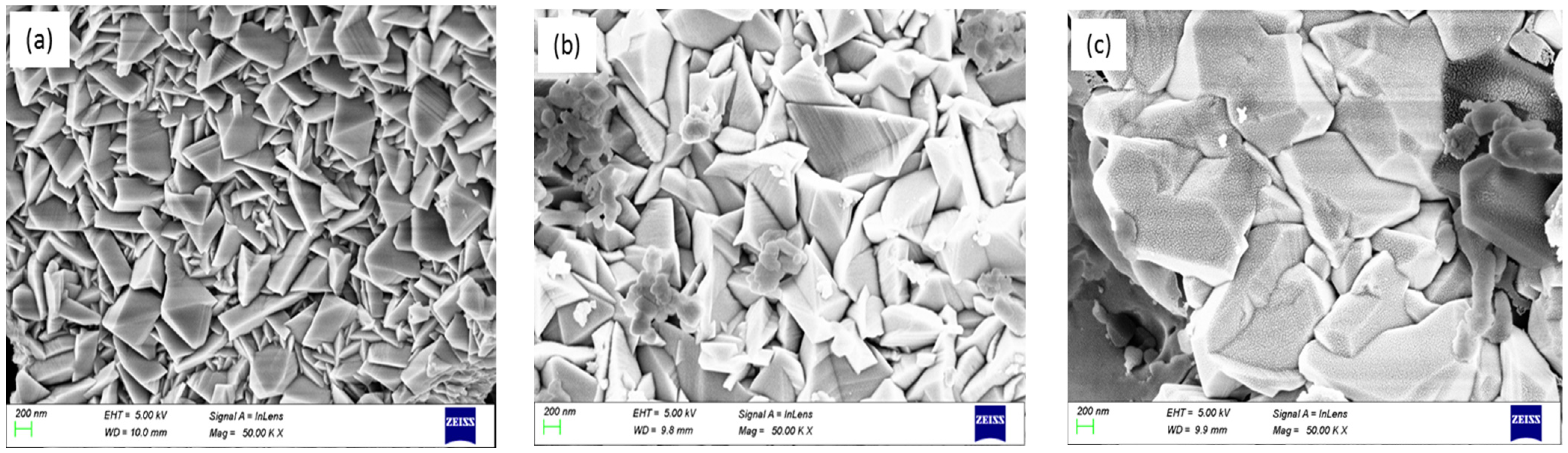
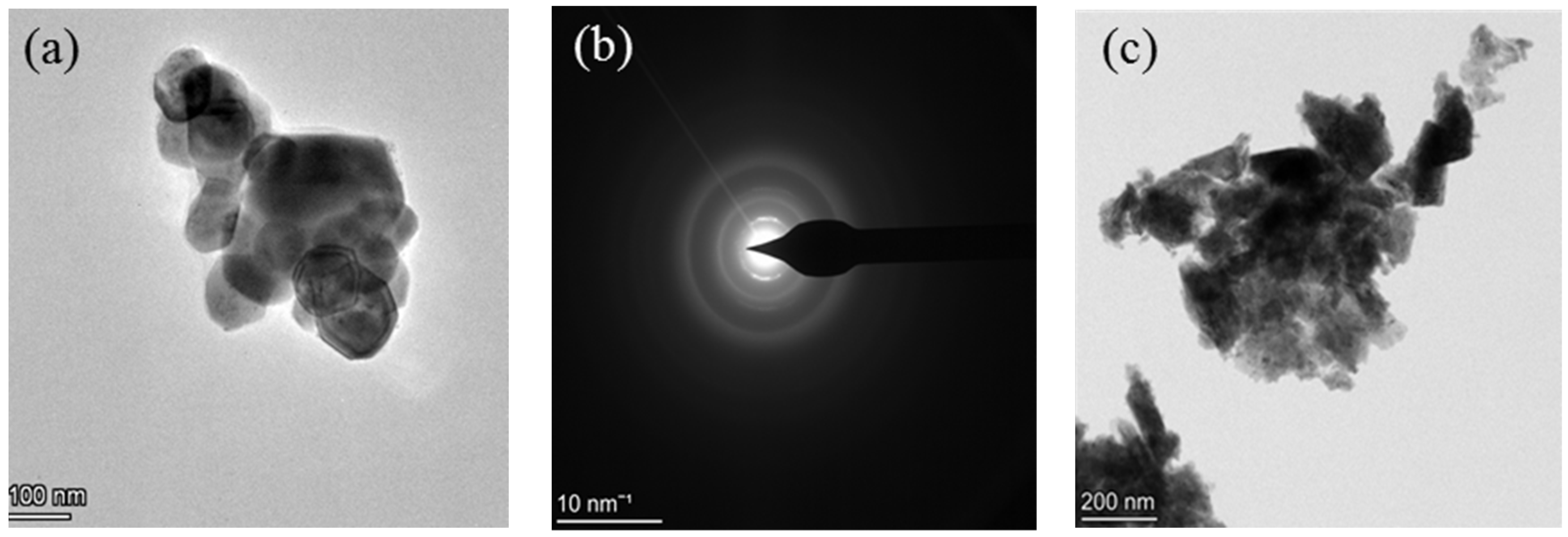
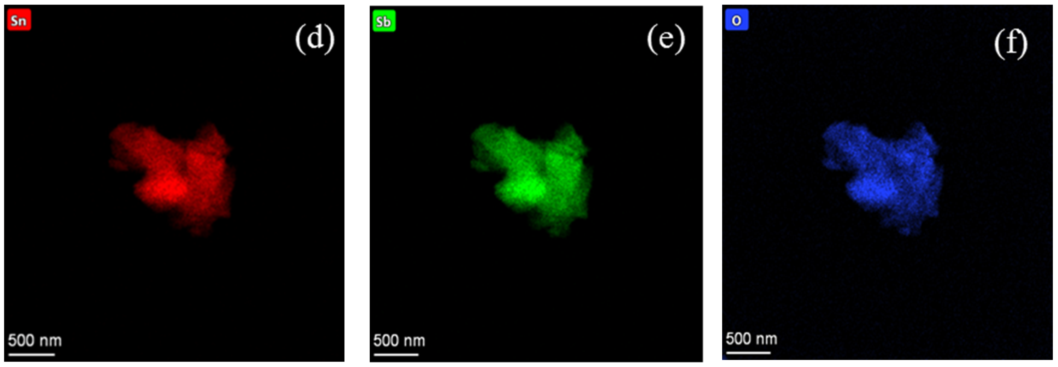
3.2. Surface Morphological Study

Using a scanning electron microscope, the microstructural characteristics of the ATO films were determined and are displayed in Figure 4. The effect of annealing on the size of grains is observed in all the images that were captured at similar magnifications. Granular-shaped ATO grains are seen in the images of SEM [22,23,24,25,26]. The boundaries of grains are distinctly visible in the as-deposited ATO thin film. Improved structural appearance without any voids, pinholes, or cracks is shown by the obtained morphology. The entire film surface is covered by agglomerated granular-shaped nano-sized surface grains. The annealing temperature has an impact on the film’s crystallographic texture. Larger grains are produced because of annealing, which lowers interfacial energy and increases the number of nucleation centers in the films. After the annealing process, ATO grains aggregate at 500 °C and 600 °C of annealing treatment, and hence, some large particles are seen [27]. However, the grain size is larger than the expected crystallite size based on XRD findings due to the aggregation of smaller crystallites. It is noticed that the SEM analysis shows high agreement with the XRD results.
Figure 5a–f shows TEM images of ATO films. Figure 5a displays an image of an as-deposited film with granular crystals. The cassiterite or tetragonal-based ATO nanostructures are inferred from the SAED and XRD patterns of the as-deposited film depicted in Figure 5b to be in good agreement. The SAED pattern from a typical area reveals crystallinity and clearly defined Scherrer’s diffraction rings that align with the ATO planes (110), (101), (200), and (211). Figure 5c shows aggregated particles of the film annealed at 600 °C. In Figure 5d–f, the nanometer-sized particles of Sn, Sb, and O are distinguished clearly. It was noticed from structural studies that with the increase in annealing temperature, the grain size also increases and is described by the Ostwald ripening effect. The TEM results show a good match with the literature [28,29].

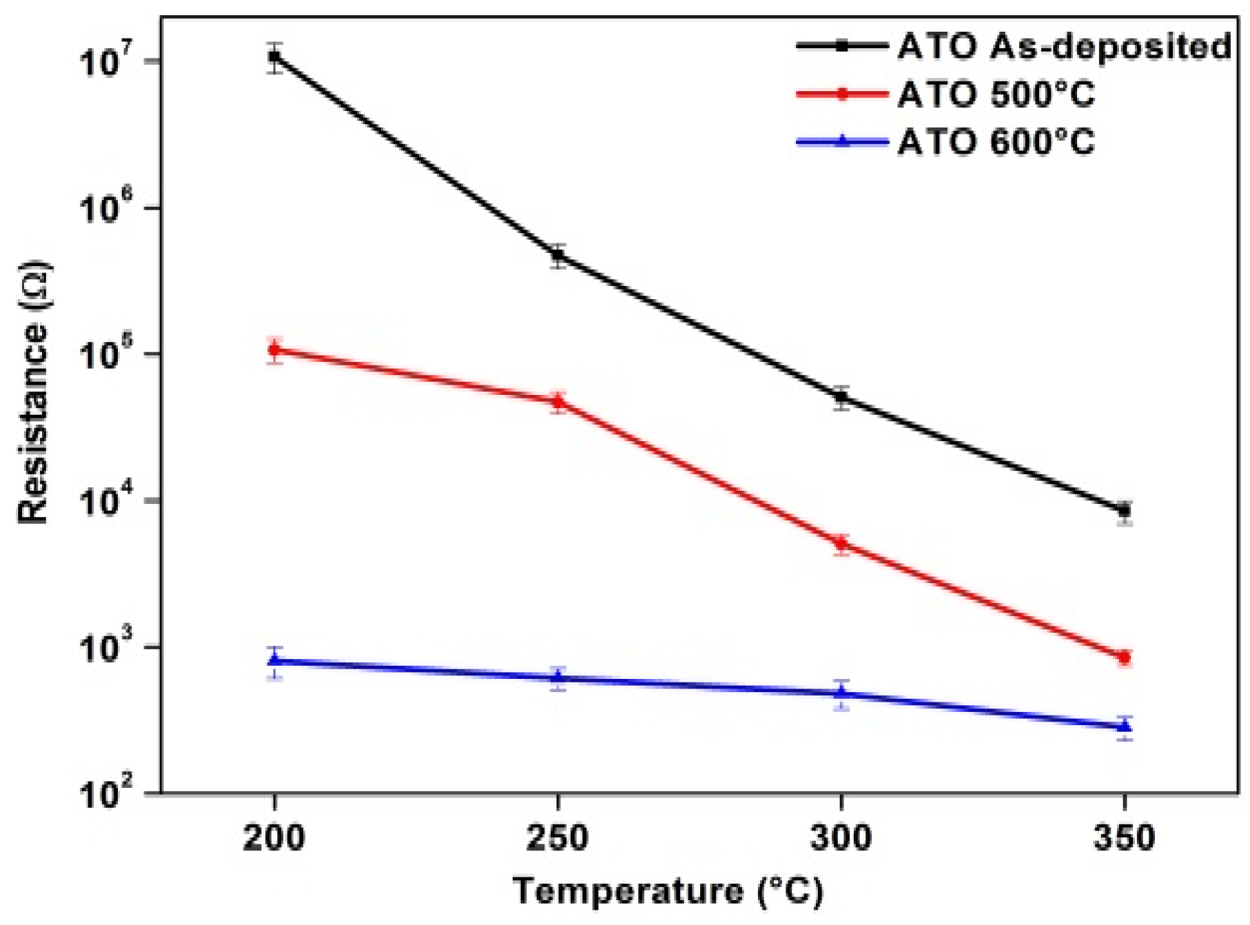
3.3. Electrical Resistance Measurement

The resistance variation of ATO thin films concerning temperature is shown in Figure 6. The film resistance was measured in steps of 50 °C at temperatures ranging from 150 °C to 350 °C. The characteristics show that the film resistance significantly decreases as the temperature rises, confirming the semiconductor behavior of ATO films [30,31,32,33,34]. At different temperatures, due to the increased surface conductivity of the annealed films, the resistance is lesser than as-deposited films. Higher annealing temperatures resulted in reduced resistivity of the produced film, as indicated by the film resistance coated on normal IDEs. Thus, at a higher annealing temperature, the response of the film is improved due to the increase in the nanoparticle’s size at the interfaces of the film surface.

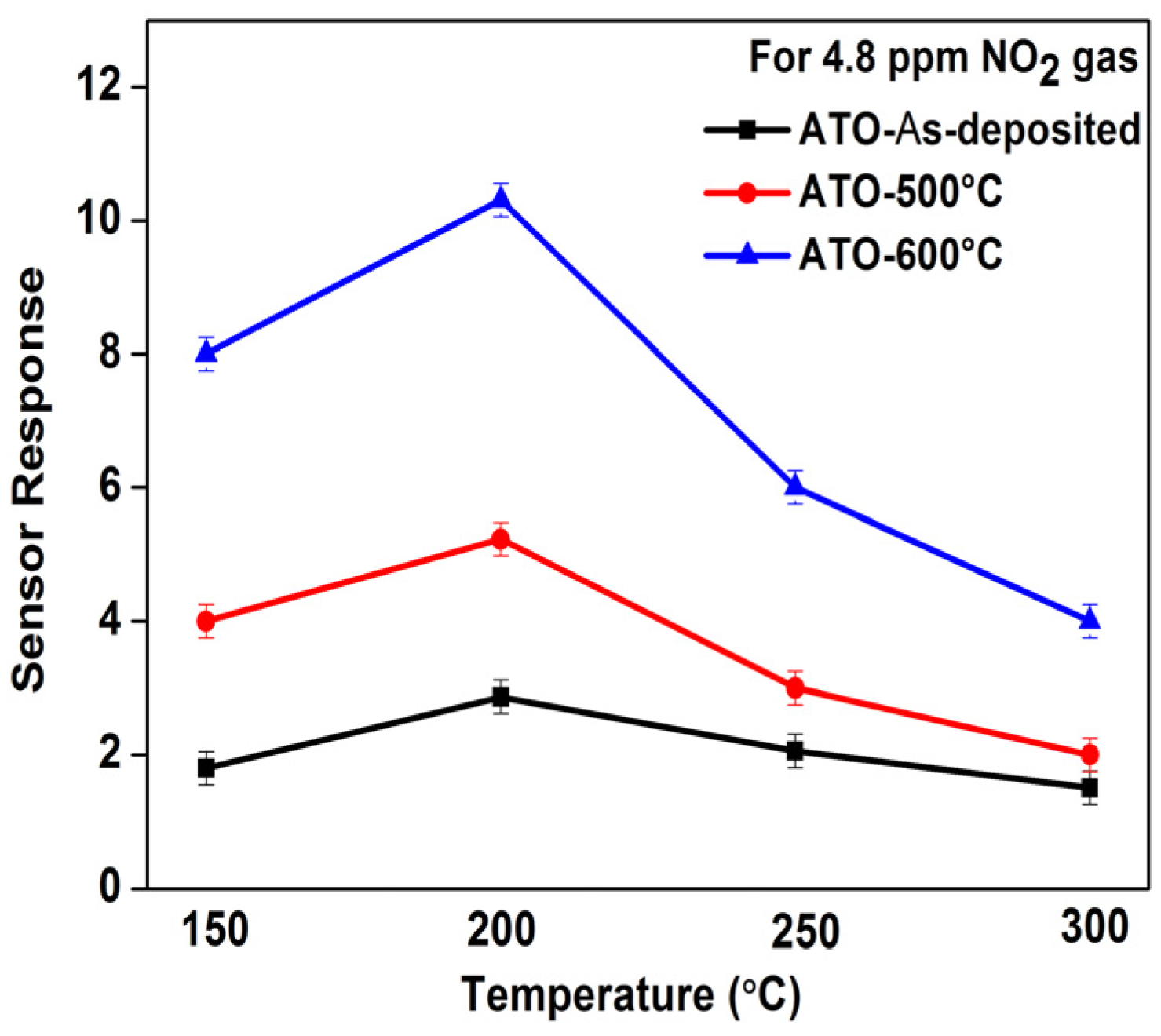
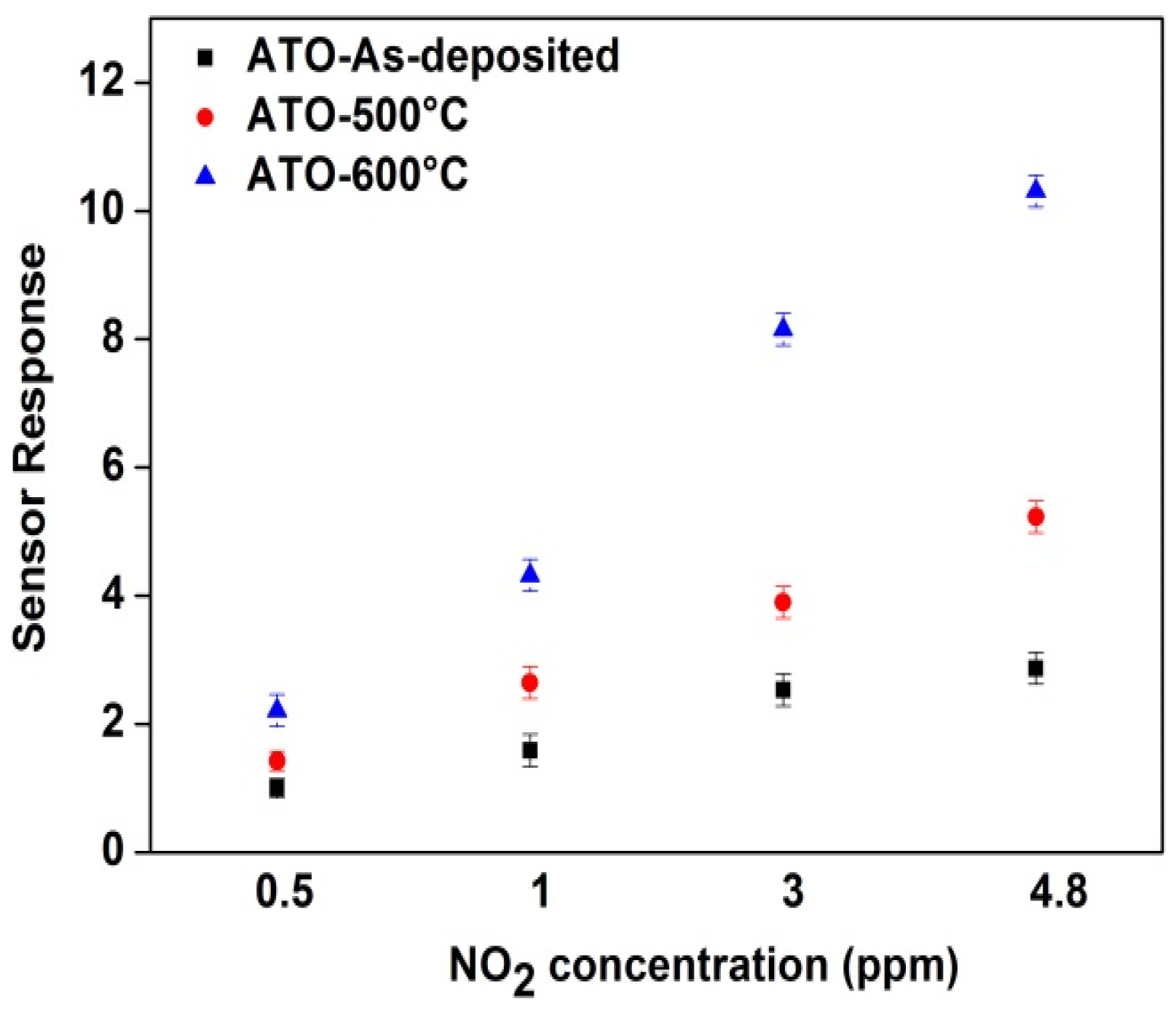
3.4. Gas Sensing Characterization of ATO Films Deposited on Normal IDEs

The analysis of the effect of annealing temperatures is carried out using a gas sensor calibration setup.
Effect of operating temperature: Initial measurements of the response of ATO films were carried out as a function of different operating temperatures with 4.8 ppm of NO2 gas to determine the optimum working temperature. The sensor response tends to increase at lower temperatures and was at its maximum at 200 °C; after this, it tends to decrease. The obtained response is due to the speed of gas molecule diffusion at higher temperatures and the speed of the chemical reaction at lower temperatures. The reaction cannot be sufficiently activated at lower and extremely higher temperatures; the sensor response is limited by NO2 desorption. The plot containing the variation in sensor response with different working temperatures is shown in Figure 7. The optimum working temperature of ATO films was found to be 200 °C.
Effect of annealing temperature: As-deposited and annealed (at 500 °C and 600 °C) thin film responses with an increase in NO2 gas at an optimum temperature of 200 °C are illustrated in Figure 8. The response trend has an error of ±0.25 for NO2 concentrations of 0.5, 1.0, 3.0, and 4.8 ppm. Because of its crystallinity, there is a noticeable variation in the response at higher annealing temperatures.

3.5. Gas Sensing Characterization of Packaged NO2 Gas Sensor

The packaged sensor consists of an ATO film annealed at 600 °C and coated on a microheater-based IDE. Investigations on the sensitivity, cross-sensitivity, and film stability of the packaged sensor are carried out using a gas sensor calibration setup.
Performance study of packaged NO2 gas sensor: For films coated on microheater-based IDEs, performance studies were conducted. Figure 9 displays the packaged sensor response of the ATO film. However, the response and recovery times of the sensor were excessively long due to the velocity of the gas inflow and outflow rate in the dynamic testing system.
(i)
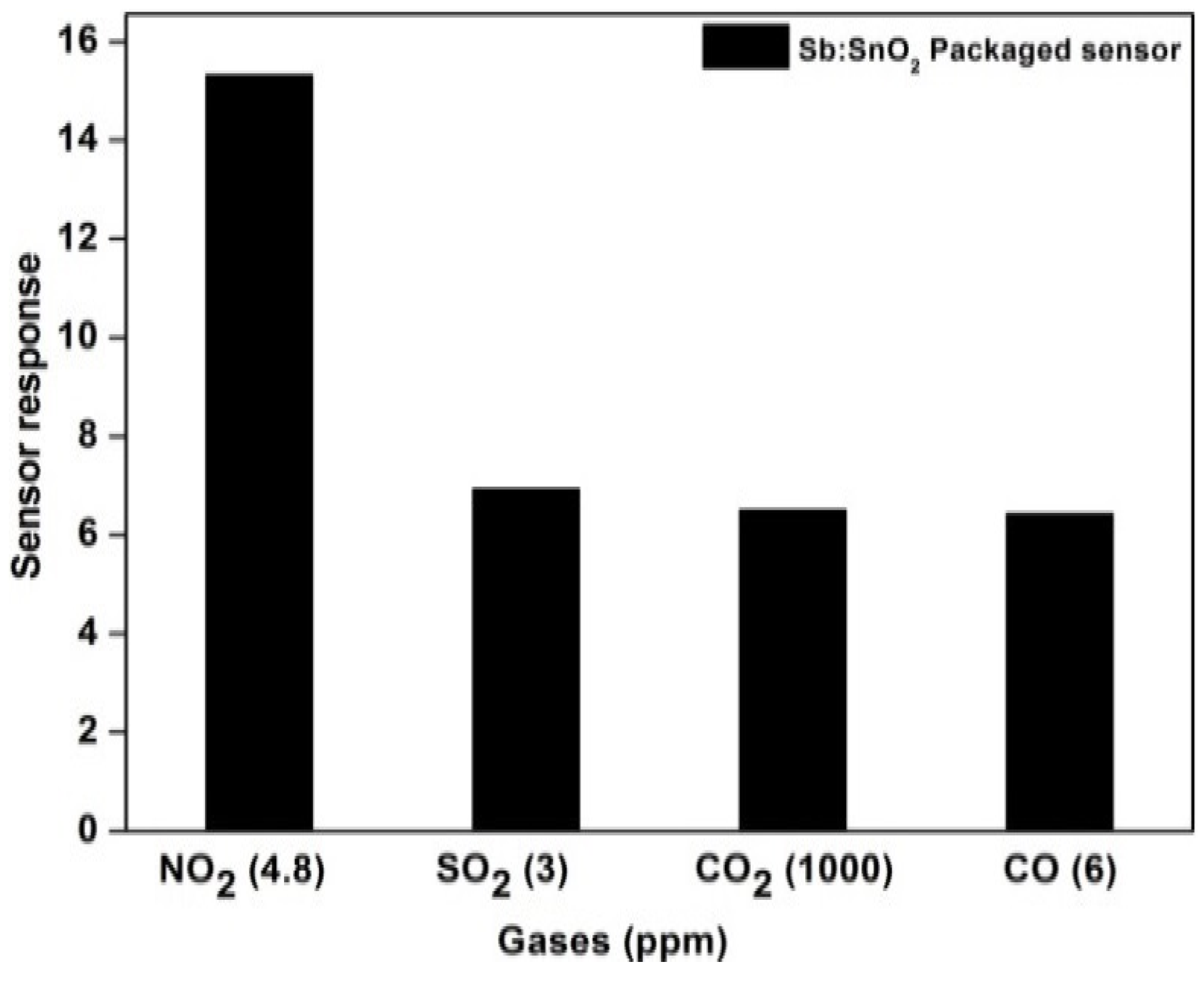
Cross-sensitivity of packaged sensor: The packaged gas sensor exhibits a response of 15.30 for NO2 gas (4.8 ppm), 6.52 for CO2 gas (1000 ppm), 6.94 for SO2 gas (3.2 ppm), and 6.44 for CO gas (4.8 ppm). The cross-sensitivity of the packaged sensor is shown in Figure 10, and it is observed that the ATO thin film exhibited good selectivity to NO2 gas.
(ii)
Stability of packaged sensor: Herein, we recorded the response to 4.8 ppm of NO2 gas at 200 °C for six months. Since the response deviation over 4 months is around 6%, the packed sensor exhibits good stability of response when the film is prepared using target nanoparticles obtained by the green chemistry method. Additionally, the sensor’s response is enhanced by the device’s packaging using IDEs with a microheater.
(iii)
Comparative studies: The responses of films coated on a die with a normal IDE and microheater-based IDE for NO2 gas were compared. The film deposited on the die with the IDE and microheater demonstrated an enhanced response to NO2 gas at various concentrations. The surface-based localized heating of the die with the IDE and microheater results in an improved response.

4. Conclusions

Using ecologically friendly green synthesis nanomaterials, ATO films were prepared by E-beam evaporation and then vacuum annealed at 500 °C and 600 °C. According to the investigations of morphological and structural properties, the prepared films are stoichiometric and have good uniformity, non-toxicity, and good adherence to the substrate. The 600 °C annealed film demonstrates an improved response at 200 °C. ATO films demonstrate higher selectivity towards NO2 among CO, CO2, SO2, and NO2 gases by cross-sensitivity tests. ATO films coated on a die with an IDE and microheater by the E-beam evaporation method in a vacuum atmosphere (10−5 mbar) and annealed at 600 °C are used in the construction of gas sensors. The gas sensing studies of the packaged sensor consisting of a die with an IDE and microheater exhibited an improved response to NO2 gas.

Supplementary Materials

The following supporting information can be downloaded at: https://www.mdpi.com/article/10.3390/micro4030025/s1, Figure S1. (a) Photograph of microheater-based IDE, (b) photograph of normal IDE, and (c) dimensions of mechanical mask. Figure S2. EDX spectrum of ATO film: (a) as-deposited, (b) annealed at 500 °C, (c) annealed at 600 °C. Table S1. Atomic and weight percentages of ATO films.

Author Contributions

C.C.: design, methodology, writing—original draft; H.M.K.: writing—review and editing, supervision, validation; C.M.A.: writing—review and editing, validation; M.B.K.: writing—review and editing, supervision, validation. All authors have read and agreed to the published version of the manuscript.

Funding

This research received no external funding.

Institutional Review Board Statement

Not Applicable.

Informed Consent Statement

Exclude this statement.

Data Availability Statement

We have provided the Supplementary Materials Section with all the data availability.

Acknowledgments

The authors are thankful to INUP at CeNSE, IISc, Bangalore, for providing the gas sensing testing facility, and are also thankful to the management of the Siddaganga Institute of Technology for providing the research facility and the Vision Group of Science and Technology (VGST), Government of Karnataka, for providing funds under the CISEE program (No. VGST/P-10/CISEE-2010-11/2011-2/1133) to procure the Vacuum box coater (BC-100) from Hind High Vacuum Co. (P) Ltd., Bangalore.

Conflicts of Interest

The authors declare that they have no known competing financial interests or personal relationships that could have appeared to influence the work reported in this paper.

References

  1. Jeong, H.S.; Park, M.J.; Kwon, S.H.; Joo, H.J.; Kwon, H.I. Highly sensitive and selective room-temperature NO2 gas- sensing characteristics of SnOX-based p-type thin-film transistor. Sens. Actuators B Chem. 2019, 288, 625–633. [Google Scholar] [CrossRef]
  2. Sharma, A.; Tomar, M.; Gupta, V. Enhanced response characteristics of SnO2 thin film based NO2 gas sensor integrated with nanoscaled metal oxide clusters. Sens. Actuators B Chem. 2013, 181, 735–742. [Google Scholar] [CrossRef]
  3. Gomaa, M.M.; Sayed, M.H.; Patil, V.L.; Boshta, M.; Patil, P.S. Gas sensing performance of sprayed NiO thin films toward NO2 gas. J. Alloys Compd. 2021, 885, 160908. [Google Scholar] [CrossRef]
  4. Boomashri, M.; Perumal, P.; Gunavathy, K.V.; Alkallas, F.H.; Trabelsi, A.B.G.; Shkir, M.; AlFaify, S. Detection of ammonia gas at room temperature through Sb doped SnO2 thin films: Improvement in sensing performance of SnO2. Ceram. Int. 2023, 49, 10096–10106. [Google Scholar] [CrossRef]
  5. Patil, V.L.; Vanalakar, S.A.; Patil, P.S.; Kim, J.H. Fabrication of nanostructured ZnO thin films based NO2 gas sensor via SILAR technique. Sens. Actuators B Chem. 2017, 239, 1185–1193. [Google Scholar] [CrossRef]
  6. Tyagi, S.; Chaudhary, M.; Ambedkar, A.K.; Sharma, K.; Gautam, Y.K.; Singh, B.P. Metal oxide nanomaterial-based sensors for monitoring environmental NO 2 and its impact on the plant ecosystem: A review. Sens. Diagn. 2022, 1, 106–129. [Google Scholar] [CrossRef]
  7. Kim, T.H.; Hasani, A.; Van Quyet, L.; Kim, Y.; Park, S.Y.; Lee, M.G.; Sohn, W.; Nguyen, T.P.; Choi, K.S.; Kim, S.Y.; et al. NO2 sensing properties of porous Au-incorporated tungsten oxide thin films prepared by solution process. Sens. Actuators B Chem. 2019, 286, 512–520. [Google Scholar] [CrossRef]
  8. Liu, H.; Wan, J.; Fu, Q.; Li, M.; Luo, W.; Zheng, Z.; Cao, H.; Hu, Y.; Zhou, D. Tin oxide films for nitrogen dioxide gas detection at low temperatures. Sens. Actuators B Chem. 2013, 177, 460–466. [Google Scholar] [CrossRef]
  9. Kulkarni, M.B.; Upadhyaya, K.; Ayachit, N.H.; Iyer, N. Quantum Dot–Polymer Composites in Light-Emitting Diode Applications. In Quantum Dots and Polymer Nanocomposites; CRC Press: Boca Raton, FL, USA, 2022; pp. 259–279. [Google Scholar]
  10. Ingole, S.M.; Navale, S.; Navale, Y.; Bandgar, D.; Stadler, F.; Mane, R.; Ramgir, N.; Gupta, S.; Aswal, D.; Patil, V. Nanostructured tin oxide films: Physical synthesis, characterization, and gas sensing properties. J. Colloid Interface Sci. 2017, 493, 162–170. [Google Scholar] [CrossRef]
  11. Jaiswal, J.; Singh, P.; Chandra, R. Low-temperature highly selective and sensitive NO2 gas sensors using CdTe-functionalized ZnO filled porous Si hybrid hierarchical nanostructured thin films. Sens. Actuators B Chem. 2021, 327, 128862. [Google Scholar] [CrossRef]
  12. Sundar, S.; Chakravarty, J. Antimony toxicity. Int. J. Environ. Res. Public Health 2010, 7, 4267–4277. [Google Scholar] [CrossRef] [PubMed]
  13. Siciliano, T.; Tepore, A.; Micocci, G.; Serra, A.; Manno, D.; Filippo, E. WO3 gas sensors prepared by thermal oxidization of tungsten. Sens. Actuators B Chem. 2008, 133, 321–326. [Google Scholar] [CrossRef]
  14. Ani, A.; Poornesh, P.; Antony, A.; Nagaraja, K.K.; Rao, A.; Hegde, G.; Kolesnikov, E.; Shchetinin, I.V.; Kulkarni, S.D.; Petwal, V.C.; et al. An 8 mev electron beam modified in: Zno thin films for co gas sensing towards low concentration. Nanomaterials 2021, 11, 3151. [Google Scholar] [CrossRef] [PubMed]
  15. Mane, A.A.; Moholkar, A.V. Palladium (Pd) sensitized molybdenum trioxide (MoO3) nanobelts for nitrogen dioxide (NO2) gas detection. Solid-State Electron. 2018, 139, 21–30. [Google Scholar] [CrossRef]
  16. Chaitra, C.; Kalpana, H.M.; Ananda, C.M.; Lalithamba, H.S. Green synthesis of tin oxide based nanoparticles using Terminalia bellirica seed extract: Impact of operating temperature and antimony dopant on sensitivity for carbon dioxide gas sensing application. Mater. Technol. 2022, 37, 2339–2346. [Google Scholar] [CrossRef]
  17. Kim, J.; Murdoch, B.J.; Partridge, J.G.; Xing, K.; Qi, D.; Lipton-Duffin, J.; McConville, C.F.; van Embden, J.; Della Gaspera, E. Ultrasonic Spray Pyrolysis of Antimony-Doped Tin Oxide Transparent Conductive Coatings. Adv. Mater. Interfaces 2020, 7, 2000655. [Google Scholar] [CrossRef]
  18. Kulkarni, M.B.; Ayachit, N.H. Energy conversion and storage devices. In Green Nanomaterials in Energy Conversion and Storage Applications; Apple Academic Press: Palm Bay, FL, USA, 2024; pp. 75–93. [Google Scholar]
  19. Krishnakumar, T.; Jayaprakash, R.; Pinna, N.; Phani, A.; Passacantando, M.; Santucci, S. Structural, optical and electrical characterization of antimony-substituted tin oxide nanoparticles. J. Phys. Chem. Solids 2009, 70, 993–999. [Google Scholar] [CrossRef]
  20. Zheng, H.; Li, L.; Sun, Z.; Yu, S.; Luo, W. Preferential orientation, microstructure and functional properties of SnO2:Sb thin film: The effects of post-growth annealing. Appl. Surf. Sci. 2016, 362, 230–236. [Google Scholar] [CrossRef]
  21. Kulkarni, M.B.; Vyas, R. A role of integrated microheaters in a microfluidics based point-of-care-testing and beyond for healthcare applications. Appl. Mater. Today 2024, 38, 102225. [Google Scholar] [CrossRef]
  22. Velmurugan, K.; Kulkarni, M.B.; Gupta, I.; Das, R.; Goel, S.; Nirmal, J. Role of microfluidics in drug delivery. In Microfluidics and Multi Organs on Chip; Springer: Singapore, 2022; pp. 107–133. [Google Scholar]
  23. Xiong, Y.; Lin, Y.; Wang, X.; Zhao, Y.; Tian, J. Defect engineering on SnO2 nanomaterials for enhanced gas sensing performances. Adv. Powder Mater. 2022, 1, 100033. [Google Scholar] [CrossRef]
  24. Saeedabad, S.H.; Selopal, G.S.; Rozati, S.M.; Tavakoli, Y.; Sberveglieri, G. From Transparent Conducting Material to Gas-Sensing Application of SnO2:Sb Thin Films. J. Electron. Mater. 2018, 47, 5165–5173. [Google Scholar] [CrossRef]
  25. Babar, A.R.; Shinde, S.S.; Moholkar, A.V.; Bhosale, C.H.; Kim, J.H.; Rajpure, K.Y. Structural and optoelectronic properties of antimony incorporated tin oxide thin films. J. Alloys Compd. 2010, 505, 416–422. [Google Scholar] [CrossRef]
  26. Afrouzmehr, M.; Yasrebi, N.; Sheikhi, M.H. Fabrication and characterization of Ag-Decorated indium–tin-oxide nanoparticle based ethanol sensors using an enhanced electrophoretic method. Ceram. Int. 2021, 47, 30504–30513. [Google Scholar] [CrossRef]
  27. Chen, F.; Li, N.; Shen, Q.; Wang, C.; Zhang, L. Fabrication of transparent conducting ATO films using the ATO sintered targets by pulsed laser deposition. Sol. Energy Mater. Sol. Cells 2012, 105, 153–158. [Google Scholar] [CrossRef]
  28. Peters, K.; Zeller, P.; Stefanic, G.; Skoromets, V.; Němec, H.; Kužel, P.; Fattakhova-Rohlfing, D. Water-Dispersible Small Monodisperse Electrically Conducting Antimony Doped Tin Oxide Nanoparticles. Chem. Mater. 2015, 27, 1090–1099. [Google Scholar] [CrossRef]
  29. Eom, N.S.A.; Cho, H.B.; Lim, H.R.; Kim, B.S.; Choa, Y.H. Facile tilted sputtering process (TSP) for enhanced H2S gas response over selectively loading Pt nanoparticles on SnO2 thin films. Sens. Actuators B Chem. 2019, 300, 127009. [Google Scholar] [CrossRef]
  30. Rudraswamy, S.B.; Bhat, N. Optimization of RF sputtered Ag-Doped BaTiO3-CuO mixed oxide thin film as carbon dioxide sensor for environmental pollution monitoring application. IEEE Sens. J. 2016, 16, 5145–5151. [Google Scholar] [CrossRef]
  31. Li, H.; Zhao, J.; Wu, T.; Fu, Z.; Zhang, W.; Lian, Z.; Cai, S.; Yang, R. Dual ligand-induced photoelectrochemical sensing by integrating Pt/MoS2 heterostructure and Au polyhedra for sensitive detection of SARS-CoV-2. Sens. Actuators B Chem. 2023, 376, 132970. [Google Scholar] [CrossRef]
  32. Thomas, A.; Thirumalaisamy, L.; Madanagurusamy, S.; Sivaperuman, K. Incompatibility of pure SnO2 thin films for room-temperature gas sensing application. ACS Omega 2023, 8, 32848–32854. [Google Scholar] [CrossRef]
  33. Zhou, L.; Li, Z.; Chang, X.; Liu, X.; Hu, Y.; Li, M.; Xu, P.; Pinna, N.; Zhang, J. PdRh-sensitized iron oxide ultrathin film sensors and mechanistic investigation by operando TEM and DFT calculation. Small 2023, 19, 2301485. [Google Scholar] [CrossRef]
  34. Pan, H.; Zhou, L.; Zheng, W.; Liu, X.; Zhang, J.; Pinna, N. Atomic layer deposition to heterostructures for application in gas sensors. Int. J. Extrem. Manuf. 2023, 5, 022008. [Google Scholar] [CrossRef]
Figure 1. (a) Packaged design of the sensor. (b) Photograph of packaged NO2 gas sensor.
Micro 04 00025 g001
Figure 2. Schematic diagram of the sensor calibration system.
Micro 04 00025 g002
Figure 3. XRD results of prepared ATO films.
Micro 04 00025 g003
Figure 4. SEM images of ATO films: (a) as-deposited; (b) annealed at 500 °C; (c) annealed at 600 °C.
Micro 04 00025 g004
Figure 5. TEM images: (a) nanoparticles; (b) SAED pattern of the as-deposited film; (c) nanoparticles of 600 °C annealed film; (df) images of elements Sn, Sb, and O in as-deposited film.
Micro 04 00025 g005aMicro 04 00025 g005b
Figure 6. Plot of film resistance versus temperature.
Micro 04 00025 g006
Figure 7. Plot of variation in ATO films’ response with temperature.
Micro 04 00025 g007
Figure 8. Plot of sensor response of ATO films with NO2 concentration.
Micro 04 00025 g008
Figure 9. Packaged NO2 gas sensor response.
Micro 04 00025 g009
Figure 10. Cross-sensitivity of the packaged sensor.
Micro 04 00025 g010
Table 1. Summary of NO2 gas sensor performance parameters developed by various researchers.
InvestigatorDeposition MethodThin-Film
Material
Operating TemperatureResponseResponse/Recovery TimeReference
Siciliano et al.
(2008)
Thermal EvaporationWO3250 °C4-[13]
Luís F. da Silva
et al. (2015)
E-beam evaporationSrTi0.85Fe00.15O3260 °C415 s/35 s[14]
Mane et al.
(2017)
Chemical Spray PyrolysisPd:MoO3200 °C4.511 s/76 s[15]
This workE-beam EvaporationSb:SnO2200 °C16.20285/510 s-
Table 2. Optimized parameters for deposition of ATO films.
Process ParametersValues
Base pressure2 × 10−3 mbar
Working pressure5 × 10−5 mbar
Target-to-substrate distance13 cm
Substrate temperature27 °C
Accelerating voltage5 KV
Beam current20 mA
Rate of deposition0.9 Å/s
Film thickness~250 nm
Disclaimer/Publisher’s Note: The statements, opinions and data contained in all publications are solely those of the individual author(s) and contributor(s) and not of MDPI and/or the editor(s). MDPI and/or the editor(s) disclaim responsibility for any injury to people or property resulting from any ideas, methods, instructions or products referred to in the content.

