1. Introduction
Power semiconductors impact every energy conversion process, from generation to transmission, distribution and utilization, and tiny incremental gains in efficiency can easily translate into remarkable savings. N. Mohan, T.M. Undeland and W.P. Robbins, editors of a textbook on Power Electronics [
1], give the following definition of power electronics that probably captures its mission most effectively: “In broad terms, the task of power electronics is to process and control the flow of electric energy by supplying voltages and currents in a form that is optimally suited for user loads”.
This statement attests to the key role of power electronics in reducing power losses. Now, with the growth in and adoption of EVs, there is a focus on the electric vehicle’s inverter to extend its driving range for a given battery pack. This is one example of the role of power electronics in everyday life providing incentives to develop more efficient semiconductor devices.
The COVID-19 pandemic has accelerated the decline in traditional internal combustion engine (ICE) vehicles and the corresponding emergence of electrified platforms. Despite plummeting car sales with an estimated CAGR (compound average growth rate) of −8% between 2018 and 2022, the semiconductor content in cars has increased, leading to a robust +27% growth in automotive semiconductors in the same time frame according to Strategy Analytics. If the number of silicon chips per car grew by 50% from 2002 to 2017, in the last four years to 2021, it has doubled.
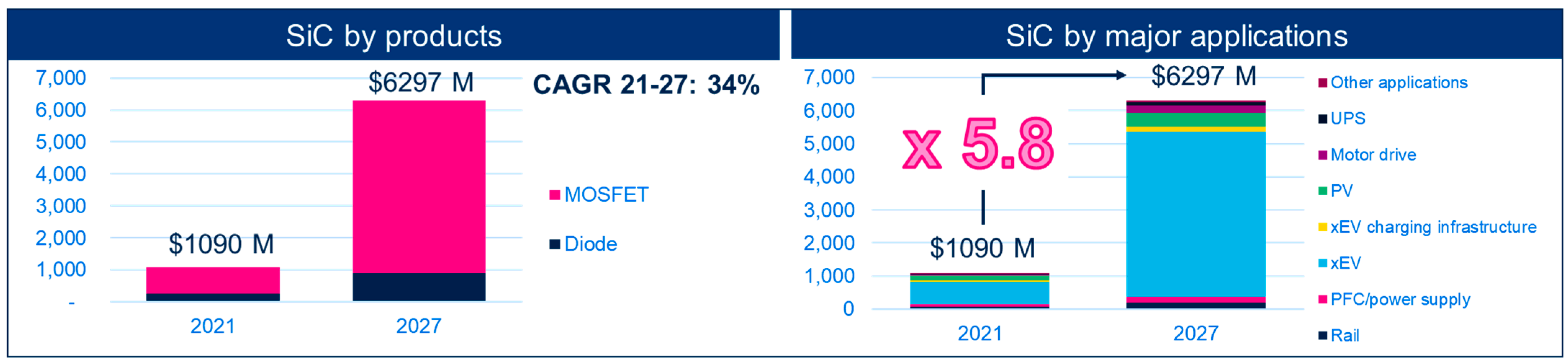
The growth of silicon carbide (SiC) has been the most impressive; according to Yole, the total market for SiC will peak at USD 6.3B in 2027 up from USD 1B in 2021 (34% CAGR), driven, to a very large extent, by car electrification.
Until now, silicon has dominated the semiconductor market, and it is a mature technology where further improvements in performance will most likely be incremental. Silicon carbide presents a big opportunity today.
2. Power Semiconductor Technologies
Figure 1 depicts, in a power–frequency diagram, today’s main power technologies [
2]. Wide bandgap (WBG, SiC and GaN) materials have been introduced because their smaller on-resistance and higher frequency operation drastically reduce total losses and increase efficiency. Except for a small overlap above 650 V, gallium nitride (GaN) is used in the range from 100 V to 900 V, while SiC supports even higher voltage applications, well above 650 V and even beyond 2000 V. GaN HEMTs (High Electron Mobility Transistors), unlike SiC, exhibit a lateral structure which limits their voltage capability to below 900 V. On the other hand, as the picture shows, GaN can operate at higher frequencies (close to the MHz range) than those covered by SiC. This feature depends on their smaller specific on-resistance, which translates into smaller chip sizes with smaller capacitances, and superior electron mobility (see
Figure 2). For these reasons, GaN HEMTs are very suitable for DC-DC converters and OBCs (on-board chargers), where a high frequency implies smaller passive components. In any case, GaN’s higher power density and poor thermal conductivity vs. SiC pose some challenges for packaging and heatsinking.
Among more traditional silicon technologies, the IGBT (Insulated Gate Bipolar Transistor) has been used extensively in motor drives at different power levels, while super-junction MOSFETs (Metal Oxide Semiconductor Field-Effect Transistors) lend themselves to address a large variety of power supplies and converters, due to their inherently higher frequency capability. With these overlaps, in high-power inverters, for instance, SiC MOSFETs can replace IGBTs to deliver the higher performance that would be needed in an electric vehicle (EV) traction inverter and in fast chargers. SiC MOSFETs can also replace silicon high-voltage MOSFETs for improved efficiency and enable new circuit topologies.
3. SiC Physical Structure and Electrical Properties
SiC is not native to our planet. Historically, fragments of this material (called also “carborundum”), the second hardest natural mineral after diamond, were discovered in 1893 by the French chemist Henri Moissan in a crater at Canyon Diablo, Arizona. They were created by the impact of a meteorite almost 50,000 years ago that evidently created the favorable extreme conditions necessary to form SiC from its two basic elements. Today, the extra-terrestrial origin of SiC is proven by its carbon isotopic composition, defined as the ratio of 12C isotope concentration to that of 13C; this value is in fact about 64 which turns out to be lower than what was measured in material of terrestrial origin. Scientists artificially synthesized SiC just two years after its discovery.
The history of SiC products overlaps with STMicroelectronics’s development efforts dating back to the end of the 1990s. All started, as usual, as an advanced investigation into its promising characteristics that involved academic and industrial research carried out on small wafer sizes (1”). Thanks to the initial rudimentary epitaxial reactor, the first demonstrations of Schottky diodes were produced in 2004 using 3” wafers. After a couple of years, production of first-generation diodes was started. The first positive results encouraged a team of physicists and the Company’s R&D team to prove the feasibility of a planar vertical power MOSFET in 2008. Such a milestone was instrumental in designing the first generation of 1,200 V MOSFETs for industrial use, with mass production started in 2014 on 4” wafers. In the meantime, Schottky diode technology evolved to the third generation. Successive switchover to 6” and introduction of automotive-grade MOSFETs have greatly contributed to a quick production ramp-up. As of today, more than 250 million chips have been shipped for EV applications, allowing the company to go through a very fast learning curve. Although technology iterations are being introduced, 8” prototypes have also been successfully debugged.
SiC is an IV-IV wide bandgap (WBG) compound with a rigid 50% Si, 50% C stoichiometry that we have learned to use to fabricate power devices and opto electronics. Its physical properties—large bandgap, high breakdown field, high saturation drift velocity and high thermal conductivity—make it ideal for applications operating at high temperatures, high intensities of radiation, high voltages or high power dissipations. Due to the low electro-thermal conductivity of silicon devices, large amounts of energy are dissipated during conversion steps of AC-DC-AC. With the output capacitance being low, it is appropriate to use SiC devices in high voltage applications. Thus, the sizing requirement of other magnetizing parts like transformers, chokes, inductors, etc., is also eliminated or reduced. Thermal performance improvement is another major factor attracting designers’ interest. Liquid cooling system’s sizing and cost are crucial in an EV; together with batteries, they in fact account for the largest costs of any EV. A more detailed study on the temperature characteristics with respect to bandgap, carrier mobility, saturation velocity, thermal conductivity and converter efficiencies can be found in [
3].
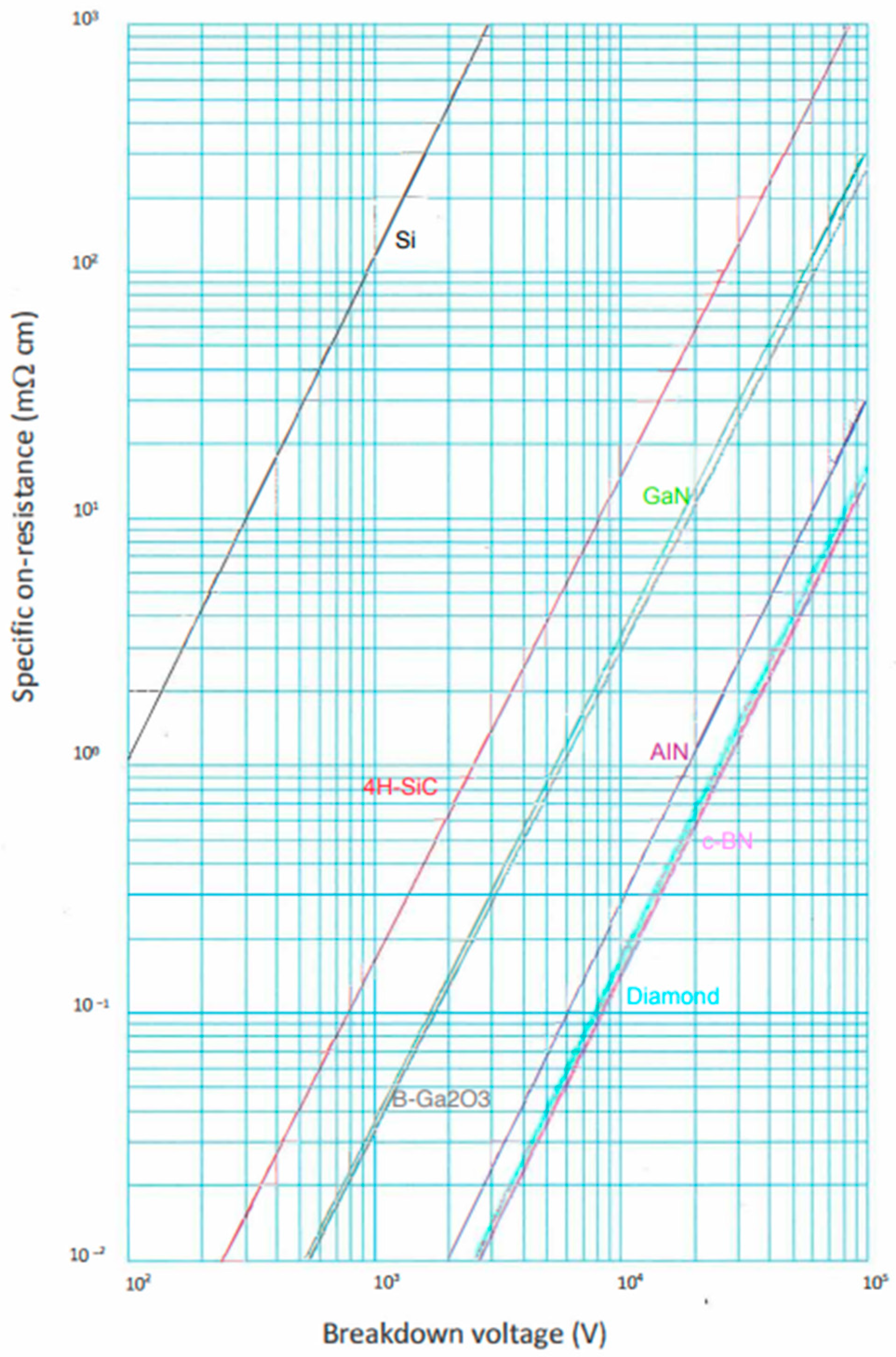
The bar diagrams in
Figure 2 show SiC’s main physical and thermal parameters compared to both silicon and gallium nitride, the other key WBG members.
Figure 2b shows the structure of a planar vertical SiC MOSFET which is very similar to its silicon counterpart.
One figure-of-merit for power devices can be expressed as εμEB3 (Baliga figure-of-merit, BFOM), where ε is the dielectric constant, μ is the mobility and EB is the breakdown or critical field. The figure-of-merit of the 4H-SiC polytype (see below) is 560 times greater than silicon (240 times for the 6H-SiC polytype), which indicates the high potential of SiC for power device applications. The BFOM assumes that power losses are solely due to the power dissipation in the on-state produced by current flow through the on-resistance of the power MOSFET. In other words, the BFOM applies to systems operating at lower frequencies where conduction losses are dominant.
In high-frequency systems, switching losses are more significant. Their higher values result from the charging and discharging of the input capacitance of the MOSFET [
4].
SiC material can be synthesized in different variants called polytypes; “polytypism” is akin to polymorphism, which refers to the possibility of an element or compound crystallizing in a range of structures, while polytypes differ by virtue of the stacking sequence of atomic layers along a given crystalline direction without change in the chemical composition. For SiC material, the basic block is a tetrahedron with a C atom at the center surrounded by four Si atoms. Both Si and C in SiC have four sp3 hybridized valence electron orbitals, which form very strong Si-C covalent bonds with a dissociation energy of 1.3 eV. The dissociation energy (DE) of the Si-C bond, to a first approximation, defines the electrical properties of this material. Indeed, as the DE increases, more energy is required to ionize an atom and generate an electron–hole (e–h) pair.
Different polytypes have widely ranging physical properties which depend on the crystal structure, specifically on their hexagonality. This variation significantly influences all electrical properties of SiC polytypes, i.e., the energy gap, electron affinity, ionization energies of dopant species, mobilities, impact ionization, etc. As opposed to crystal growth, device processing parameters (annealing temperatures, oxidation, etching rates, etc.) usually do not depend on the SiC polytype, but fabricated devices made of different polytypes exhibit different characteristics. In other words, SiC is a common name for a set of materials structurally and electrically different.
The polytype 3C-SiC, for instance, has the highest electron mobility and saturation velocity because of reduced phonon scattering resulting from the higher symmetry. We recall that in quantum mechanics, a phonon is a description of a collective vibrational mode of atoms in the crystal lattice. We can visualize the atoms as being connected by minuscule springs, so by virtue of their thermal energy, the lattice vibrates, generating mechanical waves that make heat and sound propagate through the material.
The band gaps differ widely among the polytypes, ranging from 2.36 eV for 3C-SiC to 3.08 eV in 6H SiC. Among the SiC polytypes, 6H is the most easily prepared and most studied, while the 4H polytype has attracted more attention for its superior electronic properties, especially in power electronics. 4H-SiC consists of an equal number of cubic and hexagonal bonds with a stacking sequence of ABCB. 6H-SiC is composed of two-thirds cubic bonds and one-third hexagonal bonds with a stacking sequence of ABCACB. The overall symmetry is hexagonal for both polytypes, despite the cubic bonds which are present in each [
5,
6].
Table 1 summarizes the main differences between 4H- and 6H-SiC polytypes. Adding more H atoms to move from 4H- to 6H-SiC results in negative effects such as a higher intrinsic carrier density, leading to increased leakage levels and lower electron mobility to the detriment of on-resistance and current density.
Any unipolar power device, like a MOSFET, has an incorporated drift region to support the applied reverse voltage. We can derive (see Equation (1)) the features of an ideal drift region as a function of the doping concentration and thickness by assuming an abrupt junction with high doping on one side while the other side exhibits low doping and a uniform profile.
The specific on-resistance (on-resistance times chip area) can be expressed as
Equation (1) can be used to draw specific on-resistance curves that become lines in a log–log diagram, as
Figure 3 shows; the denominator equals the BFOM shown before.
Figure 3 compares a range of materials, including GaN oxide, β-GaN and others belonging to the ultra-wide bandgap family such as aluminum nitride, boron nitride and diamond. While silicon carbide exhibits a superior thermal performance with respect to GaN, the other materials are still in the realm of advanced and academic research. Diamond is by far the most promising among the materials with an BFOM of 27,000 with respect to silicon.
Both n- and p-type control across a wide doping range is relatively easy in SiC; this makes SiC unique among wide bandgap semiconductors. Furthermore, the ability of SiC to form silicon dioxide (SiO2) as a native oxide is useful and can be exploited for device fabrication.
4. Growth of Bulk SiC
Bulk crystal growth is the principal process for producing monocrystalline wafers, the base material for device fabrication. The latest progress in SiC device development is based on the availability of relatively large SiC wafers (6” today and 8” in the future) of adequate quality. As of today, the standard technique for SiC bulk growth is seeded sublimation, referred to as the modified Lely method. Sublimation is the direct phase transition from solid to gas.
SiC sublimes at very high temperatures above 1800–2000 °C and this represents the key step.
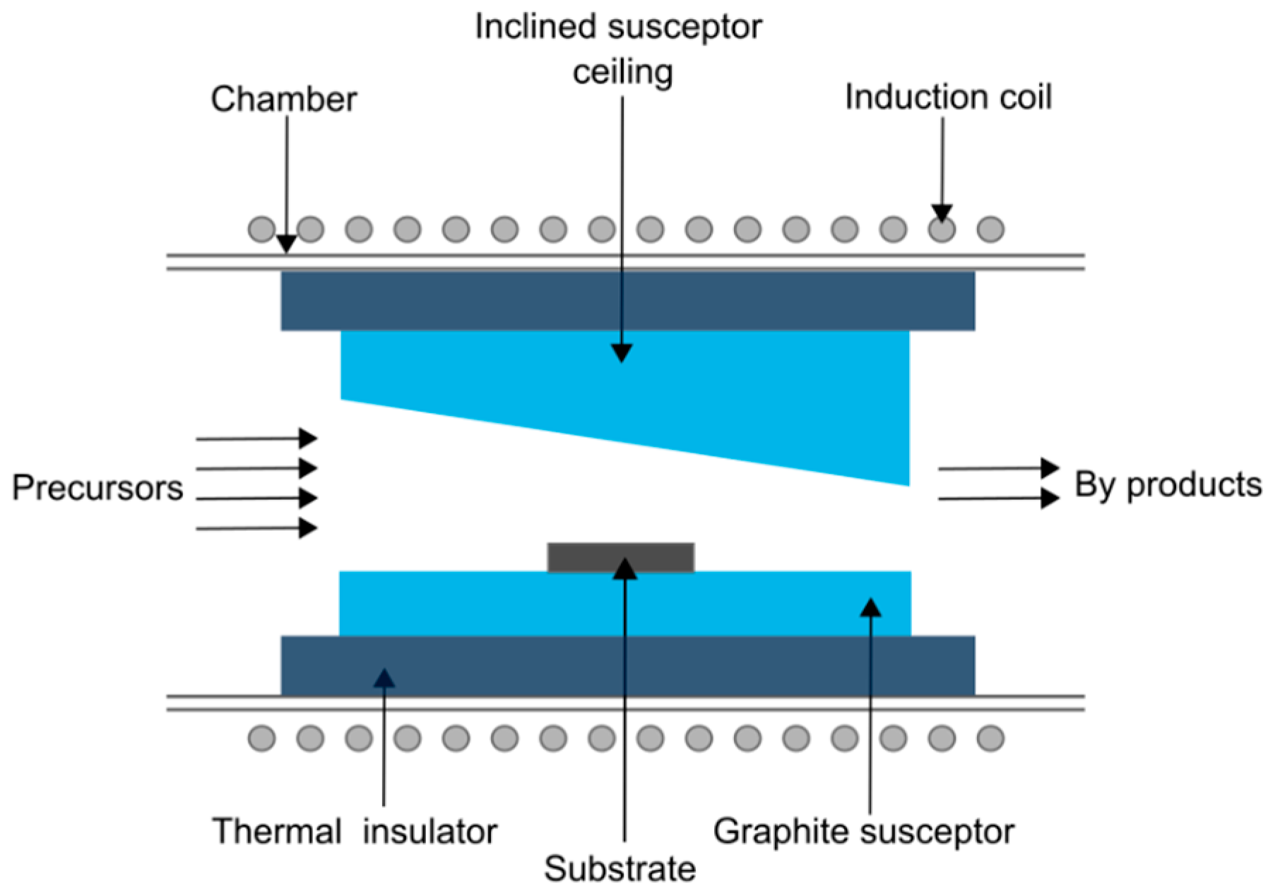
The method to grow single crystalline SiC by sublimation starts from placing the SiC source along the inner walls of a cylindrical graphite crucible (
Figure 4). The source material is normally SiC powder. By heating the crucible to a temperature of about 2500 °C, the SiC source sublimes and is transported to the inner part of the crucible. Under this nearly isothermal condition, many SiC platelets randomly nucleate along the vapor transport paths in the cavity. Nucleation, in general, is a self-organizing process that leads to a new thermodynamic phase or a self-assembled structure. The platelets, however, are very small and irregular in shape, with typical areas of 1–2 cm
2 and thickness of 0.3–0.5 mm. The platelets’ polytype is mainly 6H-SiC, but occasionally 4H- or 15R-SiC polytypes are also mixed in. Although these SiC platelets are of good quality, they are not suitable for device development. They can instead be re-used as seed crystals for the early stage of the seeded sublimation growth, as explained below.
Mass transport is diffusion limited in sublimation growth; thus, the growth rate is almost inversely proportional to the growth pressure. So as the pressure is reduced, the vapor diffusion rate increases and constituents move faster along the concentration gradient from the source to the seed. Here, the concentration gradient is basically determined by the source and seed temperatures (temperature gradient). Experimentally, a growth rate of 150 μmh−1 is possible with a pressure of 1 Torr (or 1/760 atm) and a 2000 °C source temperature; at the same pressure, but with a source temperature of 2125 °C, the growth rate can reach 1000 μmh−1.
5. Classification of SiC Crystal Defects
SiC boules and substrates typically contain a variety of crystal defects or imperfections, both extended and point-like defects. The density of point defects in SiC boules is quite high, in the 1014–1016 cm−3 range.
Table 2 shows the major extended defects observed in SiC boules and wafers with respective densities for n-type 4H-SiC. Note that recent improvement efforts have eliminated three-dimensional defects such as large carbon inclusions and voids.
In a crystal, for instance, dislocations are one-dimensional or line imperfections and can be considered as abrupt changes in the periodic arrangement of atoms along a line (dislocation line). They occur in high densities and highly influence the mechanical and electric properties of the material. Geometrically, they are characterized by the so-called Burgers vector which was named after the Dutch physicist Jan Burgers. The direction and magnitude of the Burgers vector distortion can be determined by constructing a loop around the disrupted region and noticing the extra inter-atomic spacing needed to close the loop in the start-to-finish direction.
A micropipe, also called a microtube or pinhole defect, is a crystallographic defect similar to a hollow core associated with a super screw dislocation that possesses a large Burgers vector. Micropipes are considered to be empty-core screw dislocations with a large strain energy; they follow the growth direction (vertical or c-axis) in SiC boules and substrates propagating into the deposited epitaxial layers.
Factors which influence the formation of micropipes and other defects include growth parameters such as temperature, supersaturation, vapor phase stoichiometry, impurities and the polarity of the seed crystal surface. A micropipe is a pinhole extending along the c-axis [0001] direction through the entire SiC wafer; thus, micropipes severely impair performance of the SiC wafer, with effects such as a high leakage current and premature breakdown. Micropipes also act as a source of impurity contamination in epitaxial growth and device processing. Thus, micropipes have been identified as the source of the most important killer defects, and growth technology was developed to efficiently eliminate them.
Poor quality is also associated with the SiO2/SiC interfaces in a vertical MOSFET. The performance/reliability trade-off is severely impacted by traps and carrier energy states at the SiC–dielectric interface. These traps are linked to the presence of carbon clusters and/or dangling Si and C bonds. A dangling bond is an unattached chemical bond associated with an atom on the surface of a solid. Instead, it extends in the direction of the solid’s exterior. In an energy band diagram, these traps exist between the Fermi level and the conduction band of the MOSFET SiC polytype. Many electrons, expected to contribute to the low on-resistance of the inversion layer, are trapped in these energy states and scatter mobile electrons, further increasing the resistance in the channel region. These interface states also influence the Fowler–Nordheim (FN) tunneling currents at the SiC–dielectric interface because they lower the theoretical tunneling barrier height. If ΦF is the theoretical barrier height and FC is the conduction band offset due to the interface states, then the effective height is Φeff = ΦF − ΦC.
The lower mobility in the inversion layer of a MOSFET may be acceptable for voltages above 2 kV since the channel resistance becomes negligible with respect to the drift component. However, if the MOSFET interface state density in these devices is high, their practical use will be determined mainly by FN tunneling.
Furthermore, charging and discharging the oxide traps lead to threshold voltage instability, where an oxygen vacancy has been hypothesized as the origin of the primary oxide traps. Recent advances in technology have removed this instability.
Stacking faults, however, are a major concern, as they impair device performance and reliability, even though the corresponding densities are significantly smaller (0.2–1 cm−2). A stacking fault is an interruption of the normal stacking sequence of atomic planes in a closely packed crystal structure; these faults are common defects because of the low stacking fault energy (14 mJ m−2 for 4H-SiC and 2.9 mJ m−2 for 6H-SiC) and the occurrence of many polytypes in SiC.
6. Epitaxial Growth and Doping of SiC
In general, epitaxial growth (or epitaxy) refers to the growth of thin solid layers on a surface produced by a chemical reaction with a well-controlled quality and thickness. The template for epitaxial growth of semiconductor materials consists of a substrate and either homo-epitaxy (substrate and epilayer are of same material) or hetero-epitaxy (substrate and epilayer are of different materials) for crystal growth.
Silicon carbide, unlike other semiconductors, has no liquid phase. Therefore, the only method to manufacture SiC devices on a wafer is to use its gaseous state. To this end, chemical vapor deposition (CVD) is the standard technique. In CVD, an epitaxial layer is deposited on a solid monocrystalline surface starting from a gaseous component that decomposes on the surface of the substrate. A proper epitaxy should yield precise thickness crystal layers, with the right doping level and homogeneity. During CVD, monosilane (SiH4) and propane (C3H8) or ethylene (C2H4) are usually used as the precursors and can be diluted in carrier gases such as hydrogen (H2) and argon (Ar).
The typical growth temperature and growth rate for SiC epitaxy are 1500–1650 °C and 5–15 μmh−1. The CVD growth process for SiC usually consists of (a) in situ etching and (b) main epitaxial growth. In situ etching is performed using pure H2, HCl/H2, hydrocarbon/H2 or SiH4/H2 at approximately 1650 °C, which is typically the same temperature for the main growth. In situ etching removes below-surface damage and produces regular step structures. Immediately after etching, manufacturers can perform the main growth of n-type or p-type SiC (or their multilayers).
The presence of lattice defects is an important aspect of crystal quality. The defects adversely impact the operation of devices manufactured from that crystal. This is due to the introduction of new electron levels into the bandgap which, in turn, interfere with carriers in both the valence and conduction bands. For high-quality materials, it is imperative to use a substrate with the lowest defect density and an epitaxial process capable of reducing the concentration of defects in the substrates.
Figure 5 shows a schematic of a hot wall CVD reactor.
It is important to highlight that defect analysis and screening are among the key factors for maximizing production yield, increasing competitiveness and meeting growing demand for advanced semiconductor technologies, including silicon-carbide-based power electronics for the power and transportation sectors. Application of novel tools such as AI algorithms and deep learning will help to correlate field failures with the defect classification and the way they evolve during the fabrication steps. To achieve this target, a key role is played by the intelligent early wafer defect identification task. The Electrical Wafer Sorting (EWS) stage allows an efficient wafer defect analysis by automatically processing the visual map associated with the wafer. The solution proposed by some authors [
7] leverages recent approaches of both supervised and unsupervised deep learning to conduct a robust EWS defect classification in different technologies including silicon carbide. This method embeds an end-to-end pipeline for supervised EWS defect pattern classification, including a hierarchical unsupervised system to assess novel defects in the production line. The implemented “Unsupervised Learning Block” embeds ad hoc designed Dimensionality Reduction combined with Clustering and a Metric-driven Classification Sub-System. The proposed “Supervised Learning Block” includes a Convolutional Neural Network trained to perform a supervised classification of the Wafer Defect Maps (WDMs). Therefore, from a careful monitoring of the so-generated WDMs, semiconductor manufacturers will be able to build correlation models with the issues upstream in the production lines or to predict the impact on the production yield of a specific defect pattern, defining policies of recovery properly. The proposed system has been evaluated on several datasets, showing effective performance in the classification of the defect patterns (average accuracy of about 97%).
7. Quantifying Benefits of SiC MOSFETs in an EV Inverter
SiC MOSFETs offer significant benefits not only compared with silicon IGBTs but also with the other WBG material, namely GaN in electric vehicle (EV) traction inverters. As an example, consider an inverter rated at 210 kW of peak power, commonly used among car makers. The voltage bus, in line with the trend for increasing power without using larger connectors, is 800 V, which requires 1200 V switches. Normally, “Sixpack” power modules are used in such applications. SiC MOSFETs with their vertical structure and therefore large availability of 1200 V parts fit an EV inverter perfectly. GaN transistors exhibit a lateral structure, so they exist only in the 650 V range, which could make them more suitable in higher-frequency applications such an OBC.
Table 3 highlights the main differences between IGBT and SiC solutions in chip size and losses; both exhibit a 1200 V blocking voltage, whereas the voltage drop and on-resistance, respectively, have been summarized in the figure caption.
Figure 6 depicts, by running a simulation, the efficiency curves for an IGBT and the alternative SiC MOSFET. Setting the inverter output power as Pout, the efficiency is defined as Pout/Pin = Pout/(Pout + Ploss), where Ploss represents power losses in the switches, SiC MOSFETs in one case and IGBTs + diodes in the other, see
Table 3. What is striking is the even larger efficiency gap at small and moderate loads, which represents the largest segment of an EV driving cycle, as indicated in
Figure 7. In summary, implementing a SiC MOSFET solution uses 20% of the chip area taken up by an IGBT and freewheeling diodes. It also reduces switching losses by 25% and cuts total losses in half. In this case, conduction losses are the same despite the SiC MOSFET area being significantly smaller than the combination of the IGBT and the diodes.
SiC MOSFETs have also proven to be the optimal choice for building DC microgrids in extremely fast charging (XFC) infrastructures supplied by DC sources like Li-ion batteries and solar panels. It is estimated that a 400 V silicon-based DC charger is the same size as an 800 V SiC-based charger, but the charging time of the latter can be reduced by half. An extensive coverage of XFC systems can be found in [
3,
8].
In addition to the powertrain inverter, SiC MOSFETs are also instrumental in improving efficiency in the other EV power systems, which include DC-DC converters to regulate the voltage from the batteries to the inverter, the on-board charger (OBC) in bi-directional topology to implement car-to-grid functionality and the charging station itself, which constitutes the backbone of the complete eco-system.
8. SiC Market Prospects and Future Developments
The SiC market is posed to grow at a very fast pace, pushed, to a very large extent, by electrification.
Figure 8 shows the light vehicle (LV) market evolution; notice that the percentage of all EVs will get very close to that of conventional combustion engines by 2027. Thanks to the increased level of semiconductor use in automotives, including SiC in EVs, the total LV semiconductor market will peak at USD 93.9 B by 2027 according to Strategy Analytics’s report in October 2022.
Figure 9 depicts the SiC market forecast in 2027 split by application according to the May 2022 Yole Power SiC Market Report. Thanks to a phenomenal compound growth (CAGR) of 34%, the SiC market will reach USD 6.3B in 2027 with the overwhelming contribution from car electrification, which also includes the charging infrastructure.
It is now worth discussing the status of SiC bulk wafer sizes and future evolutions. Today, the vast majority of SiC power devices, such as Schottky diodes, MOSFETs, JFETs (Junction Field-Effect Transistors) and Cascodes, are built on 150 mm (or 6”) wafers. To provide year-on-year productivity gains, engineers try to shrink device sizes, introduce new device designs, improve equipment productivity, increase manufacturing yields and migrate to a larger wafer size, e.g., 200 mm. The latter step offers considerable advantages, which is why there is so much focus on the development of 200 mm SiC wafers. The obvious benefit of increasing the wafer diameter is that it pushes up the number of dice; for a die of 25 mm2, we can get 1090 good dice from 200 mm wafers instead of 580 when 150 mm wafers are processed. This increase diminishes the fabrication cost per device, since the number of process steps remains unchanged. Wafer with a size of 200 mm have a thickness of 500 μm vs. 350 μm of 150 mm wafer size. While an increased thickness reduces the number of wafers made from each run, there is a slight rise in wafer cost. However, the increased thickness helps to ensure a good wafer geometry while minimizing bow and warp. The introduction of 200 mm substrates is expected to bring down the overall device cost by 20–35 percent relative to production on a 150 mm platform. To take the quality of SiC to a new high, and to enable more precise control of the growth of this material, researchers have realized additional advances to the PVT (physical vapor transport) process. One refinement is the reduced density of micropipes and dislocations. This is mainly achieved by further stabilization of the growth conditions and reduced stress in the grown crystal. Today the technology for producing crystals and substrates for 200 mm wafers can achieve the same quality as for 150 mm diameter technology.
Difficulties inherent to SiC crystal growth at temperature above 2000 °C give rise to a variety of defects, including micropipes, screw dislocations, edge dislocations, stacking faults, inclusions, and partial and mixed dislocations, as seen before. Device performance is impaired by micropipes, screw dislocations and basal planar defects. However, the density of these imperfections can be reduced during crystal growth and subsequent epilayer deposition, which takes place prior to front-end processing [
9].
In terms of the SiC MOSFET structure, there exist both planar and trench structures. The trench structure promises drastic improvements in terms of specific on-resistance; nonetheless, the planar approach is still preferred as it is easier to manufacture and still lends itself to producing successive generations with improved performance. With the difficulties of scaling SiC devices, simpler and more reliable planar devices are the topology of choice. Reliability is paramount in automotives; device failure in an inverter can cause a disastrous “walk-home” event. Trench structures will be, in the end, an inevitable choice in the endless game of power density, but planar architectures still have significant room for improvement and will keep the industry quite busy before the transition to trenches is the last option for further optimization [
10].
9. Conclusions
SiC technology poses new and bold manufacturing challenges due to its inherent defect density and physical characteristics, mainly hardness and chemical inertness. Unlike silicon, which can be manufactured using diffusion, SiC processes are based on high temperature and ion implantation steps.
At the same time, this technology provides power electronics designers with a breakthrough semiconductor material that can meet the ever-stringent requirements of high efficiency in a broad range of energy conversion systems in both the industrial and automotive sectors. Its properties represent a very good opportunity for reducing humans’ carbon footprint globally. The EV industry is a special beneficiary of SiC products as the new material is driving car electrification and sustainable mobility at a very fast pace. In a traction inverter, adoption of SiC MOSFETs in lieu of traditional silicon IGBTs allows the use of a smaller battery pack for a given driving range. The use of SiC also implies simpler, lighter and cheaper cooling systems that contribute to an overall weight reduction, making EVs even less energy hungry and more attractive for widespread deployment in a new generation of more environmentally friendly vehicles.


