Slew-Rate Enhancement Techniques for Switched-Capacitors Fast-Settling Amplifiers: A Review


Abstract
:1. Introduction
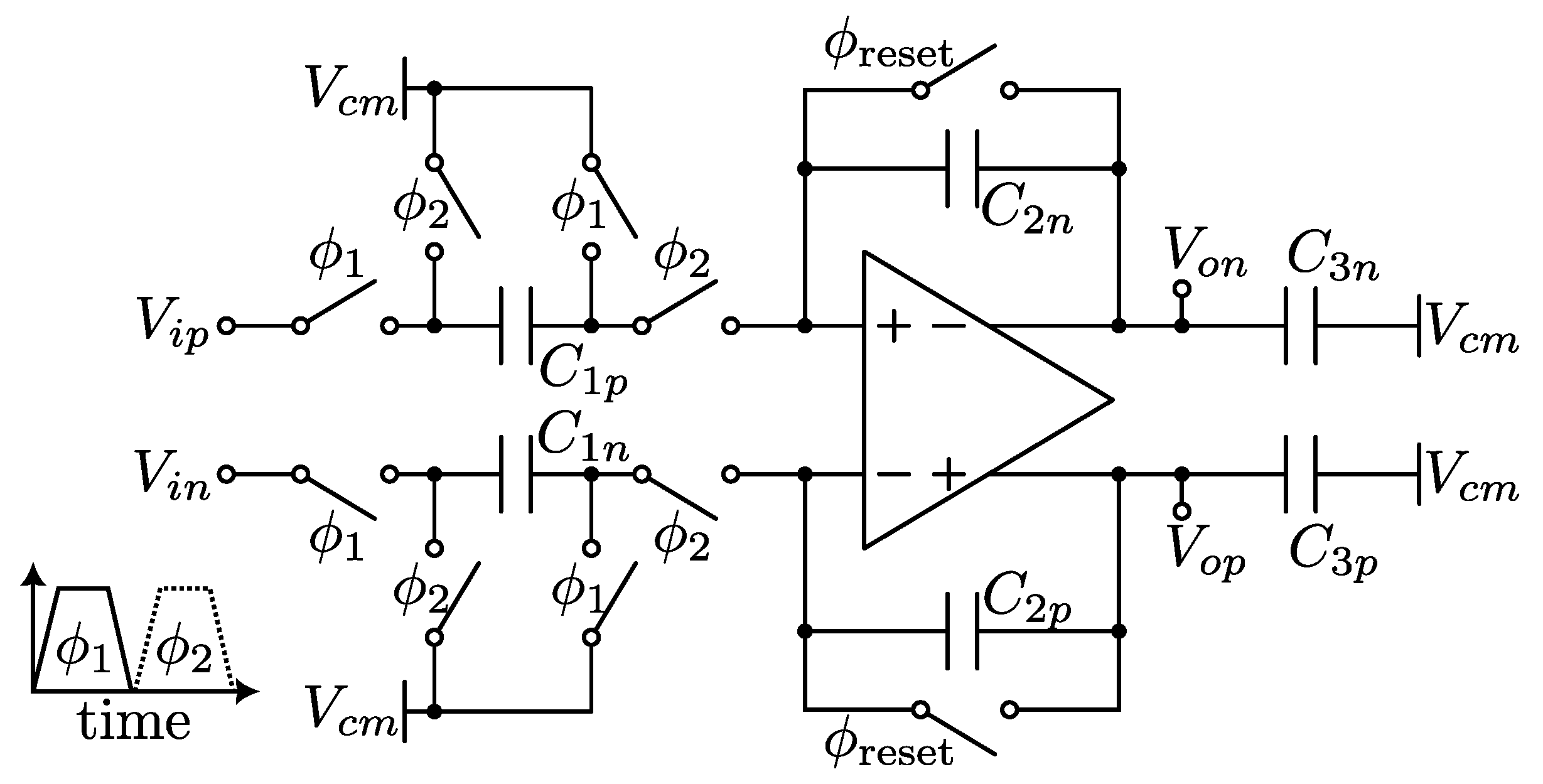
- High-linearity capacitors, ranging from few tens of femto-farads to hundreds of pico-farads, can be reliably realized in CMOS technologies, either as metal-insulator-metal (MIM) or metal-oxide-metal (MOM) structures.
- Versatile switches are realized with MOS transistors.
- The amplifiers involved in the SC circuits are loaded capacitively, hence simple Operational Transconductance Amplifier (OTA) structures are employed with respect to general-purpose Operational Amplifier (OpAmp) circuits.
- MOS devices at the input of the amplifiers do not draw DC bias currents, and hence charge transfer is precisely controlled over a wide range of clock frequencies.
- In contrast to traditional time-continuous operation, the SC approach offers discrete-time signal processing. The impact of non-linearity effects on the precision of the system is minimal, considering that system precision is evaluated at the end of discrete time phases, during which the amplifier output should be able to settle. The settling performance is often evaluated at the end of each phase, in terms of relative error with respect to an ideal response, determined by a capacitance ratio. Conversely, in continuous-time systems, non-linearity effects must be minimized throughout the entire transient duration. This distinction is crucial in making design choices for SC circuits, where non-linear circuit schemes are often adopted.
- Reduce charge injections resulting from transitions in the control signals that command the switches [8].
- Minimize noise introduced during signal processing in the charge domain [9]. At the same time, maximize the maximum input signal to improve the signal-to-distortion and noise ratio of the system.
- Settling speed is often traded with power consumption: numerous advanced circuital techniques have been proposed in the literature to obtain more beneficial balance.
2. Settling Time and Power Optimization
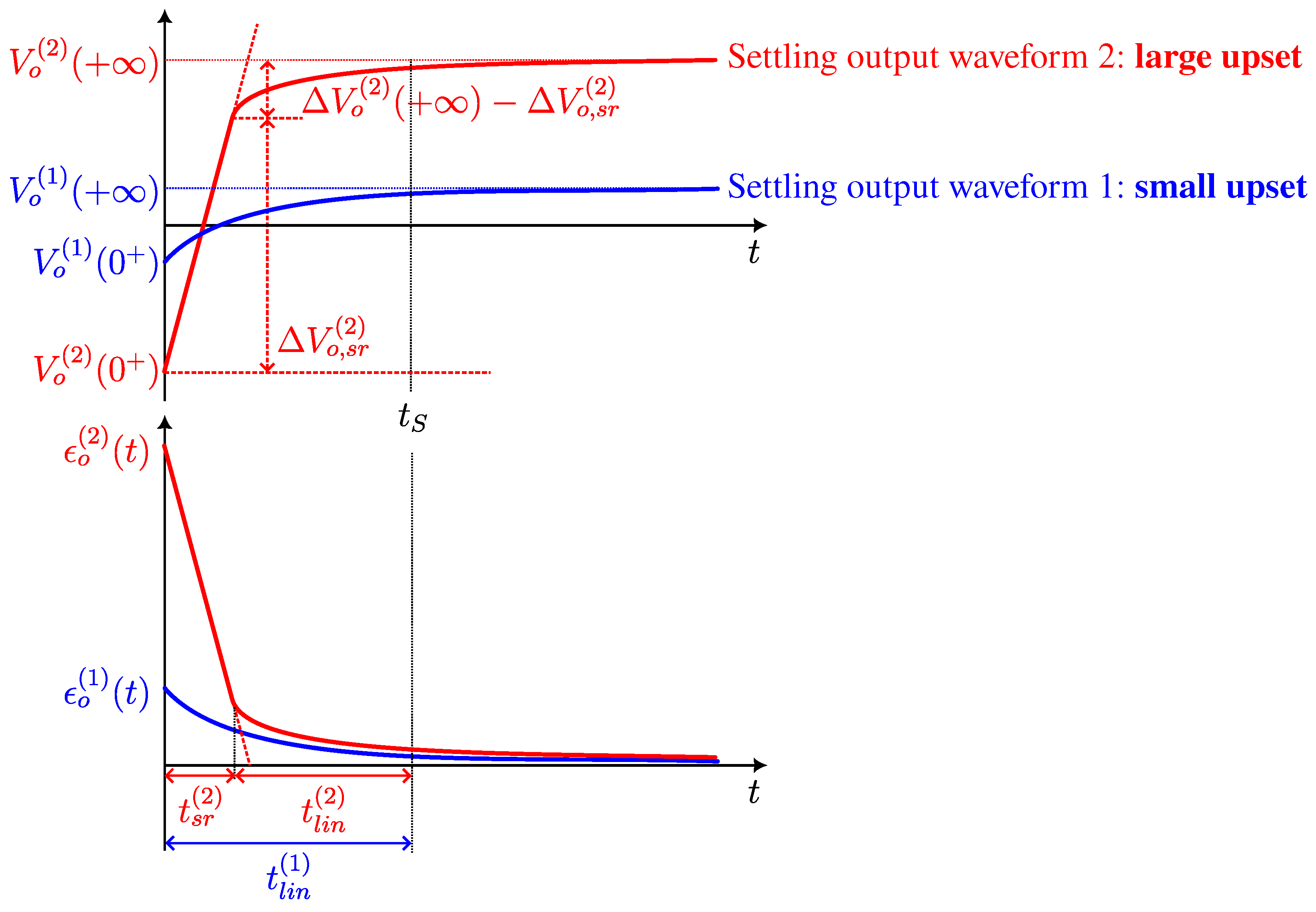
- (i)
- a small output voltage upset, denoted as ;
- (ii)
- a large output voltage upset, denoted as .
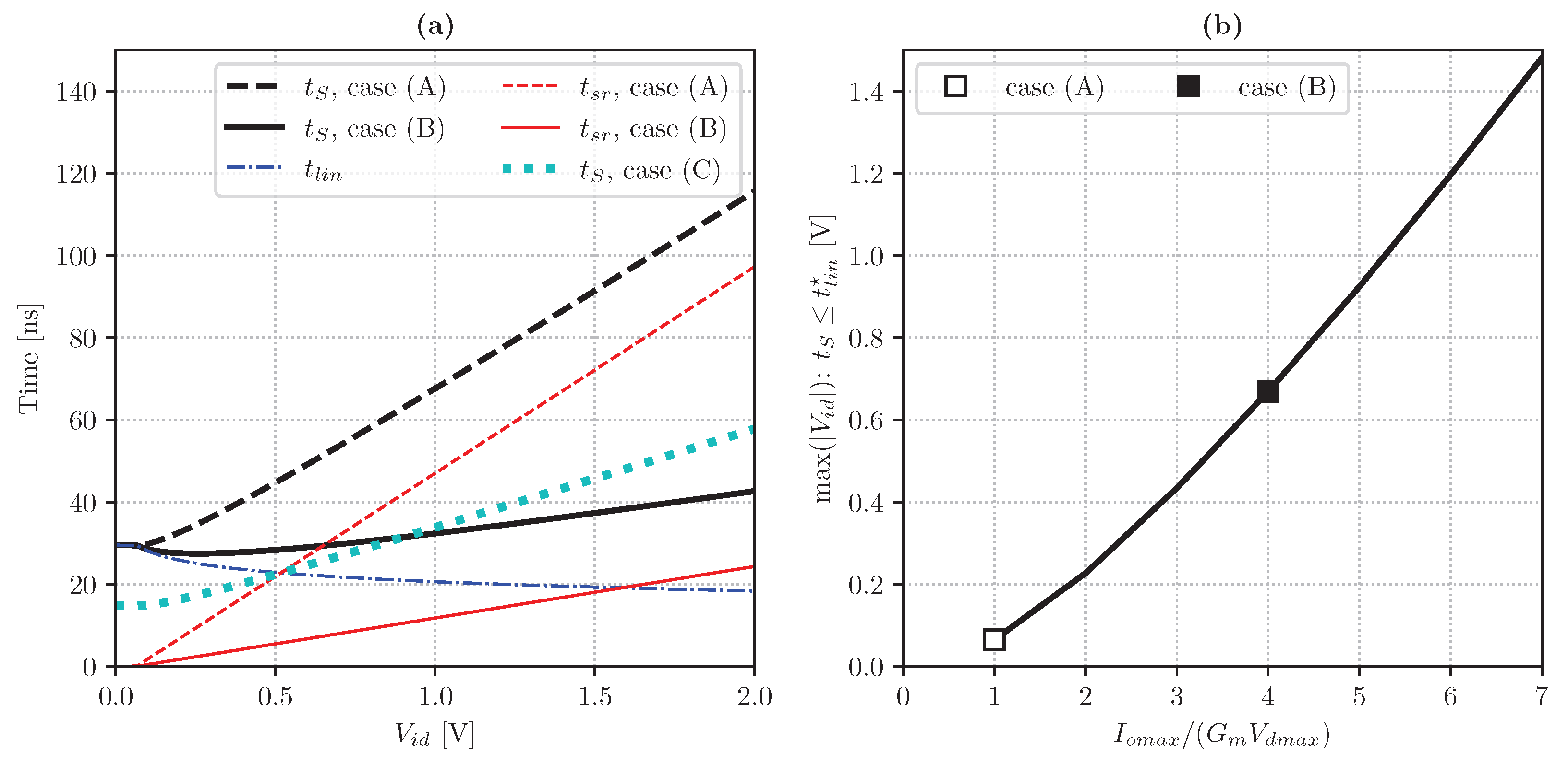
- In the initial region, denoted by , the output voltage () shows its maximum slope (), which in this phase is practically independent of the input signal.
- In the subsequent region, as approaches its final value , the behavior resembles that of scenario (i).
- The term reflects the residual voltage interval to be covered by the OTA after it ends the slewing phase. In this term, corresponds to the portion of the voltage upset related to the slewing phase, , also indicated in Figure 2. Intuitively, results in a decreasing function of , since the residual voltage tends to very small values as is increased. However, will never be zero, since a certain amount of linear settling is always due. Notably, results are inversely proportional to , and hence does not depend on the design choices related to .
- The most important term in (12) is represented by the exponential grow determined by the ratio, causing distortion to rapidly grow with , regardless of the partial compensation due to the term.
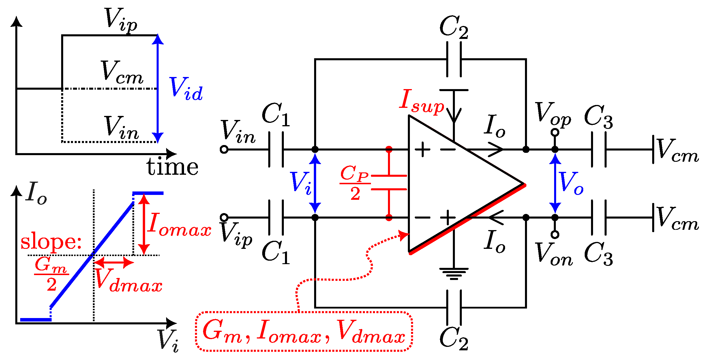
2.1. Simplified Settling Model
- Abrupt transitions between the slew-rate and linear regions.
- Oversimplified modeling of and .
- Inability to capture the effects of non-dominant singularities associated with OTA internal nodes (The presence of non-dominant singularities is typically addressed by introducing the phase margin parameter. In an ideal one-pole system, the phase margin assumes a value of 90 degrees. In practical designs, a phase margin degradation of up to 20 degrees is often tolerable without significantly affecting settling time. This aspect is discussed in Section 2.2 when two-stage architectures are introduced).
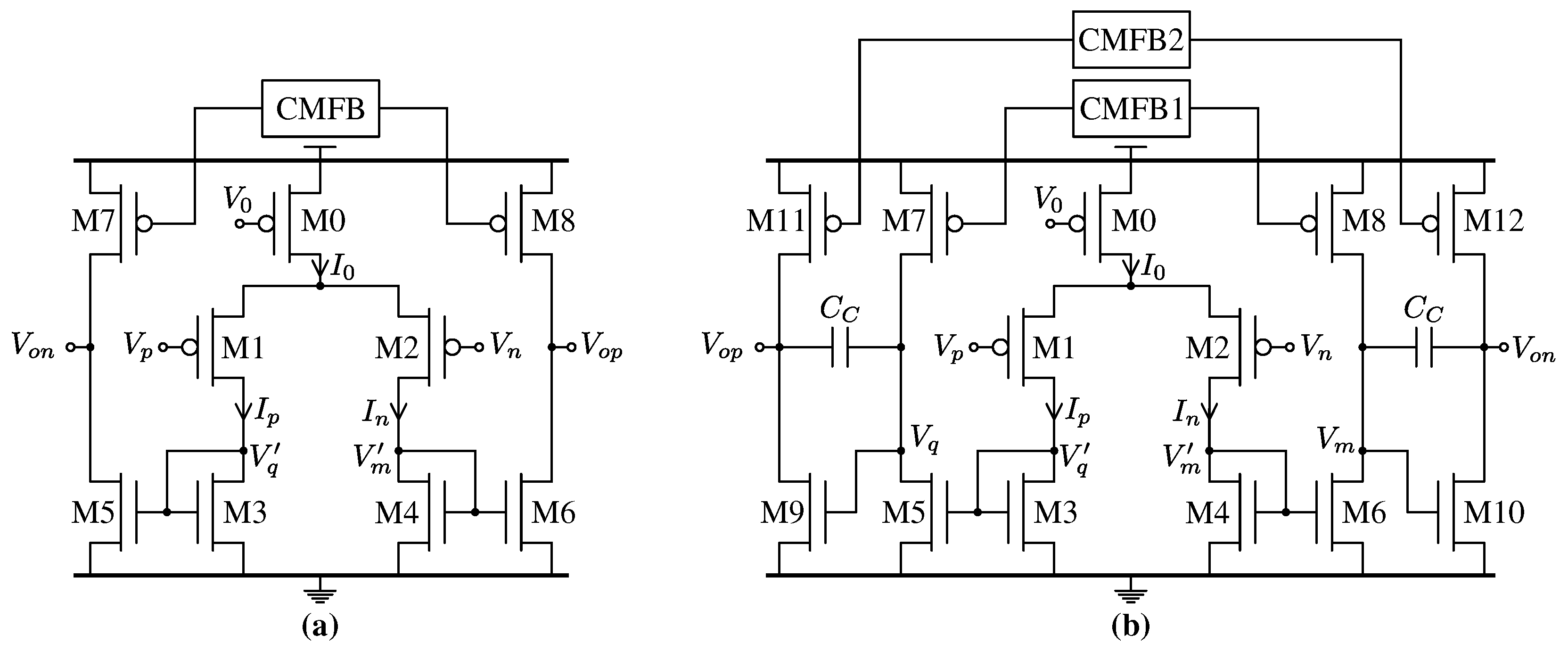
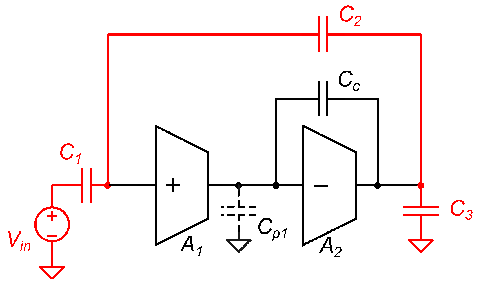
2.2. Considerations on Single-Stage and Two-Stage OTA Architectures
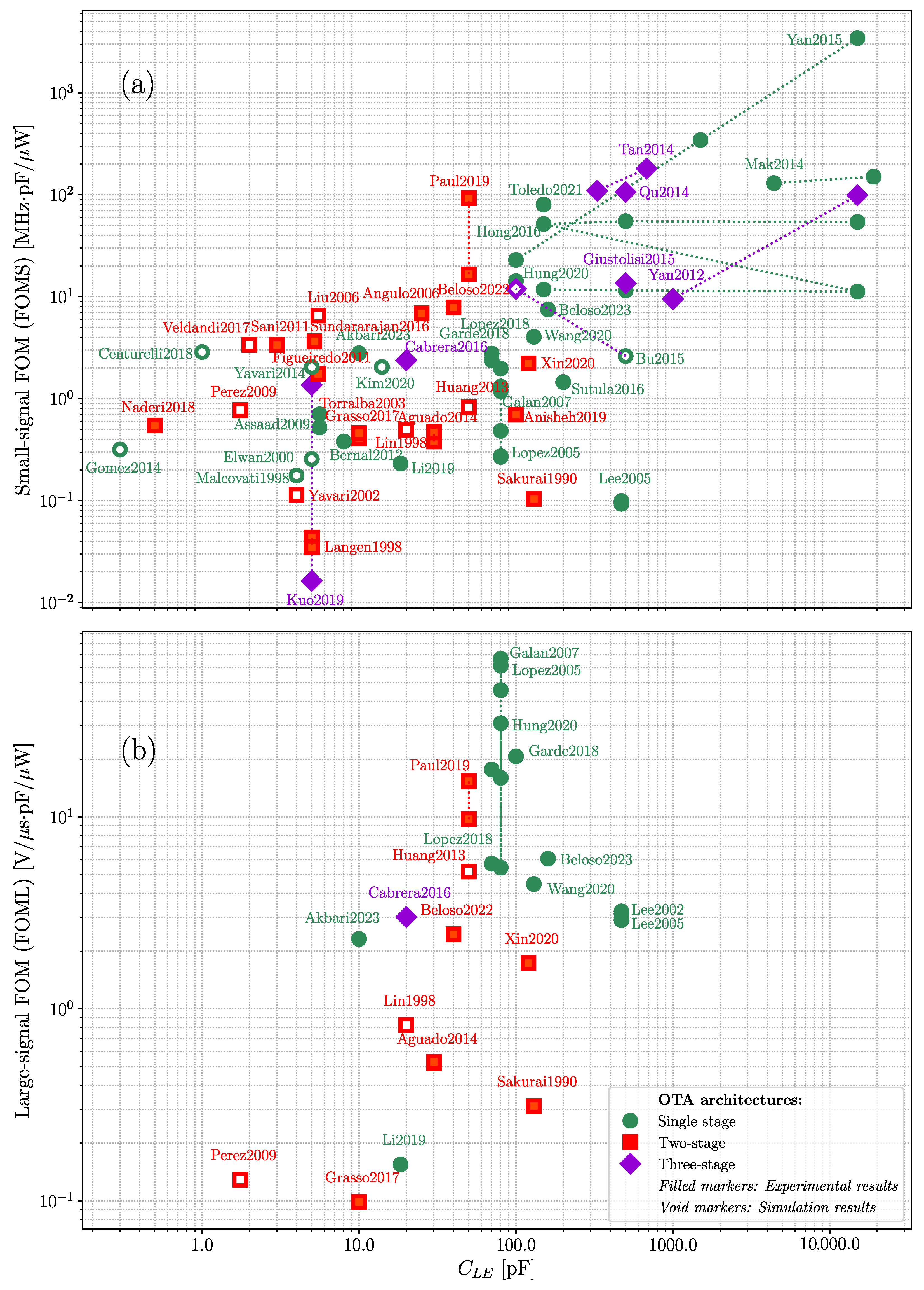
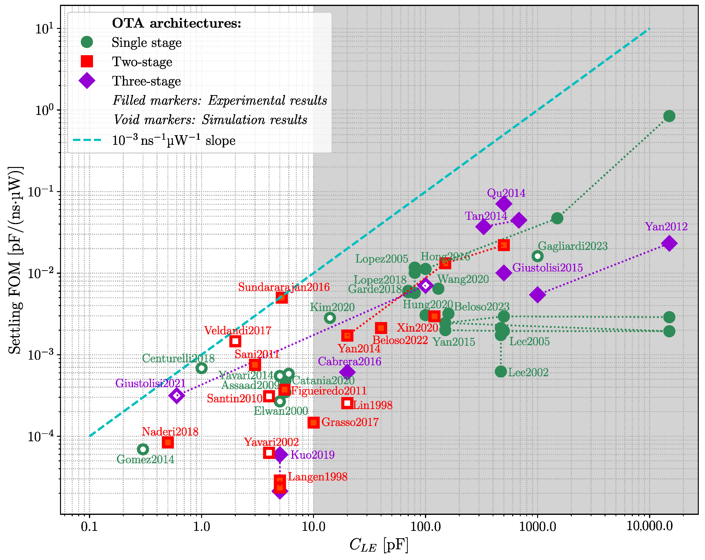
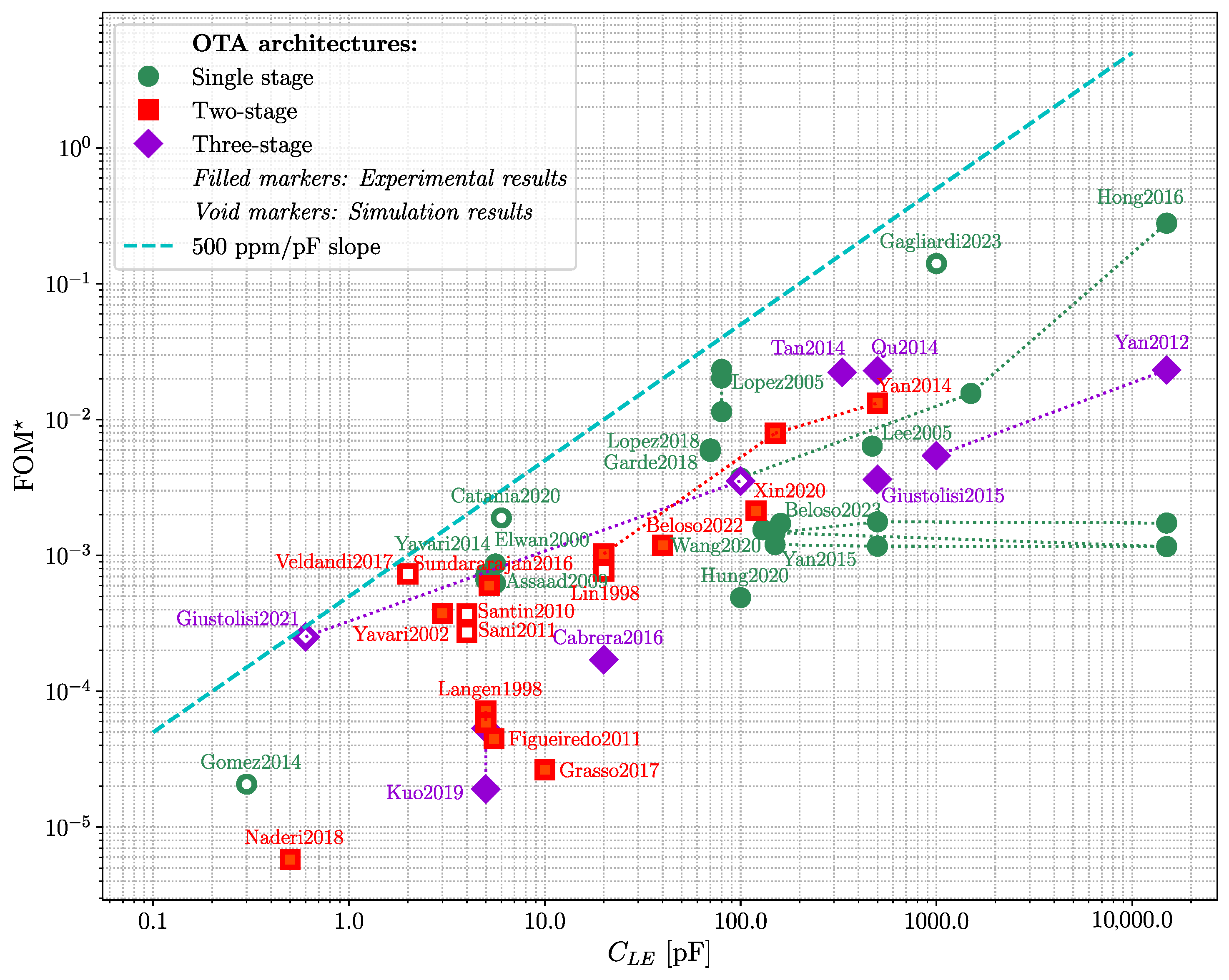
2.3. Figures of Merit (FoMs)
3. Advanced OTAs
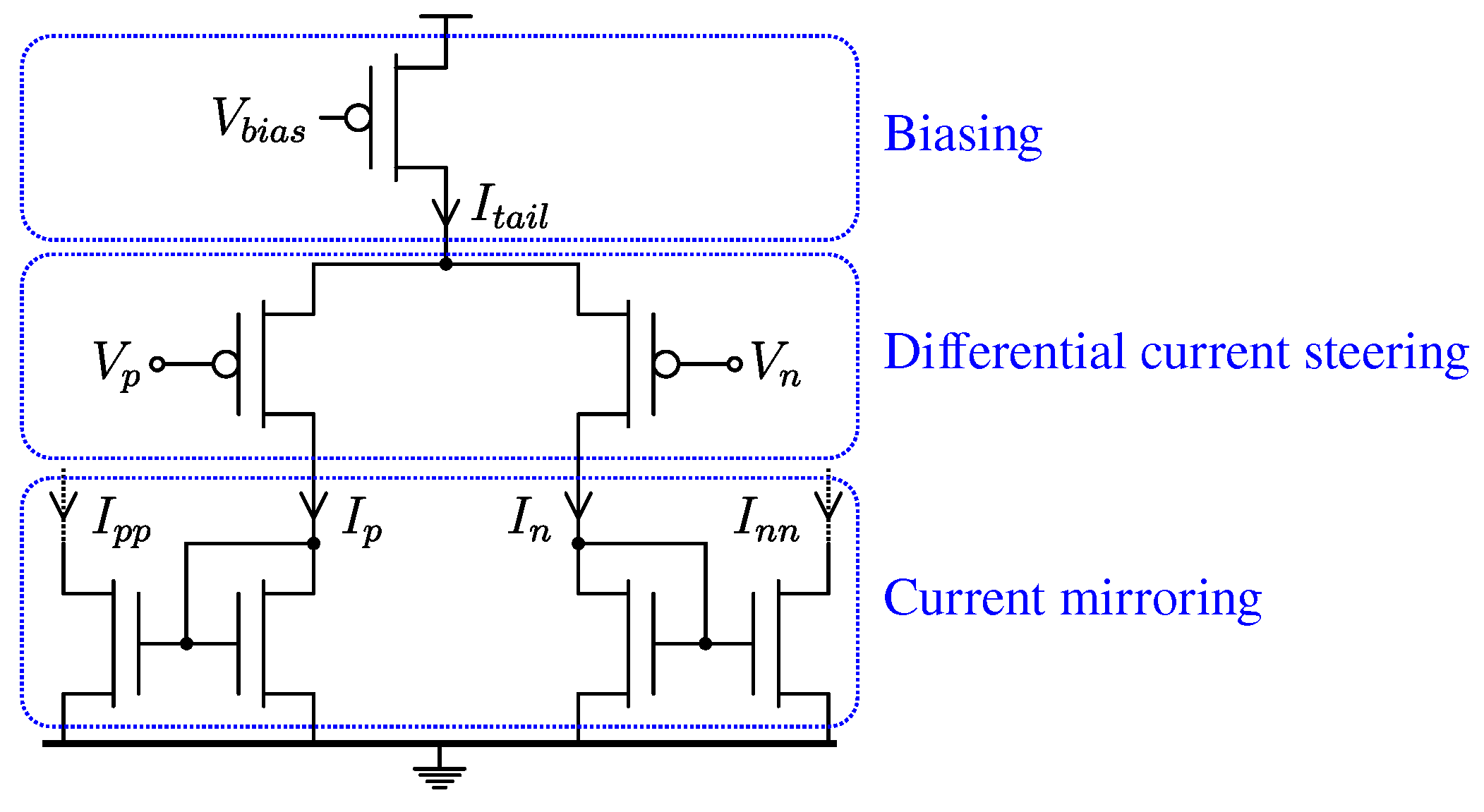
3.1. Cells and Methods for OTA Enhancement
3.2. Flipped Voltage Follower (FVF) Cell
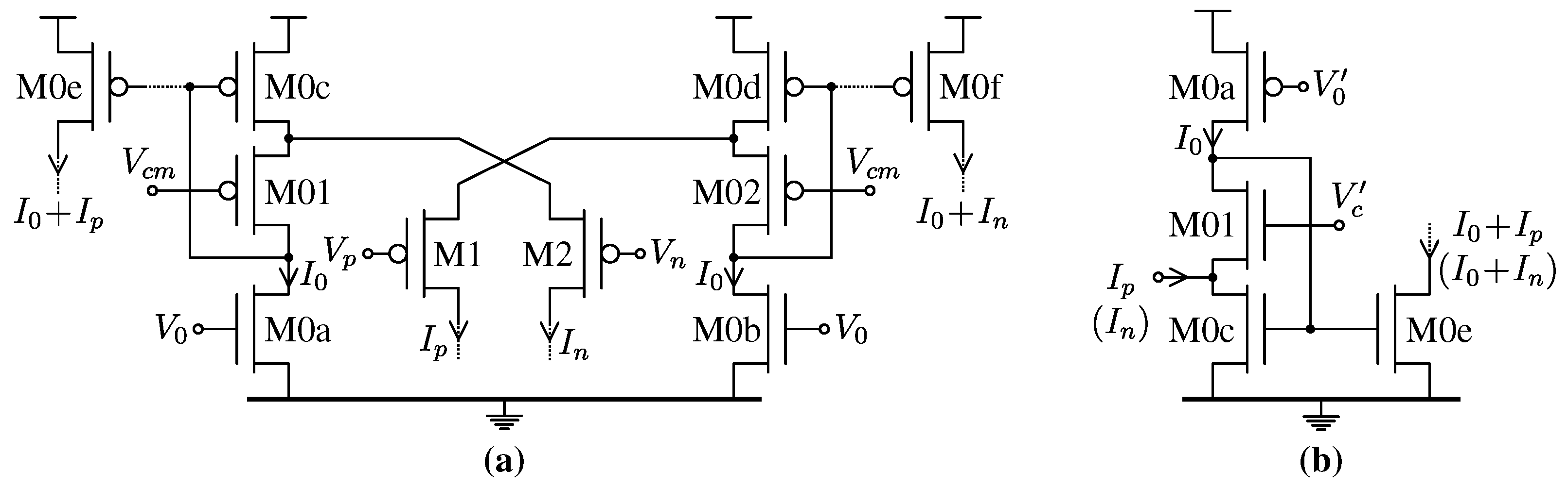
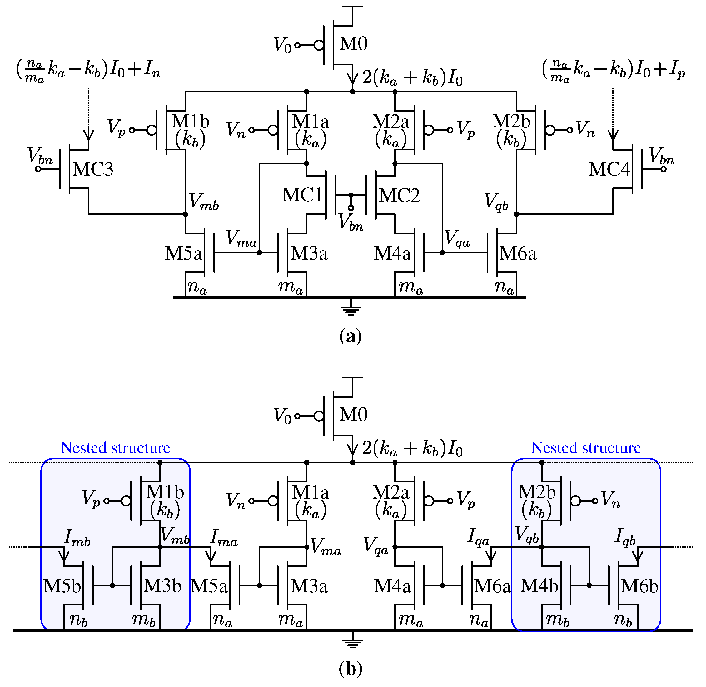
3.3. Current Recycling and Mirror Nesting
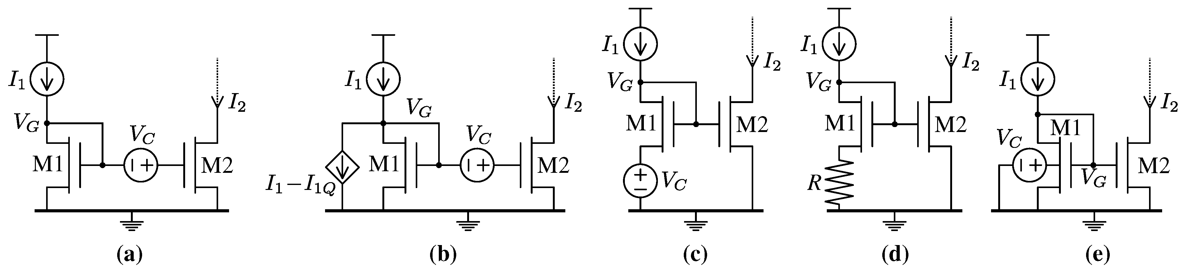
3.4. Non-Linear Current Mirrors
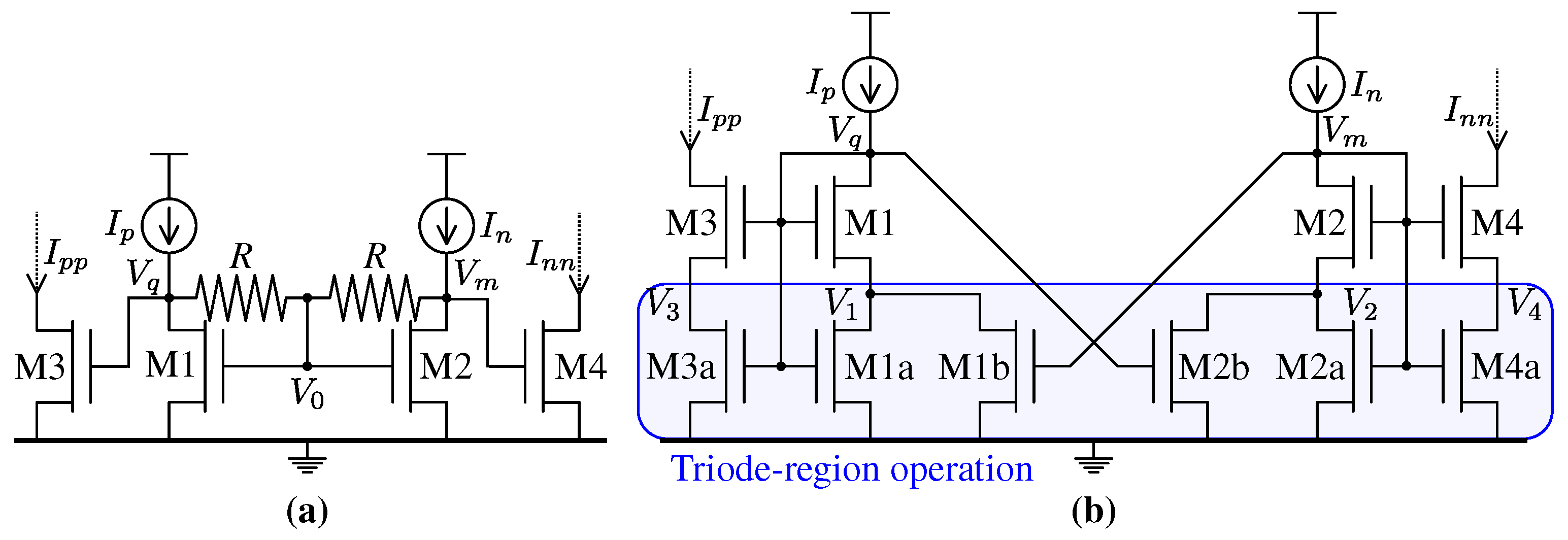
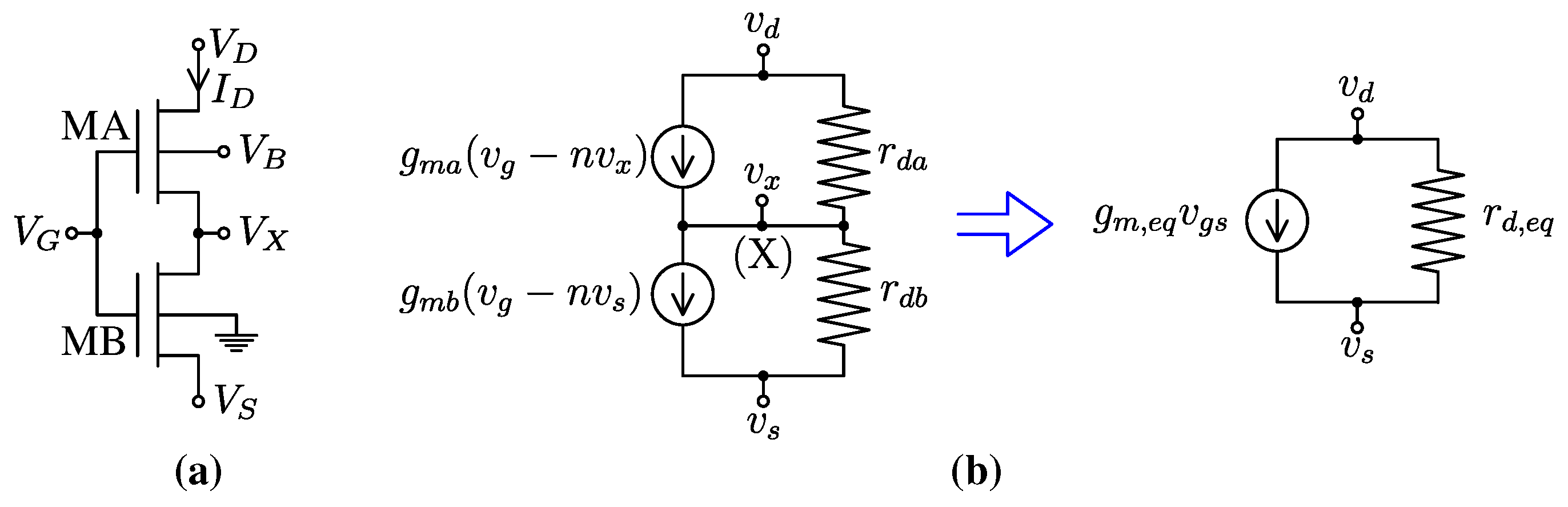
3.5. Compound Body-Biased Mosfets
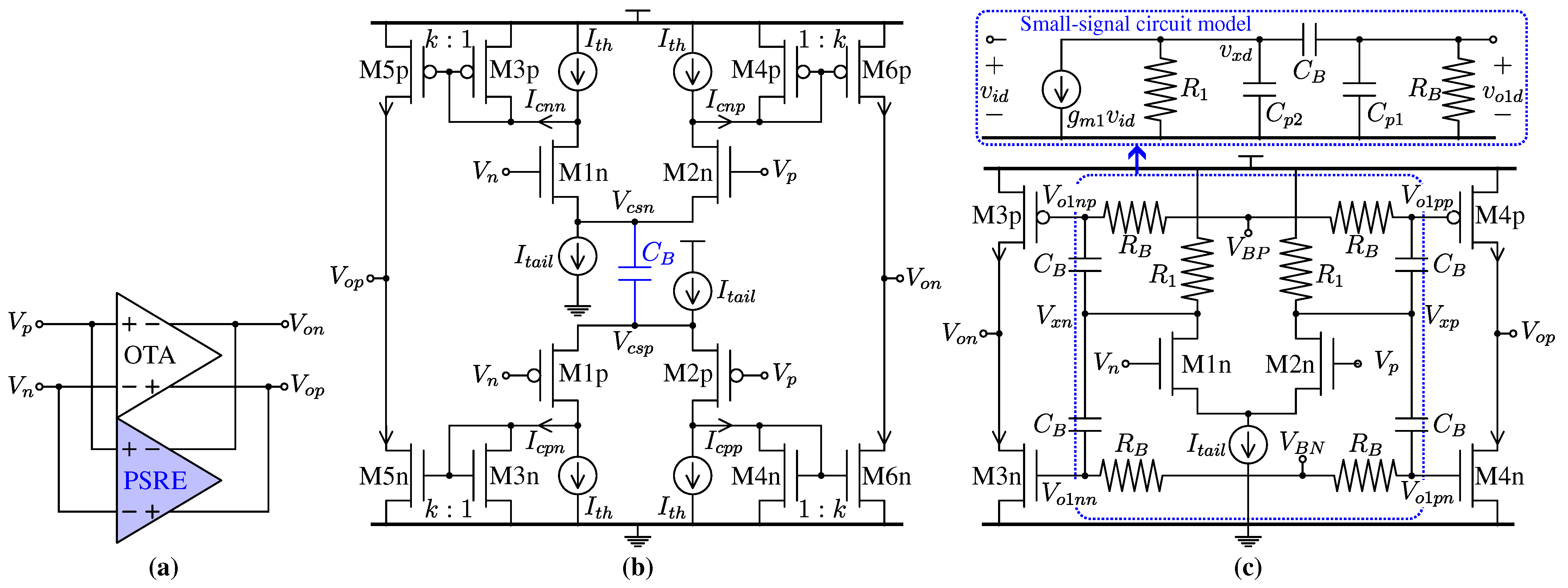
3.6. Parallel-Type Slew-Rate Enhancer (PSRE)
4. Conclusions
Author Contributions
Funding
Conflicts of Interest
References
- Gregorian, R.; Martin, K.W.; Temes, G.C. Switched-capacitor circuit design. Proc. IEEE 1983, 71, 941–966. [Google Scholar] [CrossRef]
- Murmann, B. Thermal Noise in Track-and-Hold Circuits: Analysis and Simulation Techniques. IEEE Solid-State Circuits Mag. 2012, 4, 46–54. [Google Scholar] [CrossRef]
- Schreier, R.; Temes, G.C. Understanding Delta-Sigma Data Converters; John Wiley & Sons: Hoboken, NJ, USA, 2017. [Google Scholar]
- De la Rosa, J.M. Sigma-Delta Converters: Practical Design Guide; John Wiley & Sons: Hoboken, NJ, USA, 2018. [Google Scholar]
- Chris, T.; Moschytz, G.S.; Gilbert, B. (Eds.) Trade-Offs in Analog Circuit Design: The Designer’s Companion; Springer Science & Business Media: Berlin/Heidelberg, Germany, 2004. [Google Scholar]
- Martin, K.; Sedra, A. Effects of the op amp finite gain and bandwidth on the performance of switched-capacitor filters. IEEE Trans. Circuits Syst. 1981, 28, 822–829. [Google Scholar] [CrossRef]
- Temes, G.C. Finite amplifier gain and bandwidth effects in switched-capacitor filters. IEEE J. Solid-State Circuits 1980, 15, 358–361. [Google Scholar] [CrossRef]
- Wegmann, G.; Vittoz, E.A.; Rahali, F. Charge injection in analog MOS switches. IEEE J. Solid-State Circuits 1987, 22, 1091–1097. [Google Scholar] [CrossRef]
- Schreier, R.; Silva, J.; Steensgaard, J.; Temes, G.C. Design-oriented estimation of thermal noise in switched-capacitor circuits. IEEE Trans. Circuits Syst. I Regul. Pap. 2005, 52, 2358–2368. [Google Scholar] [CrossRef]
- Temes, G.C. The Compensation of Amplifier Offset and Finite-Gain Effects in Switched-Capacitor Circuits. Period. Polytech. Electr. Eng. 1986, 30, 147–157. [Google Scholar]
- Razavi, B. The Switched-Capacitor Integrator [A Circuit for All Seasons]. IEEE Solid-State Circuits Mag. 2017, 9, 9–11. [Google Scholar] [CrossRef]
- Wang, F.; Harjani, R. An improved model for the slewing behavior of opamps. IEEE Trans. Circuits Syst. II Analog. Digit. Signal Process. 1995, 42, 679–681. [Google Scholar] [CrossRef]
- Malcovati, P.; Brigati, S.; Francesconi, F.; Maloberti, F.; Cusinato, P.; Baschirotto, A. Behavioral modeling of switched-capacitor sigma-delta modulators. IEEE Trans. Circuits Syst. I Fundam. Theory Appl. 2003, 50, 352–364. [Google Scholar] [CrossRef]
- Yavari, M.; Maghari, N.; Shoaei, O. An accurate analysis of slew rate for two-stage CMOS opamps. IEEE Trans. Circuits Syst. II Express Briefs 2005, 52, 164–167. [Google Scholar] [CrossRef]
- Catania, A.; Cicalini, M.; Dei, M.; Piotto, M.; Bruschi, P. Performance Analysis and Design Optimization of Parallel-Type Slew-Rate Enhancers for Switched-Capacitor Applications. Electronics 2020, 9, 1949. [Google Scholar] [CrossRef]
- Kareppagoudr, M.; Shakya, J.; Caceres, E.; Kuo, Y.W.; Temes, G.C. Slewing mitigation technique for switched capacitor circuits. IEEE Trans. Circuits Syst. I Regul. Pap. 2020, 67, 3251–3261. [Google Scholar] [CrossRef]
- Giustolisi, G.; Palumbo, G. Design of Three-Stage OTA Based on Settling-Time Requirements Including Large and Small Signal Behavior. IEEE Trans. Circuits Syst. I Regul. Pap. 2021, 68, 998–1011. [Google Scholar] [CrossRef]
- Catania, A.; Cicalini, M.; Piotto, M.; Bruschi, P.; Dei, M. Energy Efficiency in Slew-Rate Enhanced Single-Stage OTAs for Switched-Capacitor Applications. J. Low Power Electron. Appl. 2021, 11, 1. [Google Scholar] [CrossRef]
- Oliaei, O. Sigma-delta modulator with spectrally shaped feedback. IEEE Trans. Circuits Syst. II Analog. Digit. Signal Process. 2003, 50, 518–530. [Google Scholar] [CrossRef]
- Enz, C.C. MOS Translinear Modeling Dedicated to Low-Current and Low-Voltage Analog Circuit Design and Simulation. 1995. Available online: http://ekv.epfl.ch (accessed on 10 April 2024).
- Ruiz-Amaya, J.; Delgado-Restituto, M.; Rodriguez-Vazquez, Á. Accurate Settling-Time Modeling and Design Procedures for Two-Stage Miller-Compensated Amplifiers for Switched-Capacitor Circuits. IEEE Trans. Circuits Syst. I Regul. Pap. 2009, 56, 1077–1087. [Google Scholar] [CrossRef]
- Nguyen, R.; Murmann, B. The Design of Fast-Settling Three-Stage Amplifiers Using the Open-Loop Damping Factor as a Design Parameter. IEEE Trans. Circuits Syst. I Regul. Pap. 2010, 57, 1244–1254. [Google Scholar] [CrossRef]
- Giustolisi, G.; Palumbo, G. Design of CMOS three-stage amplifiers for near-to-minimum settling-time. Microelectron. J. 2021, 107, 104939. [Google Scholar] [CrossRef]
- Seth, S.; Murmann, B. Settling Time and Noise Optimization of a Three-Stage Operational Transconductance Amplifier. IEEE Trans. Circuits Syst. I Regul. Pap. 2013, 60, 1168–1174. [Google Scholar] [CrossRef]
- Monticelli, D. A quad CMOS single-supply opamp with rail-to rail output swing. In Proceedings of the 1986 IEEE International Solid-State Circuits Conference, Digest of Technical Papers, Anaheim, CA, USA, 19–21 February 1986; pp. 18–19. [Google Scholar] [CrossRef]
- Langen, K.-J.D.; Huijsing, J.H. Compact low-voltage power-efficient operational amplifier cells for VLSI. IEEE J. Solid-State Circuits 1998, 33, 1482–1496. [Google Scholar] [CrossRef]
- Carvajal, R.; Torralba, A.; Tombs, J.; Muñoz, F.; Ramírez-Angulo, J. Low voltage class AB output stage for CMOS Op-Amps using multiple input floating gate transistors. J. Analog Integr. Circuits Signal Process. 2003, 36, 245–249. [Google Scholar] [CrossRef]
- Sansen, W.M. Analog Design Essentials; Springer Science & Business Media: Berlin/Heidelberg, Germany, 2007; Volume 859. [Google Scholar]
- Palumbo, G.; Pennisi, S. Feedback Amplifiers: Theory and Design; Springer Science & Business Media: Berlin/Heidelberg, Germany, 2002. [Google Scholar]
- Beloso-Legarra, J.; De La Cruz-Blas, C.A.; Lopez-Martin, A.J. Power-Efficient Single-Stage Class-AB OTA Based on Non-Linear Nested Current Mirrors. IEEE Trans. Circuits Syst. I Regul. Pap. 2023, 70, 1566–1579. [Google Scholar] [CrossRef]
- Akbari, M.; Hussein, S.M.; Hashim, Y.; Khateb, F.; Kulej, T.; Tang, K.-T. Implementation of a Multipath Fully Differential OTA in 0.18-μm CMOS Process. IEEE Trans. Very Large Scale Integr. VLSI Syst. 2023, 31, 147–151. [Google Scholar] [CrossRef]
- Kim, J.; Song, S.; Roh, J. A High Slew-Rate Enhancement Class-AB Operational Transconductance Amplifier (OTA) for Switched-Capacitor (SC) Applications. IEEE Access 2020, 8, 226167–226175. [Google Scholar] [CrossRef]
- Hung, C.H.; Zheng, Y.; Guo, J.; Leung, K.N. Bandwidth and Slew Rate Enhanced OTA with Sustainable Dynamic Bias. IEEE Trans. Circuits Syst. II Express Briefs 2020, 67, 635–639. [Google Scholar] [CrossRef]
- Anisheh, S.M.; Abbasizadeh, H.; Shamsi, H.; Dadkhah, C.; Lee, K.-Y. 98-dB Gain Class-AB OTA with 100 pF Load Capacitor in 180-nm Digital CMOS Process. IEEE Access 2019, 7, 17772–17779. [Google Scholar] [CrossRef]
- Sutula, S.; Dei, M.; Terés, L.; Serra-Graells, F. Variable-Mirror Amplifier: A New Family of Process-Independent Class-AB Single-Stage OTAs for Low-Power SC Circuits. IEEE Trans. Circuits Syst. I Regul. Pap. 2016, 63, 1101–1110. [Google Scholar] [CrossRef]
- Yan, Z.; Mak, P.-I.; Law, M.-K.; Martins, R.P.; Maloberti, F. Nested-Current-Mirror Rail-to-Rail-Output Single-Stage Amplifier with Enhancements of DC Gain, GBW and Slew Rate. IEEE J. Solid-State Circuits 2015, 50, 2353–2366. [Google Scholar] [CrossRef]
- Aguado-Ruiz, J.; Lopez-Martin, A.; Lopez-Lemus, J.; Ramirez-Angulo, J. Power Efficient Class AB Op-Amps with High and Symmetrical Slew Rate. IEEE Trans. Very Large Scale Integr. VLSI Syst. 2014, 22, 943–947. [Google Scholar] [CrossRef]
- Galan, J.A.; Lopez-Martin, A.J.; Carvajal, R.G.; Ramirez-Angulo, J.; Rubia-Marcos, C. Super Class-AB OTAs with Adaptive Biasing and Dynamic Output Current Scaling. IEEE Trans. Circuits Syst. I Regul. Pap. 2007, 54, 449–457. [Google Scholar] [CrossRef]
- Lopez-Martin, A.J.; Baswa, S.; Ramirez-Angulo, J.; Carvajal, R.G. Low-Voltage Super class AB CMOS OTA cells with very high slew rate and power efficiency. IEEE J. Solid-State Circuits 2005, 40, 1068–1077. [Google Scholar] [CrossRef]
- Hong, S.-W.; Cho, G.-H. A Pseudo Single-Stage Amplifier with an Adaptively Varied Medium Impedance Node for Ultra-High Slew Rate and Wide-Range Capacitive-Load Drivability. IEEE Trans. Circuits Syst. I Regul. Pap. 2016, 63, 1567–1578. [Google Scholar] [CrossRef]
- Lopez-Martin, A.J.; Garde, M.P.; Algueta, J.M.; de la Cruz Blas, C.A.; Carvajal, R.G.; Ramirez-Angulo, J. Enhanced Single-Stage Folded Cascode OTA Suitable for Large Capacitive Loads. IEEE Trans. Circuits Syst. II Express Briefs 2018, 65, 441–445. [Google Scholar] [CrossRef]
- Garde, M.P.; Lopez-Martin, A.; Carvajal, R.G.; Ramírez-Angulo, J. Super Class-AB Recycling Folded Cascode OTA. IEEE J. Solid-State Circuits 2018, 53, 2614–2623. [Google Scholar] [CrossRef]
- Wang, Y.; Zhang, Q.; Yu, S.S.; Zhao, X.; Trinh, H.; Shi, P. A Robust Local Positive Feedback Based Performance Enhancement Strategy for Non-Recycling Folded Cascode OTA. IEEE Trans. Circuits Syst. I Regul. Pap. 2020, 67, 2897–2908. [Google Scholar] [CrossRef]
- Toledo, P.; Crovetti, P.; Aiello, O.; Alioto, M. Design of Digital OTAs with Operation Down to 0.3 V and nW Power for Direct Harvesting. IEEE Trans. Circuits Syst. I Regul. Pap. 2021, 68, 3693–3706. [Google Scholar] [CrossRef]
- Xin, Y.; Zhao, X.; Wen, B.; Dong, L.; Lv, X. A High Current Efficiency Two-Stage Amplifier with Inner Feedforward Path Compensation Technique. IEEE Access 2020, 8, 22664–22671. [Google Scholar] [CrossRef]
- Centurelli, F.; Monsurrò, P.; Parisi, G.; Tommasino, P.; Trifiletti, A. A Topology of Fully Differential Class-AB Symmetrical OTA with Improved CMRR. IEEE Trans. Circuits Syst. II Express Briefs 2018, 65, 1504–1508. [Google Scholar] [CrossRef]
- Grasso, A.D.; Pennisi, S.; Scotti, G.; Trifiletti, A. 0.9-V Class-AB Miller OTA in 0.35-μm CMOS with Threshold-Lowered Non-Tailed Differential Pair. IEEE Trans. Circuits Syst. I Regul. Pap. 2017, 64, 1740–1747. [Google Scholar] [CrossRef]
- Cabrera-Bernal, E.; Pennisi, S.; Grasso, A.D.; Torralba, A.; Carvajal, R.G. 0.7-V Three-Stage Class-AB CMOS Operational Transconductance Amplifier. IEEE Trans. Circuits Syst. I Regul. Pap. 2016, 63, 1807–1815. [Google Scholar] [CrossRef]
- Assaad, R.S.; Silva-Martinez, J. The Recycling Folded Cascode: A General Enhancement of the Folded Cascode Amplifier. IEEE J. Solid-State Circuits 2009, 44, 2535–2542. [Google Scholar] [CrossRef]
- Kuo, P.-Y.; Tsai, S.-D. An Enhanced Scheme of Multi-Stage Amplifier with High-Speed High-Gain Blocks and Recycling Frequency Cascode Circuitry to Improve Gain-Bandwidth and Slew Rate. IEEE Access 2019, 7, 130820–130829. [Google Scholar] [CrossRef]
- Lee, H.; Mok, P.K.T.; Leung, K.N. Design of low-power analog drivers based on slew-rate enhancement circuits for CMOS low-dropout regulators. IEEE Trans. Circuits Syst. II Express Briefs 2005, 52, 563–567. [Google Scholar] [CrossRef]
- Naderi, M.H.; Prakash, S.; Silva-Martinez, J. Operational Transconductance Amplifier with Class-B Slew-Rate Boosting for Fast High-Performance Switched-Capacitor Circuits. IEEE Trans. Circuits Syst. I Regul. Pap. 2018, 65, 3769–3779. [Google Scholar] [CrossRef]
- Malcovati, P.; Maloberti, F.; Terzani, M. An high-swing, 1.8 V, push-pull opamp for sigma-delta modulators. In Proceedings of the 1998 IEEE International Conference on Electronics, Circuits and Systems, Lisboa, Portugal, 7–10 September 1998; Volume 1, pp. 33–36. [Google Scholar] [CrossRef]
- Elwan, H.; Gao, W.; Sadkowski, R.; Ismail, M. A low voltage CMOS class AB operational transconductance amplifier. In Proceedings of the 1999 IEEE International Symposium on Circuits and Systems (ISCAS), Orlando, FL, USA, 30 May–2 June 1999; Volume 2, pp. 632–635. [Google Scholar] [CrossRef]
- Yavari, M.; Shoaei, O. Very low-voltage, low-power and fast-settling OTA for switched-capacitor applications. In Proceedings of the 14th International Conference on Microelectronics, Beirut, Lebanon, 13 December 2002; pp. 10–13. [Google Scholar] [CrossRef]
- Torralba, A.; Carvajal, R.; Ramírez-Angulo, J.; Tombs, J.; Muñoz, F.; Galan, J. Class AB output stages for low voltage CMOS Opamps with accurate quiescent current control by means of dynamic biasing. J. Analog Integr. Circuits Signal Process. 2003, 36, 69–77. [Google Scholar] [CrossRef]
- Liu, A.; Yang, H. Low Voltage Low Power Class-AB OTA with Negative Resistance Load. In Proceedings of the 2006 International Conference on Communications, Circuits and Systems, Guilin, China, 25–28 June 2006; pp. 2251–2254. [Google Scholar] [CrossRef]
- Ramirez-Angulo, J.; Carvajal, R.G.; Galan, J.A.; Lopez-Martin, A. A free but efficient low-voltage class-AB two-stage operational amplifier. IEEE Trans. Circuits Syst. II Express Briefs 2006, 53, 568–571. [Google Scholar] [CrossRef]
- Perez, A.P.; Kumar, Y.B.N.; Bonizzoni, E.; Maloberti, F. Slew-rate and gain enhancement in two stage operational amplifiers. In Proceedings of the 2009 IEEE International Symposium on Circuits and Systems (ISCAS), Taipei, Taiwan, 24–27 May 2009; pp. 2485–2488. [Google Scholar] [CrossRef]
- Figueiredo, M.; Santos-Tavares, R.; Santin, E.; Ferreira, J.; Evans, G.; Goes, J. A Two-Stage Fully Differential Inverter-Based Self-Biased CMOS Amplifier with High Efficiency. IEEE Trans. Circuits Syst. I Regul. Pap. 2011, 58, 1591–1603. [Google Scholar] [CrossRef]
- Yavari, M.; Moosazadeh, T. A single-stage operational amplifier with enhanced transconductance and slew rate for switched-capacitor circuits. Analog. Integr. Circ. Sig. Process. 2014, 79, 589–598. [Google Scholar] [CrossRef]
- Yan, Z.; Mak, P.-I.; Law, M.-K.; Martins, R. A 0.016 mm2 144 μW three-stage amplifier capable of driving 1-to-15 nF capacitive load with >0.95 MHz GBW. In Proceedings of the 2012 IEEE International Solid-State Circuits Conference, San Francisco, CA, USA, 19–23 February 2012; pp. 368–370. [Google Scholar] [CrossRef]
- Qu, W.; Im, J.-P.; Kim, H.-S.; Cho, G.-H. 17.3 A 0.9 V 6.3 μW multistage amplifier driving 500 pF capacitive load with 1.34 MHz GBW. In Proceedings of the 2014 IEEE International Solid-State Circuits Conference Digest of Technical Papers (ISSCC), San Francisco, CA, USA, 9–13 February 2014; pp. 290–291. [Google Scholar] [CrossRef]
- Mak, K.H.; Leung, K.N. A Signal- and Transient-Current Boosting Amplifier for Large Capacitive Load Applications. IEEE Trans. Circuits Syst. I Regul. Pap. 2014, 61, 2777–2785. [Google Scholar] [CrossRef]
- Tan, M.; Ki, W.-H. A Cascode Miller-Compensated Three-Stage Amplifier with Local Impedance Attenuation for Optimized Complex-Pole Control. IEEE J. Solid-State Circuits 2015, 50, 440–449. [Google Scholar] [CrossRef]
- Monticelli, D.M. A quad CMOS single-supply op amp with rail-to-rail output swing. IEEE J. Solid-State Circuits 1986, 21, 1026–1034. [Google Scholar] [CrossRef]
- Sakurai, S.; Zarabadi, S.R.; Ismail, M. Folded-cascode CMOS operational amplifier with slew rate enhancement circuit. In Proceedings of the IEEE International Symposium on Circuits and Systems, New Orleans, LA, USA, 1–3 May 1990; Volume 4, pp. 3205–3208. [Google Scholar] [CrossRef]
- Lin, C.-H.; Ismail, M. A low-voltage CMOS rail-to-rail class-AB input/output opamp with slew-rate and settling enhancement. In Proceedings of the 1998 IEEE International Symposium on Circuits and Systems (ISCAS), Monterey, CA, USA, 31 May–3 June 1998; Volume 1, pp. 448–450. [Google Scholar] [CrossRef]
- Sundararajan, A.D.; Hasan, S.M.R. Quadruply Split Cross-Driven Doubly Recycled gm-Doubling Recycled Folded Cascode for Microsensor Instrumentation Amplifiers. IEEE Trans. Circuits Syst. II Express Briefs 2016, 63, 543–547. [Google Scholar] [CrossRef]
- Lee, H.; Mok, P.K.T. Single-point-detection slew-rate enhancement circuits for single-stage amplifiers. In Proceedings of the 2002 IEEE International Symposium on Circuits and Systems (ISCAS), Phoenix-Scottsdale, AZ, USA, 26–29 May 2002; p. II. [Google Scholar] [CrossRef]
- Bernal, M.R.V.; Celma, S.; Medrano, N.; Calvo, B. An Ultralow-Power Low-Voltage Class-AB Fully Differential OpAmp for Long-Life Autonomous Portable Equipment. IEEE Trans. Circuits Syst. II Express Briefs 2012, 59, 643–647. [Google Scholar] [CrossRef]
- Huang, B.; Xu, L.; Chen, D. Slew rate enhancement via excessive transient feedback. Electron. Lett. 2013, 49, 930–932. [Google Scholar] [CrossRef]
- Bu, S.; Tse, H.W.; Leung, K.N.; Guo, J.; Ho, M. Gain and slew rate enhancement for amplifiers through current starving and feeding. In Proceedings of the 2015 IEEE International Symposium on Circuits and Systems (ISCAS), Lisbon, Portugal, 24–27 May 2015; pp. 2073–2076. [Google Scholar] [CrossRef]
- Giustolisi, G.; Palumbo, G. Efficient Design Strategy for Optimizing the Settling Time in Three-Stage Amplifiers Including Small- and Large-Signal Behavior. Electronics 2021, 10, 612. [Google Scholar] [CrossRef]
- Giustolisi, G.; Palumbo, G. Three-Stage Dynamic-Biased CMOS Amplifier with a Robust Optimization of the Settling Time. IEEE Trans. Circuits Syst. I Regul. Pap. 2015, 62, 2641–2651. [Google Scholar] [CrossRef]
- Veldandi, H.; Shaik, R.A. A 1-V high-gain two-stage self-cascode operational transconductance amplifier. In Proceedings of the 2017 Innovations in Power and Advanced Computing Technologies (i-PACT), Vellore, India, 21–22 April 2017; pp. 1–4. [Google Scholar] [CrossRef]
- Gomez, H.; Espinosa, G. 55 dB DC gain, robust to PVT single-stage fully differential amplifier on 45 nm SOI-CMOS technology. Electron. Lett. 2014, 50, 737–739. [Google Scholar] [CrossRef]
- Taherzadeh-Sani, M.; Hamoui, A.A. A 1-V Process-Insensitive Current-Scalable Two-Stage Opamp with Enhanced DC Gain and Settling Behavior in 65-nm Digital CMOS. IEEE J. Solid-State Circuits 2011, 46, 660–668. [Google Scholar] [CrossRef]
- Santin, E.; Figueiredo, M.; Tavares, R.; Goes, J.; Oliveira, L.B. Fast-settling low-power two-stage self-biased CMOS amplifier using feedforward-regulated cascode devices. In Proceedings of the 2010 17th IEEE International Conference on Electronics, Circuits and Systems, Athens, Greece, 12–15 December 2010; pp. 25–28. [Google Scholar] [CrossRef]
- Yan, Z.; Wang, W.; Mak, P.-I.; Law, M.-K.; Martins, R.P. A 0.0045-mm2 32.4-μW Two-Stage Amplifier for pF-to-nF Load Using CM Frequency Compensation. IEEE Trans. Circuits Syst. II Express Briefs 2015, 62, 246–250. [Google Scholar] [CrossRef]
- Beloso-Legarra, J.; Grasso, A.D.; Lopez-Martin, A.J.; Palumbo, G.; Pennisi, S. Two-Stage OTA with All Subthreshold MOSFETs and Optimum GBW to DC-Current Ratio. IEEE Trans. Circuits Syst. II Express Briefs 2022, 69, 3154–3158. [Google Scholar] [CrossRef]
- Li, X.; Hou, B.; Ju, C.; Wei, Q.; Zhou, B.; Zhang, R. A Complementary Recycling Operational Transconductance Amplifier with Data-Driven Enhancement of Transconductance. Electronics 2019, 8, 1457. [Google Scholar] [CrossRef]
- Gagliardi, F.; Catania, A.; Piotto, M.; Bruschi, P.; Dei, M. A Novel High-Performance Parallel-Type Slew-Rate Enhancer for LCD-Driving Applications. In Proceedings of the 2023 18th Conference on Ph.D Research in Microelectronics and Electronics (PRIME), Valencia, Spain, 18–21 June 2023; pp. 65–68. [Google Scholar] [CrossRef]
- Paul, A.; Ramírez-Angulo, J.; López-Martín, A.J.; Carvajal, R.G.; Rocha-Pérez, J.M. Pseudo-Three-Stage Miller Op-Amp with Enhanced Small-Signal and Large-Signal Performance. IEEE Trans. Very Large Scale Integr. VLSI Syst. 2019, 27, 2246–2259. [Google Scholar] [CrossRef]
- Marano, D.; Palumbo, G.; Pennisi, S. A New Compact Low-Power High-Speed Rail-to-Rail Class-B Buffer for LCD Applications. J. Disp. Technol. 2010, 6, 184–190. [Google Scholar] [CrossRef]
- Carvajal, R.G.; Ramírez-Angulo, J.; López-Martín, A.J.; Torralba, A.; Galán, J.A.G.; Carlosena, A.; Chavero, F.M. The flipped voltage follower: A useful cell for low-voltage low-power circuit design. IEEE Trans. Circuits Syst. I Regul. Pap. 2005, 52, 1276–1291. [Google Scholar] [CrossRef]
- Peluso, V.; Vancorenl, P.; Steyaert, M.; Sansen, W. 900 mV differential class AB OTA for switched opamp applications. Electron. Lett. 1997, 33, 1455–1456. [Google Scholar] [CrossRef]
- Roh, J. High-gain class-AB OTA with low quiescent current. Analog. Integr. Circuits Signal Process. 2006, 47, 225–228. [Google Scholar] [CrossRef]
- Ramirez-Angulo, J. A novel slew-rate enhancement technique for one-stage operational amplifiers. In Proceedings of the 39th Midwest Symposium on Circuits and Systems, Ames, IA, USA, 21 August 1996; Volume 1, pp. 7–10. [Google Scholar] [CrossRef]
- Sutula, S.; Dei, M.; Terés, L.; Serra-Graells, F. Class-AB single-stage OpAmp for low-power switched-capacitor circuits. In Proceedings of the 2015 IEEE International Symposium on Circuits and Systems (ISCAS), Lisbon, Portugal, 24–27 May 2015; pp. 2081–2084. [Google Scholar] [CrossRef]
- Nagaraj, K. CMOS amplifiers incorporating a novel slew rate enhancement technique. In Proceedings of the Custom Integrated Circuits Conference, Boston, MA, USA, 13–16 May 1990. [Google Scholar]
- Nairn, D.G. Analytic Step Response of MOS Current Mirrors. IEEE Trans. Circuits Syst. Fundam. Theory Appl. 1993, 40, 133–135. [Google Scholar] [CrossRef]
- Hosticka, B.J. Dynamic CMOS amplifiers. IEEE J. Solid-State Circuits 1980, 15, 881–886. [Google Scholar] [CrossRef]
- Naderi, M.H.; Park, C.; Prakash, S.; Kinyua, M.; Soenen, E.G.; Silva-Martinez, J. A 27.7 fJ/conv-step 500 MS/s 12-Bit Pipelined ADC Employing a Sub-ADC Forecasting Technique and Low-Power Class AB Slew Boosted Amplifiers. IEEE Trans. Circuits Syst. I Regul. Pap. 2019, 66, 3352–3364. [Google Scholar] [CrossRef]
- Baschirotto, A.; Frattini, G. AC-Coupled Driver with Wide Output Dynamic Range. U.S. Patent 6163176, 19 December 2000. [Google Scholar]


| Parameter | Expression | Meaning |
|---|---|---|
| Target settling error (%) [(8)] | ||
| Equiv. input capacitance | ||
| Capacitive-network coeff. 1 | ||
| Capacitive-network coeff. 2 |
Disclaimer/Publisher’s Note: The statements, opinions and data contained in all publications are solely those of the individual author(s) and contributor(s) and not of MDPI and/or the editor(s). MDPI and/or the editor(s) disclaim responsibility for any injury to people or property resulting from any ideas, methods, instructions or products referred to in the content. |
© 2024 by the authors. Licensee MDPI, Basel, Switzerland. This article is an open access article distributed under the terms and conditions of the Creative Commons Attribution (CC BY) license (https://creativecommons.org/licenses/by/4.0/).
Share and Cite
Dei, M.; Gagliardi, F.; Bruschi, P. Slew-Rate Enhancement Techniques for Switched-Capacitors Fast-Settling Amplifiers: A Review. Chips 2024, 3, 98-128. https://doi.org/10.3390/chips3020005
Dei M, Gagliardi F, Bruschi P. Slew-Rate Enhancement Techniques for Switched-Capacitors Fast-Settling Amplifiers: A Review. Chips. 2024; 3(2):98-128. https://doi.org/10.3390/chips3020005
Chicago/Turabian StyleDei, Michele, Francesco Gagliardi, and Paolo Bruschi. 2024. "Slew-Rate Enhancement Techniques for Switched-Capacitors Fast-Settling Amplifiers: A Review" Chips 3, no. 2: 98-128. https://doi.org/10.3390/chips3020005