Abstract
Oxygen vacancy engineering in metal oxides is a propitious route to modulate their resistive switching properties for memory and neuromorphic applications. This review provides an account of the research works on tailoring RS behavior in oxide thin-film-based memristor devices by oxygen vacancy engineering. We discuss the recent research progress on controlling oxygen vacancy concentration in metal oxide thin films and its impact on their resistive switching properties for application in electronic memory and neuromorphic computing devices.
Keywords:
thin films; oxides; oxygen vacancies; resistive switching; memristor; memory storage; neuromorphic 1. Introduction
The term memristor was first coined by L. Chua of the University of California in a paper entitled “Memristor-the missing circuit element” []. It is well thought out that the memristor is considered as the fourth fundamental electronic circuit element. A memristor bridges the gap in the correlation between charge and flux. In practice, the amount of magnetic flux or electric current that flows through a memristor in a given amount of time determines its value. A memristor is a device that exhibits non-linear resistance and has the ability to retain memory []. Application of a memristor for data storage purposes is commonly termed as resistive random access memory (RRAM). RRAMs utilize the resistive switching (RS) phenomenon to store data, which offers several advantages compared to charge-based data storage devices, such as simple structure, multi-bit capability, low power consumption, and high speed []. Hickmott reported the first RS phenomena in the year 1962 [], where RS was investigated on ZrO2, SiO2, Al2O3, and Ta2O5. Later, in the year 2000, i.e., after 38 years, interest in memristor research resurged with the demonstration of RS in Pr0.7Ca0.3MnO3 (PCMO)-based magnetoresistive films []. From 2004 to 2007, Samsung and Infineon achieved notable advancements in the development of RRAM []. The idea of RRAM for logic circuits and neural networks was initially presented by Strukov et al. in their 2008 paper “The Missing Memristor Found” []. In the next 14 years, significant research accomplishments in developing RRAMs were observed across industries and academic institutions. The efficacious development of the 64 MB RRAM demo chip was accomplished by Unity [], the 32 Gbit RRAM by SanDisk/Toshiba [], the 16 Gbit Electrochemical Metallization Random Access Memory (ECMRAM) test chip by Micron/Sony [], and the 3D vertical selectorless RRAM array was announced by the Institute of Microelectronics Chinese Academy of Sciences (IMECAS) []. In 2020, Taiwan Semiconductor Manufacturing Company (TSMC) revealed its real production of RRAM using a 22 nm process []. In early 2023, the Israel-based RRAM developer Weebit Nano announced that it had taped-out demonstration chips integrating its embedded RRAM module in a 22 nm Fully Depleted Silicon on Insulator (FD-SOI) process technology []. RRAM technology is compatible with the traditional Complementary Metal Oxide Semiconductor (CMOS), and it has been explored as a promising technology for applications in Internet of Things (IoT) devices, automobiles, logic computing, neural networks, on-chip memories, and neuromorphic computing systems [].
Despite encouraging device-level demonstrations in various emerging technology domains, a large-scale adaptation of RRAMs for a diverse set of applications requires meticulous engineering of device performance metrics. To achieve this, various strategies have been employed for the seamless setup of RRAM device performance metrics. These include investigation of diverse materials, thin-film deposition, and device stack engineering processes. In the broad area of materials development for RRAM applications, point defect engineering has been widely investigated as an effective route to control the RS properties of memristors deterministically. Defect engineering in memristors includes intentional doping of the switching layer as well as interface/electrode defect engineering [,].
The most common class of materials systems that have been discussed in the literature regarding their promising RS properties for storage class memory and neuromorphic applications include binary transition metal oxides, perovskite oxides, rare earth metal oxides, metal chalcogenides, halide perovskites, organic materials, graphene-based material systems, 2D materials, and biomaterials. Figure 1 shows the various materials that have been investigated or are under investigation for their RS properties. Among this wide spectrum of material systems, the binary metal oxides, including ZnO, HfO2, WO3, Ta2O5, Al2O3, NiO, TiO2, and SiO2, have been reported as a promising switching layer due to their simple structure, simple chemical composition, and CMOS technology-friendly attributes for the fabrication of RS memory devices.

Figure 1.
Schematic showing different classes of RS materials.
In the case of metal oxide-based memristors, the predominant switching mechanisms involve the formation/dissolution of oxygen vacancies (VOs) by redox reactions and their drift/diffusion motions. In diverse metal oxides, tuning the concentration of VOs has been reported to impact RS parameters, such as switching modes (unipolar and bipolar), electroforming voltage, set voltage, reset voltage, and memory window (Roff/Ron) as well as spatial and temporal variations of these switching characteristics.
In this article, various synthetic methods to create VOs in oxide materials, oxygen vacancy engineering, and its impact on different resistive switching performance parameters (e.g., forming voltage, set voltage, reset voltage, endurance, retention, switching time, etc.) have been reviewed and discussed. Finally, an outlook has been given on the application of oxygen vacancy-engineered oxide thin films for memory storage and neuromorphic computation.
2. RS Switching Mode and Parameters
Typically, a memristor structure has a metal–insulator–metal (MIM) structure, consisting of three material layers. This MIM structure is depicted in Figure 2. By applying an external voltage between the electrodes, the MIM device’s resistance can be modulated.
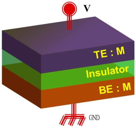
Figure 2.
Metal–insulator–metal (MIM) structure. Reprinted with authorization under a CC BY License from reference []. Copyright 2013 Springer.
Various operation modes need to be executed depending on the type of the memristor. Figure 3a,b schematically depicts characteristic current–voltage (I–V) graphs obtained from DC voltage sweeps. The memristor exhibits two distinct resistance states: low-resistance state (LRS), termed the ON state, and high-resistance state (HRS), termed the OFF state. Additionally, multilevel RS functioning makes use of intermediate resistance states. The process of changing an RS device from HRS to LRS upon applying an external forward bias is known as the SET process. In contrast, applying a reverse bias to the memristor switches it to the HRS state from the LRS state. This process is well defined as the RESET process. However, the memristor devices often require a forming step prior to the SET operation. A voltage greater than the set voltage is applied during the forming process. This triggers a soft dielectric breakdown in the insulator layer, so activating the memristor (Figure 3b).
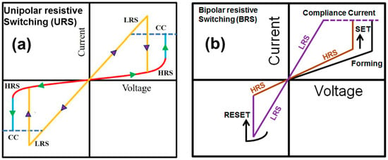
Figure 3.
Schematic of I–V curves obtained from RS device, showing two RS modes: (a) unipolar. Reprinted with authorization under a CC BY License from reference []. Copyright 2022 Elsevier; (b) bipolar.
The memristors are broadly classified as unipolar and bipolar RS devices depending on the mode of their SET/RESET operations. Figure 3 schematically depicts the I–V characteristics of a MIM device for the two switching modes. The RS direction for unipolar RS is determined by the magnitude of the applied voltage, rather than voltage polarity. Therefore, SET and RESET occur at the same polarity. Bipolar switching refers to a phenomenon where the direction of switching is determined by the polarity of the applied voltage. Therefore, SET can only happen when the polarity is in one direction, while RESET can only take place when the polarity is in the counter direction. To prevent the hard breakdown of the memristor, it is necessary to set an appropriate compliance current (CC) in the current measuring devices (e.g., semiconductor parameter analyzers).
The current–voltage characteristics of memristors exhibit either a sharp change in resistance between HRS↔LRS, commonly termed as digital/abrupt switching, or a gradual transition which is termed as analog/gradual switching. The digital and analog types of RS modes are schematically depicted in Figure 4a–d. While digital RS is required for binary nonvolatile memory storage applications, analog RS is attractive for mimicking synaptic applications for neuromorphic computing [].
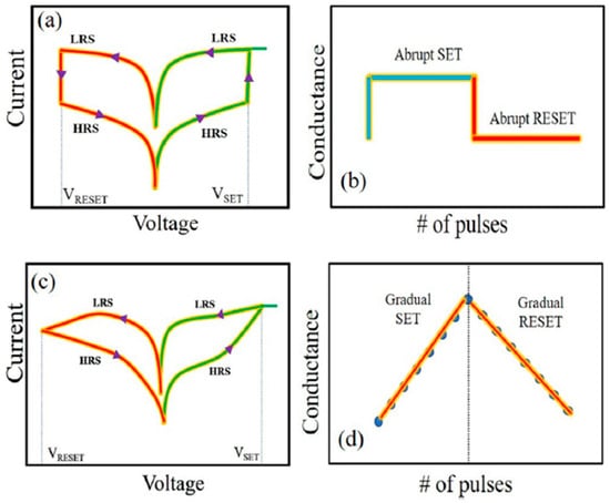
Figure 4.
(a) Digital switching. (b) Abrupt change of conductance for SET and RESET processes. (c) Analog switching. (d) Gradual change of conductance. Reprinted with authorization under a CC BY License from reference []. Copyright 2022 Elsevier.
3. Resistive Switching Mechanism
There are three primary categories of memristors that can be distinguished, which involve migration of ions and coupled redox processes during the RS operations of the MIM device.
The electrochemical metallization (ECM)-based memristors consist of an active metal electrode (Ag or Cu). Set operation in ECM-based memristor cells involves the generation of Ag/Cu ions by electrochemical oxidation, their migration towards the counter electrode, and reduction. This is responsible for the formation of highly conducting metallic filaments connecting both electrodes, which sets the ECM cells to LRS. Upon applying a reverse bias, the filaments undergo electrochemical dissolution, switching the device into the HRS state. To have a comprehensive understanding of ECM, readers are referred to Reference [].
Secondly, the RS based on valence change mechanism (VCM) takes place in a wide spectrum of metal oxides that involves a change of oxidation state of the metal ion due to redox reactions during the operation of the memristive cells. This is associated with the migration of mobile ions. In various metal oxides that exhibit migration of mobile ions, the motion of the corresponding VOs in the switching layer plays a pivotal role in determining their RS properties. Memristors driven by this mechanism are also termed OxRAM devices. For VCM devices, the electrode metals are electrochemically inactive. The physical concept of the switching in VCM-based different metal oxides is based on the push-pull mechanism of the VOs, which leads to the change of resistance of the switching device. As seen in Figure 5, the type of RS can be divided into two types depending on the current conduction mechanisms: (1) filamentary type, (2) interface type.

Figure 5.
Schematic showing VCM mechanisms: (a) filamentary type; and (b) an interface type. Reprinted with authorization under CC BY License from reference []. Copyright 2013 Springer.
Another type of RS mechanism involves the utilization of the thermochemical memory (TCM) effect, also known as fuse-antifuse memory, which occurs when the temperature increases as a result of current flow. To have a comprehensive understanding of TCM, readers are referred to Reference [].
In the present review article, our focus will be on the VCM-type RS in metal oxides, which greatly depends on the movement of VOs present in the oxide matrix of a memristor.
4. Modulation of the Concentration of VOs in Metal Oxides
In a variety of metal oxides, VOs are typical point defects. The physicochemical properties of oxides, including resistance, are tuned precisely by the concentration of VOs. To tune the oxygen non-stoichiometry in metal oxides, a variety of strategies are reported in the literature, such as:
4.1. Doping
Incorporation of aliovalent dopants is a familiar technique to induce VOs in metal oxides. For instance, after doping ZrO2 with divalent Ca2+, where Ca ions substitute zirconium ions sites, VOs are created to maintain the charge neutrality. The defect equation can be expressed as .
Introducing dopants in metal oxides is an effective way to modulate their current conduction properties. In the literature, it had been reported that p-type aliovalent dopants (such as Al) which induce additional holes in a chosen metal oxide (e.g., HfO2) may greatly reduce the defect formation energy []. The formation energy of VOs defects are strongly related to the CF forming process where VOs are created and driven to aggregate by an external applied voltage [].
It has been hypothesized that a decrease in forming voltage may result from a decrease in VOs formation energy []. The formation energies of VOs can also impact the stability of the CF as well as the migration of VOs near dopants, thereby changing the retention and switching performance of RS devices [,]. To test the consequence of doping on the switching properties of a memristor, Jiang et al. [] conducted the first principle calculation on how different aliovalent dopants influence oxygen vacancy formation in Ta2O5. According to their research, p-type dopants can enhance the retention properties, decrease the forming voltage, and set the voltage of Ta2O5-based memristors. Kukli et al. [] investigated the RS characteristics of the Zr-doped Ta2O5 memristor. In this work, Ta2O5 thin films with varying concentrations of ZrO2 were fabricated via atomic layer deposition (ALD) and subsequently subjected to annealing at a temperature of 800 °C in a nitrogen environment for a duration of 10 to 30 min. The observed phenomenon of RS in the Zr-doped Ta2O5 memristor had a distinct pattern where an increase in Zr doping concentration led to a decrease in the forming voltages. Moreover, 30 nm Ta2O5 thin films with minimal Zr doping concentration exhibit a higher forming voltage of 4 V. In contrast, films with similar thickness and doping levels of 0.2 and 0.9 atom % Zr in Ta2O5 exhibit reduced forming voltages of 2.5 and 2.0 eV, respectively. The obtained results are well accord with the theoretical predictions [] that the utilization of p-type dopants can influence the process of electroforming. P-type dopants lower VOs formation energies and can encourage generation of VOs during thermal annealing, which can greatly lower the forming voltage or even enable the fabrication of forming-free devices.
Various methodologies have been successfully used to dope different aliovalent elements in oxide materials to create VOs, such as chemical synthesis route [], chemical vapor deposition (CVD) [], co-sputtering [], hydrothermal synthesis [], ALD [], pulsed laser deposition (PLD) [], and chemical spray pyrolysis [].
4.2. Magnetron Sputtering Technique
One of the most promising physical vapor deposition (PVD) techniques, magnetron sputtering, is thought to provide a pragmatic approach to modulate the stoichiometry of oxides. By controlling the stoichiometry of the oxide layers, we can modulate the oxygen vacancy concentrations. The performance of a memristor device may be greatly impacted by changing the stoichiometry of the sputtered growth oxide thin films. This can be accomplished by modifying the sputtering parameters (e.g., partial pressure of oxygen during the growth of the films, and substrate temperature). Oxygen partial pressure directly affects the stoichiometry of the grown layers. A higher concentration of VOs is produced by lower partial pressure of oxygen, while stoichiometric films with a lower number of VOs in the deposited thin films are produced by higher partial pressure of oxygen. For instance, Q. Cai et al. [] modulated the concentration of VOs in TaOx films by the magnetron sputtering technique. In this experiment, a mixture of argon and oxygen was purged into the sputter chamber. The flow rate of argon was maintained at 20 standard cubic centimeters per minute (SCCM), while oxygen was injected at flow rates of 3 SCCM, 4 SCCM, and 5 SCCM. This modulation resulted in gas mixes with oxygen contents of 13%, 16%, and 20%, respectively. Different percentages of oxygen contents create different concentrations of VOs in the oxide thin films. The number of different VOs has an important impact on the RS properties of an oxide-based memristor, which will be discussed in the next section.
4.3. Thermal Treatment
Thermal treatment is considered as an effective knob to tune VOs in metal oxides under different atmospheres. For example, Pan et al. [] created the VOs in titanium oxide (TiO2−x) by thermal treatment under different gas atmospheres, such as pure argon, nitrogen gas, or in a vacuum system. In their work, Abbas et al. [] modulated the concentration of VOs in ZrOx thin films via the RTA process conducted within the temperature range of 500 °C–800 °C under oxygen ambience.
4.4. Pulsed Laser Deposition (PLD)
PLD is a highly adaptable methodology that is extensively employed for the purpose of fabricating thin films of metal oxides, allowing for precise control over stoichiometry of the thin films. One notable characteristic of PLD is its capacity to generate VOs within the films that are fabricated. The concentration of these vacancies can be precisely regulated by optimizing several PLD parameters, namely, oxygen partial pressure, energy density, laser pulse repetition rate, etc.
4.5. Atomic Layer Deposition (ALD)
ALD, or atomic layer deposition, is a thin-film deposition method that gives exact control over the atomic-level composition and thickness of thin films. Production of oxygen vacancies in materials by ALD requires the implementation of several specific strategies, which vary according to the target material and targeted applications. Optimal selection of the metal precursor in ALD is crucial for precise control of the stoichiometry of the prepared films. Metal halides, alkoxides, and metalorganic compounds are representative examples of common metal precursors. A crucial function is also played by the oxygen precursor, such as H₂O, O3, or oxygen plasma. By modifying the reactivity and amount of the oxygen source, it is possible to produce non-stoichiometric oxide films having a certain amount of VOs depending on the growth parameters. Implementing a plasma source during ALD can expedite the generation of VOs. A plasma with reducing properties, such as H₃ or NH₃ plasma, can be employed to generate or maintain VOs throughout the process of film formation []. Liu et al. [] synthesized the HfOx layers with different VOs concentrations by varying the duration of H2 plasma treatment from 13.5 s to 25.5 s, while maintaining a purge time of precisely 15 s. Deposition of 2 nm stoichiometric HfO2 films was carried out via thermal atomic layer deposition (TALD) at 250 °C, utilizing Hf[N(C2H5)CH3]4 (TEMAH) and H2O precursors. Furthermore, they investigated the impact of VOs concentrations in non-stoichiometric HfOx layers on RS characteristics/synaptic properties (discussed in the following section) of Pt/HfO2/HfOx/TiN memristor.
5. Oxygen Vacancy-Engineered Oxide Thin Films for Memristors
In this part, the state-of-the-art research on the VOs-engineered metal oxide-based memristor and its applications are discussed.
5.1. Memory Storage Applications
Several metal oxides, including transition metal oxides (TMOs), have been explored for their potential deployment in VCM-based memristors. The reliable operation of ReRAMs depends primarily on controlling the VOs concentrations, because the switching process is closely related to movement of VOs and its accumulation inside the oxide layer forming the conducting filament (CF). CF stability in RS devices, particularly under the influence of coulombic repulsive forces, is a critical aspect of their performance and reliability. Once the filament is formed, the coulombic repulsive forces due to the like-charged VOs within the filament can cause the instability. It is well acknowledged that RS results from charged VOs being redistributed upon applying an external bias. Nevertheless, this assumption is counterintuitive to the experimentally observed stable filaments, as the presence of a high concentration of VOs is expected to result in a strong coulombic repulsion and subsequent instability of the filament []. The advancement of an atomistic representation that can effectively elucidate the internal dynamics of RS in oxide-based RRAM is of the utmost importance in enhancing comprehension of RS processes and providing guidance for device optimization and applications. Lee et al. [] investigated the interactions between different charged VOs in an amorphous Ta2O5-based RS device implementing first-principles calculations. A strong repulsive interaction was observed between charged vacancies, whereas neutral vacancies exhibited short-range attraction. Drawing upon theoretical predictions, a model was presented, comprising a sequence of charge transition events, that effectively elucidates the phenomenon of vacancy drift and aggregation throughout the process of RS. The proposed model effectively integrates experimental findings, such as the phenomenon of field-driven ionic transport and the creation of stable filaments under conditions of high VOs concentration. Hence, it is very crucial to modulate the VOs concentrations meticulously in oxide thin films via different strategies, such as bilayer engineering, interface engineering, tuning the growth parameters, doping, etc. to achieve optimized device performances.
Sharath et al. [] reported the forming-free RS in VOs-engineered hafnium oxide thin films. In their work, nonvolatile RS behavior was investigated in VOs-engineered HfO2−x layers grown by the molecular beam epitaxy (MBE) technique. Concentration of VOs were tuned by the oxygen partial pressure during thin-film growth. It was observed that the electroforming voltage was significantly reduced as compared to stoichiometric hafnium oxide thin films.
The most propitious memristors, which depend on the Ta2O5 layer’s RS, stands out especially when they include a non-stoichiometric TaOx layer. The reduction in the forming voltage was observed on reactive-sputtered grown oxygen-deficient Ta2Ox films by Skaja et al. []. This was discussed in the framework of the thin-film deposition parameter-dependent microstructure, nature of the electrodes, and VOs concentration inside the oxide matrix. Sharath et al. [] demonstrated RS properties of TaOx-based bilayer thin films with engineered VOs grown by the MBE technique. The XPS analysis revealed the presence of all possible valence states of Ta, including metallic Ta, in non-stoichiometric TaOx films. It was demonstrated that with increasing VOs in TaOx formation, the voltage reduced from 10.5 V to 1.5 V. In contrast, it was observed that, irrespective of oxygen content, there was a stable bipolar RS in all devices. Furthermore, it was observed that unipolar switching may coexist with bipolar RS only at higher oxygen contents, which transforms to a threshold switching behavior under conditions of highest oxidation. The observed phenomenon of unipolar RS can be attributed to the significant influence of Joule heating during the switching process. The primary mechanisms involved in the SET and RESET processes are believed to be the clustering of VOs facilitated by a temperature gradient and the thermal diffusion of vacancies produced by a concentration gradient []. It has been reported that the thermal conductivity of TaOx films exhibits an upward trend as the level of VOs increases []. Hence, it can be inferred that the unipolar RS in oxygen-deficient thin films is hindered by a reduced concentration gradient and increased heat dissipation. In films with the highest level of oxidation, the local Joule heating reaches its maximum value. Consequently, if there is an inadequate dissipation of heat, it leads to a changeover from unipolar to threshold-resistive switching [].
In another work, Egorov et al. [] investigated the RS characteristics in oxygen vacancy-engineered TaOx film. The film was grown via the PEALD technique, with Ta(OC2H5)5 reactant and plasma-activated hydrogen as a precursor to modulate the concentration of VOs. The TaOx layer, which lacked oxygen, worked as the source of VOs for the RS of the Ta2O5 layer. Although the beneficial effects of the VOs-modulated TaOx layer had been previously documented when grown via reactive sputtering, the growth of an oxygen-deficient layer by the ALD technique and its subsequent performance verification represent a significant advancement in integrating RS devices with well-established industry deposition techniques. Prakash et al. [] demonstrated improved RS properties of the TaOx layer by introducing a TiOx in the W/TaOx/W memristors (DC sweep characteristics are shown in Figure 6). The W/TiOx/TaOx/W memristors exhibit 104 consecutive DC sweep cycles, endurance of >105 cycles (shown in Figure 7a), and retention of >104 s (shown in Figure 7b) with a switching window of >102 at 85 °C. Furthermore, the fabricated memristor can function at a lower compliance current of 23 μA. The Auger electron spectroscopy confirmed the existence of VOs-based TaOx nanofilaments after switching operation of the device. The movement of oxygen ions was found to be responsible for filament formation, as well as dissolution of the filament, and it was regulated by a thin Ti layer located at the electrode/oxide interface.
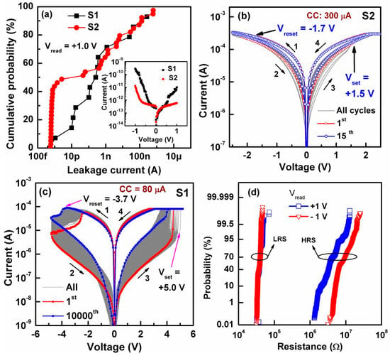
Figure 6.
RS characteristics of Ti layer-inserted TaOx−based (device S1) and standalone TaOx-based memristors (device S2). Reproduced with authorization under CC BY License from reference []. Copyright 2014 Springer. (a) Cumulative probability of leakage currents for S1 and S2 devices with typical via size of 0.8 μm. Inset: leakage current vs. voltage characteristics. Switching I-V curves of (b) S2 and (c) S1 devices. The S2 device shows instability after a few cycles, while 10,000 consecutive switching cycles are observed for the S1 device. (d) Cumulative probability of LRS and HRS under Vread of ±1 V for the S1 devices.
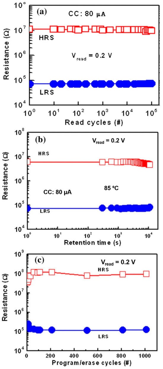
Figure 7.
(a) Pulse endurance. (b) Memory state retention showing memory window of >102. (c) Program/erase endurance cycles. Reproduced with authorization under CC BY License from reference []. Copyright 2014 Springer.
Rudrapal et al. [,] reported forming-free bipolar RS, self-compliance, and multilevel RS in oxygen vacancy-modulated WO3−x-based memristors. In this work, concentration of VOs was modulated by varying the partial pressure of oxygen during the reactive sputter growth of WO3−x thin films. The concentration of VOs was varied between ~ 1 × 1021 cm−3 to ~ 9 × 1020 cm−3. Figure 8b–f represents the RS memory characteristics of the VOs-engineered WO3−x samples. It is worth noting that the samples with a concentration of VOs in the range of approximately 1 × 1021 cm−3–6.2 × 1020 cm−3 demonstrated consistent and reliable bipolar switching without the need for any extra electroforming process. The forming-free behavior of the memristor can be due to the higher [VOs] in the WO3−x thin films. Furthermore, a sample with VOs concentration ~ 6.2 × 1020 cm−3 exhibited excellent stability in a bipolar RS mode with a set and reset voltage of −2 V and 3 V, respectively; window margin of 2 × 10³, stable endurance (~6000 cycles), and a retention time of ~8 × 10³ s. Increasing the oxygen content in the WO3-x layer required an extra forming step before demonstrating resistive switching for the sample with [VOs] ~5.8 × 1020 cm−3 (as seen in Figure 8e). Further lowering of VOs concentration to ~4.5 × 1020 cm−3 renders the WO3−x film’s highly insulating nature. The resistance W/WO3−x/Pt memristors with a highly insulating WO3−x layer were non-switchable to LRS despite applying a higher DC voltage of −10 V (as shown in Figure 8f. The correlation between the concentration of VOs and systematic changeover from forming-free resistive switching to forming-required resistive switching and, finally, non-formable devices, strongly indicates a deterministic role of precise VOs engineering in the WO3−x thin films in tuning their resistive switching properties for device applications.
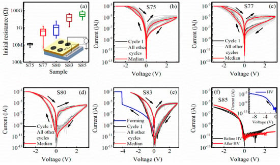
Figure 8.
(a) Initial resistance of all pristine devices. (b–e) I–V responses of the samples having different concentration of VOs. (f) DC sweep cycles for highly insulating WO3–x layer, which is non-switchable, inset represents the applied high-voltage (HV) step. Reprinted with permission from reference []. Copyright 2022 Wiley-VCH GmbH.
In another work, Ghenzi et al. [] reported electroforming-free RS in TiO2-based memristor devices by controlling the partial pressure of gas during the growth of oxide layer, which tunes the oxygen vacancy concentration. In such instances, it is assumed that increased oxygen vacancy concentration promotes the formation of a low-resistance channel in the oxide matrix, which lowers the forming voltage as well as improving the other RS characteristics.
As mentioned earlier, incorporation of various dopants into metal oxides have been attempted to tune the VOs. Hong et al. [] explored the effect of an aliovalent Nb dopant on the voltage stability of ZnO-based memristor. Nb-doped ZnO (NbxZn1−xO, NZO) thin films were grown on platinized Si (Pt-Si) substrates using the RF sputtering technique. The concentration of Nb doping was seen to impact the microstructure and the quantity of VOs. Among the various doped samples, the NZO film with an Nb doping concentration of 0.5 at% demonstrated a stable set/reset voltage (i.e., optimal coefficients of variation (Cv) of 7.02% for reset operations and 2.73% for set operations). It also showed a decent endurance, stable up to ~1000 cycles. Additionally, the device had lower set and reset voltages of 1.83 V and 0.57 V, respectively, owing to a higher concentration of VOs in the NZO switching layer.
Table 1 presents a comparative analysis of the Vreset, Vset, and Cv values of the 0.5 at% Pt/NZO/Pt film in relation to various other metal-doped ZnO memristors reported by different research groups. The observed performance of the NZO in terms of Vreset and Vset is comparable to that of pure ZnO; however, Cv exhibits a notable improvement. Furthermore, in comparison to the ZnO:Ti sample, NZO exhibits superior properties in all aspects. Moreover, the NZO memristor exhibits superior properties compared to the V-doped ZnO and Zr-doped ZnO. Overall, the findings indicate that VOs-modulated NZO thin films have potential as reliable and energy-efficient materials for memory storage applications as compared to other metal-doped ZnO memristors.

Table 1.
Comparison of reset voltage, set voltage, and Cv for various metal-doped ZnO memristors.
Sedghi et al. [] executed an experiment to test the impact of non-metal (nitrogen) doping on Ta2O5-based memristors and their RS properties. From the experimental findings it was inferred that introduction of nitrogen improves memory state retention properties, as it counteracts the presence of electronic defects linked to VOs. In addition, the introduction of nitrogen doping increases the switching window to accommodate a greater number of intermediate states. This enhancement improves the stability of resistive switching (RS) and also allows for a gradual reset function. In addition, devices made of N-doped Ta2O5 exhibit low set and reset voltages (<1 V) with decreased variability. Table 2 represents performance parameters of several VOs-engineered RS memristors.

Table 2.
VOs-engineered RS memristors and their corresponding performance parameters.
5.2. Neuromorphic Applications
The two basic building blocks of the computational system in the brain are neurons and synapses. The biological synapse is a small gap at the end of a neuron where the signal is transferred from one neuron to another neuron. It is a crucial component of information transfer. Synaptic plasticity refers to the ability to modify the signal-integrating function of biological synapses by adjusting the synaptic weight, the connection strength between pre-synapse and post-synapse []. Short-term plasticity and long-term plasticity are distinct types of synaptic plasticity. Short-term plasticity is the phenomenon of synaptic transmission efficiency fluctuating over a brief period of time. It can lead to short-term potentiation (STP); for example, paired-pulse facilitation (PPF), or short-term depression (STD), and excitatory postsynaptic current (EPSC). Conversely, long-term potentiation (LTP) denotes a durable augmentation in the effectiveness of synaptic communication over an extended duration. It is accomplished by the activity patterns that occur between neurons located before and after the synapse. Spike timing-dependent plasticity (STDP) and spike rate-dependent plasticity (SRDP) are dominant mechanisms that regulate the capacity of synapses to modify their strength. STDP primarily considers the temporal sequence of activity between the pre-synapse and post-synapse, whereas SRDP places more importance on the frequency of activity in the presynaptic neurons []. Currently, various neuromorphic devices have been used to replicate a wide range of synaptic plasticity. These devices can change their conductivities, enabling a transition between several resistance states and demonstrating either volatility or non-volatility. This mimics the properties of artificial synapses’ LTP or short-term potentiation (STP).
The memristor exhibits a mimicked RS behavior that necessitates gradual set and reset processes instead of abrupt ones in order to simulate biological synapses. Recently, various research groups have reported the different synaptic functions in oxygen vacancy-engineered oxide thin films. The CMOS compatibility and straightforward MIM structure of the metal oxide-based electronics synapse make it a viable option for neuromorphic applications in the future. Synaptic devices based on Ta2O5, TiOx, WOx, HfOx, AlOx, and TiOx/TaOx multilayers have been reported. Abbas et al. [] designed an oxygen-deficient tantalum oxide-based neuromorphic device which exhibited the abrupt HRS to LRS transition and gradual LRS to HRS transition. The properties of abrupt set and gradual reset processes are due to the migration of VOs and gradual alteration of the filament’s structure. In the Ti/Ta2O3−x/Pt memristor, the Ti electrode on top was designated as the presynaptic input terminal and the bottom Pt electrode was fixed as the postsynaptic output terminal.
Tantalum oxide thin-film composition has been studied using X-ray photoelectron spectroscopy (XPS) (as shown in Figure 9a,b). The physical characteristics of a tantalum oxide-based synaptic device were inspected using transmission electron microscopy (TEM) and energy-dispersive X-ray spectroscopy (EDX) analysis. Cross-sectional scanning (as provided in Figure 10) of the fabricated device was achieved by scanning TEM (STEM) high-angle annular dark field (HAADF). Figure 10d displays the vertical distribution of element intensities throughout the sample. Oxygen concentration profiles demonstrated that oxygen was present at the interface, which is related to the formation of TiOy there. Therefore, the Ti and Ta2O3−x interface was considered as the reservoir of VOs. In another work, Zongwei et al. [] developed a TaOx-based memristor by incorporating a SiO2 thin film between the TiN and TaOx interface. This SiO2 layer acts as a barrier layer and controls the concentration of filament-forming species, e.g., VOs/ions that take part in switching. This study demonstrates that the variation in defect concentration between the electrode and dielectric interface is crucial in enabling the memristor to exhibit analog switching or function as a neuromorphic device.
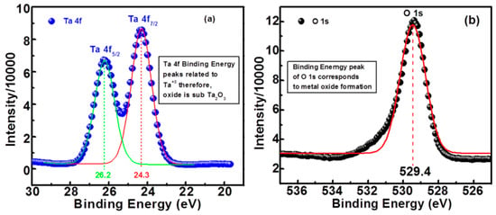
Figure 9.
XPS spectrum of tantalum oxide thin films. (a) Ta 4f and (b) O 1s. Reproduced with authorization CC BY License from reference []. Copyright 2018 Nature.


Figure 10.
(a) STEM HAADF micrograph of Ta2O3−x−based RRAM device. (b) STEM bright field image. Red squares represent the amorphousness of Ta2O3−x and crystalline Pt. (c) EDX profiles of Ti/Ta2O3−x/Pt. (d) Separate line profiles showing the characteristics of each element of the device along the vertical direction. Reproduced with authorization under CC BY License from reference []. Copyright 2018 Nature.
Gao et al. [] demonstrated the synaptic behavior in the HfO2-based RS device. The device structure is given in Figure 11.
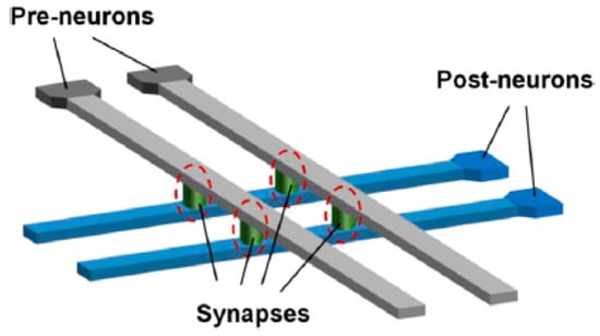
Figure 11.
Schematic illustration of a memristive synapse. Structure consists of using TiN (pre-neuron)/Gd:HfOx/Pt (post-neuron) memristive devices. Reproduced with authorization under CC BY License from reference []. Copyright 2015 Elsevier.
A Gd-doped HfO2 synaptic device has demonstrated encouraging synaptic properties, including low learning–forgetting energy consumption and controllable multilevel ability. Figure 12 shows the memory function of the TiN/Gd:HfOx/Pt. As shown in Figure 12a,b, analog-type transition was recorded and resistance of the synaptic device decreased with the cumulative pulse time. Initially, the resistance was not affected by the increasing number of pulses. This phenomenon can be linked to the stochastic character of the formation of VOs []. Furthermore, under varied pulse settings, the synaptic device’s potentiation and depression features were demonstrated.
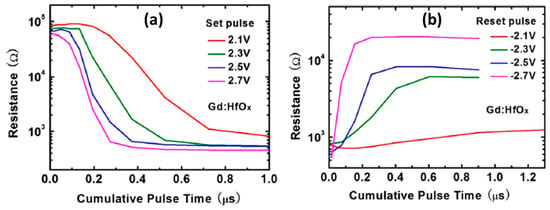
Figure 12.
Resistance–cumulative pulse time response for Gd−doped HfOx synaptic device: (a) set and (b) reset processes. Reproduced with authorization under a CC BY License from reference []. Copyright 2015 Elsevier.
Liu et al. [] investigated the synaptic function of the HfO2/HfOx ultrathin bi-layered memristive devices, specifically focusing on the HfOx layer with an optimal oxygen vacancy content of 12.1%. An array of crucial synaptic functions were achieved in a bilayer-based ultrathin memristive device, including non-linear synaptic characteristics, PPF, and STDP (as represented in Figure 13). The changeover from STP to LTP adheres to the Ebbinghaus forgetting curve, emulating memory patterns of the brain. The device was equipped with an extremely thin functional layer of HfOx/HfO2, measuring approximately 6 nm in thickness. This resulted in a significantly faster switching speed, taking less than 10 nanoseconds. The energy usage per operation was assessed to be approximately ten-picojoules. Based on these findings, it is evident that oxygen vacancy-engineered HfOx-based memristors show great potential for effective utilization of synapses for neuromorphic applications.


Figure 13.
(a) Change in the current response of the HfOx-based bilayer memristor due to successive potentiation or depression pulses. (b) STDP features. The synaptic weights (ΔW) vary in relation to the spike times (Δt). (c) PPF index upon applying negative voltage pulse. (d) PPF index upon applying positive voltage pulse. (e) STP to LTP transition. The synaptic weight decay curve measured following 10, 30, 50, 70, 90, and 110 consecutive pulses. (f) Change in relaxation time (τ). Reprinted with permission from reference []. Copyright 2020 Royal Society of Chemistry.
Furthermore, Rudrapal et al. [] demonstrated the synaptic characteristics of a VOs-rich WO3−x-based MIM device. The observed gradual increment in current during the voltage sweep in WO3−x films indicates the presence of gradual-type RS with synaptic plasticity. This phenomenon had been identified using voltage biases lower than the set voltage during I–V cycling test.
Figure 14a,b demonstrate the analog switching characteristics of an oxygen vacancy-rich WO3−x memristor with a voltage bias of –1.8 V and +1.8 V, respectively, for five successive DC sweep cycles. Upon applying the voltage in the negative direction, the resistance of the WO3−x memristor gradually decreased (as given in Figure 14a) direction for several cycles. Incremental increase or decrease in conductance over time when applying the DC voltage sweep in oxygen vacancy-engineered samples can be considered as a reliable representation of synaptic properties. In another work, Mohapatra et al. [] demonstrated not only the analog bipolar RS but also the neuromorphic learning and recognition in the oxygen vacancy-rich WO3−x memristor. The fabricated memristor exhibited several resistance states and has great potential for emulating synaptic functions. In this work, multiple cycles of potentiation and depression were demonstrated at ±1.8 V and ±2 V. Through this experimental approach, the device’s capacity to maintain synaptic function over time is validated, and its adaptability to varying voltage levels is highlighted. Furthermore, the Modified National Institute of Standards and Technology (MNIST) pattern recognition accuracy of the W/WO3−x/Pt memristor was calculated by using the output current as the weight of the synapse. The image recognition capabilities of the synaptic devices were evaluated by using a multilayer feed-forward Neural Network (NN) architecture with one hidden layer, as shown in Figure 15a. A validation accuracy of ~95 % was achieved for the WO3−x memristor (Figure 15b). This indicates that oxygen vacancy-engineered WO3−x-based memristors are suitable for mimicking the biological synapse in neuromorphic computing applications.
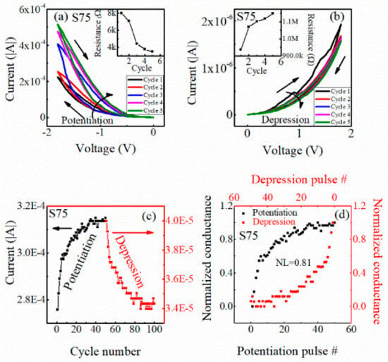
Figure 14.
Synaptic characteristics of oxygen vacancy-rich WO3−x memristor. Series of sequential DC cycles (a) potentiation, as indicated by a drop−in resistance; and (b) depression, as indicated by an increase in resistance. (c) 50 successive pulse cycles to induce potentiation and depression. (d) Modulation of normalized conductance with the application of pulse sequences. Reprinted with permission from reference []. Copyright 2023 IOP Publishing Ltd.
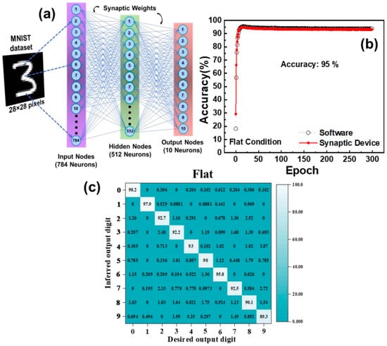
Figure 15.
(a) Diagrammatic depiction of an Artificial Neural Network (ANN) with three layers: input, hidden, and output. (b) The percentage of recognition accuracy for MNIST handwritten digits is computed for both the software-based ideal numeric scenario and the suggested WO3−x-based synaptic device, with respect to the number of epochs conducted. (c) The confusion matrix of testing data for the synaptic device. Reprinted with permission from reference []. Copyright 2024 IOP Publishing Ltd.
Despite the promising advancements so far, the memristive neuromorphic system remains in its nascent phase, and numerous challenges persist that want thorough attention and resolution. The difficulties associated with existing neuromorphic devices mostly originate from the inherent nonidealities of memristors, including the drift and nonlinearity of conductance evolution, and device-to-device variation. The drift and nonlinearity of conductance provide a significant challenge to achieve artificial synaptic weight modulation, hence directly affecting the learning efficacy of memristive neural systems. Spatial and temporal variations in memristive neuromorphic devices are potential obstacles which need to be solved for real-world applications. The spatial variation is responsible for different electrical characteristics, while temporal variation leads to stochasticity. Such device-to-device and cycle-to-cycle to stochasticity have a direct impact on the data stored in memristive devices.
6. Summary and Future Perspectives
In this review, we covered materials used in the development of memristors, such as WO3, ZnO, HfO2, Ta2O5, TiO2, etc. We also delved into the functionality of memristors in detail. We examined the design of the oxygen vacancy-engineered oxide layer that influences the performance of these devices. The review showcased cutting-edge achievements in memristor research. Furthermore, we discussed the applications of memristors in storage class memory and neuromorphic computation. After decades of research, memristor technology has made advancements; however, there are still several obstacles to overcome before its commercialization becomes feasible. Various research groups may propose various RS mechanisms for the same sandwich structure material, which can be attributed to variations in the production method.
Several aspects of the memristor device primarily impact the reliability of systems based on memristors. The three main issues with memristor device reliability are endurance, retention, and variability []. The variability of the memristive device is largely determined by the CFs composed of VOs. These filaments exhibit variations based on numerous physical factors, including layer thickness, doping concentrations, and operating conditions [,]. This fluctuation or non-uniformity poses a major obstacle in the production of memristor devices.
Retention is an important parameter of memristors since it enables the stored data to persist over time. For nonvolatile memories, the anticipated duration of data retention exceeds 10 years. These capabilities of memristors have been described in detail in recently published papers []. Nevertheless, it is crucial to acknowledge that factors such as write speed and read voltage stress can affect these characteristics. To achieve optimal device retention, it is essential to consider the magnitude of the voltage applied to the memristor during the read operation [].
Further investigation is required in the future to demonstrate the atomistic mechanism of RS more systematically. Most RS materials are not suitable for CMOS technologies; this limitation restricts their practical applicability. Hence, the integration method must be capable of accommodating both standard CMOS-friendly and CMOS-incompatible materials to ensure broader future applications.
The potentiation and depression linearity, power consumption, and spatial and temporal variations of memristors have been found to be suboptimal, requiring further enhancement of device performances. Moreover, the human sensory system is a confluence of various senses. Hence, the development of device systems that incorporate multisensory fusion and various processing abilities has tremendous promise for further applications. In the future, it is necessary to further develop brain-like applications utilizing memristors.
There is still a sizable difference between the memristive and biological nervous systems, and the main obstacle is the lack of neural circuits, including artificial synapses and neurons. The predominant neural models now employed in the memristive nervous system are uniform and deficient in biological details, in contrast to the wide range of variation found in biological nervous systems. Hence, the absence of dedicated functional specialization in neural models hinders the memristive nervous system from efficiently processing information in comparison with the brain []. Given that memristors have intrinsic bio-realistic qualities, considerable work should go into simulating neural circuits that can precisely replicate biological activities at low to no additional expense. Therefore, the memristive nervous system would be more comparable to the organic nervous system in terms of its capabilities.
Author Contributions
Conceptualization, review, and editing by A.R.C.; original manuscript preparation, review, and editing by B.J. All authors have read and agreed to the published version of the manuscript.
Funding
This work is partially funded by SERB (CRG/2021/000811).
Conflicts of Interest
The authors declare no conflict of interest.
References
- Chua, L. Memristor-the missing circuit element. IEEE Trans. Circuit Theory 1971, 18, 507–519. [Google Scholar] [CrossRef]
- Chua, L. Everything you wish to know about memristors but are afraid to ask. In Handbook of Memristor Networks; Springer: Cham, Switzerland, 2019; pp. 89–157. [Google Scholar]
- Xiao, Y.; Jiang, B.; Zhang, Z.; Ke, S.; Jin, Y.; Wen, X. A review of memristor: Material and structure design, device performance, applications and prospects. Sci. Technol. Adv. Mater. 2023, 24, 2162323. [Google Scholar] [CrossRef] [PubMed]
- Hickmott, T.W. Low-frequency negative resistance in thin anodic oxide films. J. Appl. Phys. 1962, 33, 2669–2682. [Google Scholar] [CrossRef]
- Liu, S.; Wu, N.J.; Ignatiev, A. Electric-pulse-induced reversible resistance change effect in magnetoresistive films. Appl. Phys. Lett. 2000, 76, 2749–2751. [Google Scholar] [CrossRef]
- Lee, M.-J.; Park, Y.; Kang, B.-S.; Ahn, S.-E.; Lee, C.; Kim, K.; Xianyu, W.; Stefanovich, G.; Lee, J.-H.; Chung, S.-J. 2-stack 1D-1R cross-point structure with oxide diodes as switch elements for high density resistance RAM applications. In Proceedings of the 2007 IEEE International Electron Devices Meeting, Washington, DC, USA, 10–12 December 2007; pp. 771–774. [Google Scholar]
- Strukov, D.B.; Snider, G.S.; Stewart, D.R.; Williams, R.S. The missing memristor found. Nature 2008, 453, 80–83. [Google Scholar] [CrossRef]
- Chevallier, C.J.; Siau, C.H.; Lim, S.F.; Namala, S.R.; Matsuoka, M.; Bateman, B.L.; Rinerson, D. A 0.13 µm 64 Mb multi-layered conductive metal-oxide memory. In Proceedings of the 2010 IEEE International Solid-State Circuits Conference, San Francisco, CA, USA, 7–11 February 2010; pp. 260–261. [Google Scholar]
- Liu, T.-Y.; Yan, T.H.; Scheuerlein, R.; Chen, Y.; Lee, J.K.; Balakrishnan, G.; Yee, G.; Zhang, H.; Yap, A.; Ouyang, J. A 130.7 mm 2 2-layer 32 Gb ReRAM memory device in 24 nm technology. In Proceedings of the 2013 IEEE International Solid-State Circuits Conference Digest of Technical Papers, San Francisco, CA, USA, 17–21 February 2013. [Google Scholar]
- Fackenthal, R. A 16 GB ReRAM with 200 MB/s write and 1 GB/s read in 27 nm Technology. In Proceedings of the 2014 IEEE International Solid-State Circuits Conference Digest of Technical Papers (ISSCC), San Francisco, CA, USA, 9–13 February 2014. [Google Scholar]
- Luo, Q.; Xu, X.; Liu, H.; Lv, H.; Gong, T.; Long, S.; Liu, Q.; Sun, H.; Banerjee, W.; Li, L. Super non-linear RRAM with ultra-low power for 3D vertical nano-crossbar arrays. Nanoscale 2016, 8, 15629–15636. [Google Scholar] [CrossRef]
- Clarke, P. TSMC Offers 22 nm RRAM, Taking MRAM on to 16 nm. Available online: https://www.eenewseurope.com/en/tsmc-offers-22nm-rram-taking-mram-on-to-16nm/ (accessed on 25 August 2020).
- Nano, W. Weebit Nano Taped-Out Its First 22 nm Demo RRAM Chip. Available online: https://www.rram-info.com/weebit-nano-taped-out-its-first-22-nm-demo-rram-chip (accessed on 5 January 2023).
- Wang, C.; Shi, G.; Qiao, F.; Lin, R.; Wu, S.; Hu, Z. Research progress in architecture and application of RRAM with computing-in-memory. Nanoscale Adv. 2023, 5, 1559–1573. [Google Scholar] [CrossRef]
- Gao, B.; Wu, H.; Wu, W.; Wang, X.; Yao, P.; Xi, Y.; Zhang, W.; Deng, N.; Huang, P.; Liu, X. Modeling disorder effect of the oxygen vacancy distribution in filamentary analog RRAM for neuromorphic computing. In Proceedings of the 2017 IEEE International Electron Devices Meeting (IEDM), San Francisco, CA, USA, 2–6 December 2017; p. 4. [Google Scholar]
- Banerjee, W.; Liu, Q.; Hwang, H. Engineering of defects in resistive random access memory devices. J. Appl. Phys. 2020, 127, 051101. [Google Scholar] [CrossRef]
- Prakash, A.; Jana, D.; Maikap, S. TaOx-based resistive switching memories: Prospective and challenges. Nanoscale Res. Lett. 2013, 8, 418. [Google Scholar] [CrossRef]
- Asif, M.; Kumar, A. Resistive switching in emerging materials and their characteristics for neuromorphic computing. Mater. Today Electron. 2022, 1, 100004. [Google Scholar] [CrossRef]
- Lashkare, S.; Uddin, W.; Priyadarshi, K.; Ganguly, U. Emerging Memory Technologies for Data Storage and Brain—Inspired Computation: A Global View with Indian Research Insights with a Focus on Resistive Memories. Proc. Natl. Acad. Sci. India Sect. A Phys. Sci. 2023, 93, 459–476. [Google Scholar] [CrossRef]
- Kozicki, M.N.; Mitkova, M.; Valov, I. Electrochemical metallization memories. In Resistive Switching: From Fundamentals of Nanoionic Redox Processes to Memristive Device Applications; Wiley: Weinheim, Germany, 2016; pp. 483–514. [Google Scholar]
- Ielmini, D.; Bruchhaus, R.; Waser, R. Thermochemical resistive switching: Materials, mechanisms, and scaling projections. Phase Transit. 2011, 84, 570–602. [Google Scholar] [CrossRef]
- Zhao, L.; Ryu, S.-W.; Hazeghi, A.; Duncan, D.; Magyari-Köpe, B.; Nishi, Y. Dopant selection rules for extrinsic tunability of HfO x RRAM characteristics: A systematic study. In Proceedings of the 2013 Symposium on VLSI Technology, Kyoto, Japan, 11–13 June 2013; pp. T106–T107. [Google Scholar]
- Yang, Y.; Lu, W.D. Progress in the characterizations and understanding of conducting filaments in resistive switching devices. IEEE Trans. Nanotechnol. 2016, 15, 465–472. [Google Scholar] [CrossRef]
- Jiang, H.; Stewart, D.A. Enhanced oxygen vacancy diffusion in Ta2O5 resistive memory devices due to infinitely adaptive crystal structure. J. Appl. Phys. 2016, 119, 134502. [Google Scholar] [CrossRef]
- Lee, J.; Schell, W.; Zhu, X.; Kioupakis, E.; Lu, W.D. Charge Transition of Oxygen Vacancies during Resistive Switching in Oxide-Based RRAM. ACS Appl. Mater. Interfaces 2019, 11, 11579–11586. [Google Scholar] [CrossRef] [PubMed]
- Jiang, H.; Stewart, D.A. Using dopants to tune oxygen vacancy formation in transition metal oxide resistive memory. ACS Appl. Mater. Interfaces 2017, 9, 16296–16304. [Google Scholar] [CrossRef] [PubMed]
- Kukli, K.; Kemell, M.; Vehkamäki, M.; Heikkilä, M.J.; Mizohata, K.; Kalam, K.; Ritala, M.; Leskelä, M.; Kundrata, I.; Fröhlich, K. Atomic layer deposition and properties of mixed Ta2O5 and ZrO2 films. AIP Adv. 2017, 7, 025001. [Google Scholar] [CrossRef]
- Zhu, X.; Zhuge, F.; Li, M.; Yin, K.; Liu, Y.; Zuo, Z.; Chen, B.; Li, R.-W. Microstructure dependence of leakage and resistive switching behaviours in Ce-doped BiFeO3 thin films. J. Phys. D Appl. Phys. 2011, 44, 415104. [Google Scholar] [CrossRef]
- Lei, M.; He, H.; Yu, Q.; Chen, C.; Lu, Y.; Ye, Z. Optical properties of Na-doped ZnO nanorods grown by metalorganic chemical vapor deposition. Mater. Lett. 2015, 160, 547–549. [Google Scholar] [CrossRef]
- Chang, T.-J.; Li, C.-Y.; Chu, S.-Y. Ta2O5 doping effects on the property improvement of HfOx-based RRAMs using co-sputtering deposition method. Mater. Charact. 2023, 199, 112786. [Google Scholar] [CrossRef]
- Zhang, P.; Gao, C.; Lv, F.; Wei, Y.; Dong, C.; Jia, C.; Liu, Q.; Xue, D. Hydrothermal epitaxial growth and nonvolatile bipolar resistive switching behavior of LaFeO3-PbTiO3 films on Nb: SrTiO3 (001) substrate. Appl. Phys. Lett. 2014, 105, 15. [Google Scholar]
- Henning, R.A.; Leichtweiss, T.; Dorow-Gerspach, D.; Schmidt, R.; Wolff, N.; Schürmann, U.; Decker, Y.; Kienle, L.; Wuttig, M.; Janek, J. Phase formation and stability in TiOx and ZrOx thin films: Extremely sub-stoichiometric functional oxides for electrical and TCO applications. Z. Krist. Mater. 2017, 232, 161–183. [Google Scholar]
- Mundle, R.; Carvajal, C.; Pradhan, A.K. ZnO/Al: ZnO transparent resistive switching devices grown by atomic layer deposition for memristor applications. Langmuir 2016, 32, 4983–4995. [Google Scholar] [CrossRef] [PubMed]
- Deepa, S.; Kumari, K.P.; Thomas, B. Contribution of oxygen-vacancy defect-types in enhanced CO2 sensing of nanoparticulate Zn-doped SnO2 films. Ceram. Int. 2017, 43, 17128–17141. [Google Scholar] [CrossRef]
- Cai, Q.; Duan, Z.; Chen, J.; Wang, X.; Zhu, W.; Liu, S.; Xiao, P.; Yu, X. Tristable TaOx-based memristor by controlling oxygen vacancy transportion based on valence transition mechanism. Ceram. Int. 2024, in press. [Google Scholar] [CrossRef]
- Pan, X.; Yang, M.-Q.; Fu, X.; Zhang, N.; Xu, Y.-J. Defective TiO2 with oxygen vacancies: Synthesis, properties and photocatalytic applications. Nanoscale 2013, 5, 3601–3614. [Google Scholar] [CrossRef]
- Abbas, Y.; Han, I.S.; Sokolov, A.S.; Jeon, Y.R.; Choi, C. Rapid thermal annealing on the atomic layer-deposited zirconia thin film to enhance resistive switching characteristics. J. Mater. Sci. Mater. Electron. 2020, 31, 903–909. [Google Scholar] [CrossRef]
- Liu, C.; Zhang, C.-C.; Cao, Y.-Q.; Wu, D.; Wang, P.; Li, A.-D. Optimization of oxygen vacancy concentration in HfO2/HfOx bilayer-structured ultrathin memristors by atomic layer deposition and their biological synaptic behavior. J. Mater. Chem. C 2020, 8, 12478–12484. [Google Scholar] [CrossRef]
- Sharath, S.U.; Bertaud, T.; Kurian, J.; Hildebrandt, E.; Walczyk, C.; Calka, P.; Zaumseil, P.; Sowinska, M.; Walczyk, D.; Gloskovskii, A.; et al. Towards forming-free resistive switching in oxygen engineered HfO2−x. Appl. Phys. Lett. 2014, 104, 063502. [Google Scholar] [CrossRef]
- Stevens, J.E.; Lohn, A.J.; Decker, S.A.; Doyle, B.L.; Mickel, P.R.; Marinella, M.J. Reactive sputtering of substoichiometric Ta2Ox for resistive memory applications. J. Vac. Sci. Technol. A Vac. Surf. Film. 2014, 32, 021501. [Google Scholar] [CrossRef]
- Sharath, S.U.; Joseph, M.J.; Vogel, S.; Hildebrandt, E.; Komissinskiy, P.; Kurian, J.; Schröder, T.; Alff, L. Impact of oxygen stoichiometry on electroforming and multiple switching modes in TiN/TaOx/Pt based ReRAM. Appl. Phys. Lett. 2016, 109, 173503. [Google Scholar] [CrossRef]
- Yang, J.J.; Strukov, D.B.; Stewart, D.R. Memristive devices for computing. Nat. Nanotechnol. 2013, 8, 13–24. [Google Scholar] [CrossRef]
- Landon, C.D.; Wilke, R.H.T.; Brumbach, M.T.; Brennecka, G.L.; Blea-Kirby, M.; Ihlefeld, J.F.; Marinella, M.J.; Beechem, T.E. Thermal transport in tantalum oxide films for memristive applications. Appl. Phys. Lett. 2015, 107, 023108. [Google Scholar] [CrossRef]
- Egorov, K.V.; Kuzmichev, D.S.; Chizhov, P.S.; Lebedinskii, Y.Y.; Hwang, C.S.; Markeev, A.M. In situ control of oxygen vacancies in TaO x thin films via plasma-enhanced atomic layer deposition for resistive switching memory applications. ACS Appl. Mater. Interfaces 2017, 9, 13286–13292. [Google Scholar] [CrossRef] [PubMed]
- Prakash, A.; Maikap, S.; Chiu, H.C.; Tien, T.C.; Lai, C.S. Enhanced resistive switching memory characteristics and mechanism using a Ti nanolayer at the W/TaOx interface. Nanoscale Res. Lett. 2013, 8, 125. [Google Scholar]
- Rudrapal, K.; Bhattacharya, G.; Adyam, V.; Chaudhuri, A.R. Forming-free, self-compliance, bipolar multi-level resistive switching in WO3–x based MIM device. Adv. Electron. Mater. 2022, 8, 2200250. [Google Scholar] [CrossRef]
- Rudrapal, K.; Biswas, M.; Jana, B.; Adyam, V.; Chaudhuri, A.R. Tuning resistive switching properties of WO3− x-memristors by oxygen vacancy engineering for neuromorphic and memory storage applications. J. Phys. D Appl. Phys. 2023, 56, 205302. [Google Scholar] [CrossRef]
- Ghenzi, N.; Rozenberg, M.J.; Llopis, R.; Levy, P.; Hueso, L.E.; Stoliar, P. Tuning the resistive switching properties of TiO2− x films. Appl. Phys. Lett. 2015, 106, 123509. [Google Scholar] [CrossRef]
- Li, C.-Y.; Lin, C.-C.; Chu, S.-Y.; Lin, J.-T.; Huang, C.-Y.; Hong, C.-S. Effects of Nb doping on switching-voltage stability of zinc oxide thin films. J. Appl. Phys. 2020, 128, 175308. [Google Scholar] [CrossRef]
- Li, H.; Chen, Q.; Chen, X.; Mao, Q.; Xi, J.; Ji, Z. Improvement of resistive switching in ZnO film by Ti doping. Thin Solid Film. 2013, 537, 279–284. [Google Scholar] [CrossRef]
- Xu, D.; Xiong, Y.; Tang, M.; Zeng, B. Coexistence of the bipolar and unipolar resistive switching behaviors in vanadium doped ZnO films. J. Alloys Compd. 2014, 584, 269–272. [Google Scholar] [CrossRef]
- Xu, D.L.; Xiong, Y.; Tang, M.H.; Zeng, B.W.; Xiao, Y.G. Bipolar and unipolar resistive switching modes in Pt/Zn0.99Zr0.01O/Pt structure for multi-bit resistance random access memory. Appl. Phys. Lett. 2014, 104, 183501. [Google Scholar] [CrossRef]
- Sedghi, N.; Li, H.; Brunell, I.F.; Dawson, K.; Potter, R.J.; Guo, Y.; Gibbon, J.T.; Dhanak, V.R.; Zhang, W.D.; Zhang, J.F. The role of nitrogen doping in ALD Ta2O5 and its influence on multilevel cell switching in RRAM. Appl. Phys. Lett. 2017, 110, 102902. [Google Scholar] [CrossRef]
- Rasool, A.; Amiruddin, R.; Mohamed, I.R.; Kumar, M.C.S. Fabrication and characterization of resistive random access memory (ReRAM) devices using molybdenum trioxide (MoO3) as switching layer. Superlattices Microstruct. 2020, 147, 106682. [Google Scholar] [CrossRef]
- Xu, J.; Wang, H.; Zhu, Y.; Liu, Y.; Zou, Z.; Li, G.; Xiong, R. Tunable digital-to-analog switching in Nb2O5-based resistance switching devices by oxygen vacancy engineering. Appl. Surf. Sci. 2022, 579, 152114. [Google Scholar] [CrossRef]
- Swathi, S.P.; Angappane, S. Enhanced resistive switching performance of hafnium oxide-based devices: Effects of growth and annealing temperatures. J. Alloys Compd. 2022, 913, 165251. [Google Scholar] [CrossRef]
- Loy, D.J.J.; Dananjaya, P.A.; Chakrabarti, S.; Tan, K.H.; Chow, S.C.W.; Toh, E.H.; Lew, W.S. Oxygen vacancy density dependence with a hopping conduction mechanism in multilevel switching behavior of HfO2-based resistive random access memory devices. ACS Appl. Electron. Mater. 2020, 2, 3160–3170. [Google Scholar] [CrossRef]
- Zhang, R.; Huang, H.; Xia, Q.; Ye, C.; Wei, X.; Wang, J.; Zhang, L.; Zhu, L.Q. Role of oxygen vacancies at the TiO2/HfO2 interface in flexible oxide-based resistive switching memory. Adv. Electron. Mater. 2019, 5, 1800833. [Google Scholar] [CrossRef]
- Banerjee, W.; Kashir, A.; Kamba, S. Hafnium oxide (HfO2)—A multifunctional oxide: A review on the prospect and challenges of hafnium oxide in resistive switching and ferroelectric memories. Small 2022, 18, 2107575. [Google Scholar] [CrossRef]
- Goux, L.; Fantini, A.; Kar, G.; Chen, Y.-Y.; Jossart, N.; Degraeve, R.; Clima, S.; Govoreanu, B.; Lorenzo, G.; Pourtois, G. Ultralow sub-500nA operating current high-performance TiN\Al2O3\HfO2\Hf\TiN bipolar RRAM achieved through understanding-based stack-engineering. In Proceedings of the 2012 Symposium on VLSI Technology (VLSIT), Honolulu, HI, USA, 12–14 June 2012; pp. 159–160. [Google Scholar]
- Wan, C.J.; Liu, Y.H.; Zhu, L.Q.; Feng, P.; Shi, Y.; Wan, Q. Short-term synaptic plasticity regulation in solution-gated indium–gallium–zinc-oxide electric-double-layer transistors. ACS Appl. Mater. Interfaces 2016, 8, 9762–9768. [Google Scholar] [CrossRef]
- He, Y.; Yang, Y.; Nie, S.; Liu, R.; Wan, Q. Electric-double-layer transistors for synaptic devices and neuromorphic systems. J. Mater. Chem. C 2018, 6, 5336–5352. [Google Scholar] [CrossRef]
- Abbas, Y.; Jeon, Y.-R.; Sokolov, A.S.; Kim, S.; Ku, B.; Choi, C. Compliance-free, digital SET and analog RESET synaptic characteristics of sub-tantalum oxide based neuromorphic device. Sci. Rep. 2018, 8, 1228. [Google Scholar] [CrossRef] [PubMed]
- Wang, Z.; Yin, M.; Zhang, T.; Cai, Y.; Wang, Y.; Yang, Y.; Huang, R. Engineering incremental resistive switching in TaOx based memristors for brain-inspired computing. Nanoscale 2016, 8, 14015–14022. [Google Scholar] [CrossRef] [PubMed]
- Gao, B.; Liu, L.; Kang, J. Investigation of the synaptic device based on the resistive switching behavior in hafnium oxide. Prog. Nat. Sci. 2015, 25, 47–50. [Google Scholar] [CrossRef]
- Gao, B.; Kang, J.F.; Chen, Y.S.; Zhang, F.F.; Chen, B.; Huang, P.; Liu, L.F.; Liu, X.Y.; Wang, Y.Y.; Tran, X.A. Oxide-based RRAM: Unified microscopic principle for both unipolar and bipolar switching. In Proceedings of the 2011 International Electron Devices Meeting, Washington, DC, USA, 5–7 December 2011; pp. 14–17. [Google Scholar]
- Mohapatra, A.; Mhaskar, C.M.; Sahu, M.C.; Sahoo, S.; Chaudhuri, A.R. Neuromorphic Learning and Recognition in WO3-x Thin Film-based Forming-free Flexible Electronic Synapses. Nanotechnology 2024, 35, 455702. [Google Scholar] [CrossRef]
- Qin, F.; Zhang, Y.; Song, H.W.; Lee, S. Enhancing memristor fundamentals through instrumental characterization and understanding reliability issues. Mater. Adv. 2023, 4, 1850–1875. [Google Scholar] [CrossRef]
- Pérez, E.; Maldonado, D.; Acal, C.; Ruiz-Castro, J.E.; Alonso, F.J.; Aguilera, A.M.; Jiménez-Molinos, F.; Wenger, C.; Roldán, J.B. Analysis of the statistics of device-to-device and cycle-to-cycle variability in TiN/Ti/Al: HfO2/TiN RRAMs. Microelectron. Eng. 2019, 214, 104–109. [Google Scholar] [CrossRef]
- Akinaga, H.; Shima, H. Resistive random access memory (ReRAM) based on metal oxides. Proc. IEEE 2010, 98, 2237–2251. [Google Scholar] [CrossRef]
- Fadeev, A.V.; Rudenko, K.V. To the issue of the memristor’s hrs and lrs states degradation and data retention time. Russ. Microelectron 2021, 50, 311–325. [Google Scholar] [CrossRef]
- Ravi, V. Review of memristor based neuromorphic computation: Opportunities, challenges and applications. Eng. Res. Express 2024, 6, 032203. [Google Scholar]
- Wang, S.; Song, L.; Chen, W.; Wang, G.; Hao, E.; Li, C.; Hu, Y.; Pan, Y.; Nathan, A.; Hu, G. Memristor-Based Intelligent Human-Like Neural Computing. Adv. Electron. Mater. 2023, 9, 2200877. [Google Scholar] [CrossRef]
Disclaimer/Publisher’s Note: The statements, opinions and data contained in all publications are solely those of the individual author(s) and contributor(s) and not of MDPI and/or the editor(s). MDPI and/or the editor(s) disclaim responsibility for any injury to people or property resulting from any ideas, methods, instructions or products referred to in the content. |
© 2024 by the authors. Licensee MDPI, Basel, Switzerland. This article is an open access article distributed under the terms and conditions of the Creative Commons Attribution (CC BY) license (https://creativecommons.org/licenses/by/4.0/).