Review

Recent Progress of Non-Volatile Memory Devices Based on Two-Dimensional Materials

1
School of Integrated Circuits, Tsinghua University, Beijing 100084, China
2
Beijing National Research Center for Information Science and Technology (BNRist), Tsinghua University, Beijing 100084, China
*
Authors to whom correspondence should be addressed.
These authors contributed equally to this work.
Chips 2024, 3(4), 271-295; https://doi.org/10.3390/chips3040014
Submission received: 1 August 2024 / Revised: 18 September 2024 / Accepted: 19 September 2024 / Published: 24 September 2024
(This article belongs to the Special Issue New Research in Microelectronics and Electronics)

Abstract

:
With the development of artificial intelligence and edge computing, the demand for high-performance non-volatile memory devices has been rapidly increasing. Two-dimensional materials have ultrathin bodies, ultra-flattened surfaces, and superior physics properties, and are promising to be used in non-volatile memory devices. Various kinds of advanced non-volatile memory devices with semiconductor, insulator, ferroelectric, magnetic, and phase-change two-dimensional materials have been investigated in recent years to promote performance enhancement and functionality extension. In this article, the recent advances in two-dimensional material-based non-volatile memory devices are reviewed. Performance criteria and strategies of high-performance two-dimensional non-volatile memory devices are analyzed. Two-dimensional non-volatile memory array structures and their applications in compute-in-memory architectures are discussed. Finally, a summary of this article and future outlooks of two-dimensional non-volatile memory device developments are given.

1. Introduction

The advent of two-dimensional (2D) materials has been used in a new era of possibilities in the field of nanoelectronics, offering the prospect of revolutionary advances in device performance and miniaturization. These materials, including graphene, transition metal dichalcogenides (TMDs), and black phosphorus (BP), exhibit distinctive electrical characteristics that make them highly suitable for next-generation electronic devices [1]. Among the numerous potential applications, non-volatile memory (NVM) devices based on 2D materials have drawn significant interest due to their potential to transform data storage technologies.
NVMs are capable of retaining information without the need for an external power source. NVM devices based on traditional materials are constrained by limitations such as scalability issues. In contrast, 2D materials offer a promising alternative due to their atomic-thin structures and immunity to short-channel effects [2,3,4]. The fundamental principles of 2D NVM include charge trapping, ferroelectricity, magnetic, and phase-change, which enable efficient and reliable data storage [5,6,7,8].
The performance of 2D NVM is evaluated based on several criteria, including retention time, endurance, switching speed, energy consumption, etc. These performance metrics are critical for the practical implementation of 2D NVMs in modern electronics [9,10]. Recent studies have demonstrated performance improvements in 2D NVMs, promoting the applications of 2D NVMs in real cases.
For commonly used von Neumann architecture, the performance of electronics is limited by the data transition process between computing and memory units. To address this issue, in-memory computing architectures have been developed in recent years. The integration of 2D NVM arrays for in-memory computing enables data processing directly within the memory units, thereby enhancing computational efficiency and facilitating in-memory sensing [11].
This paper reviews recent progress in NVM devices based on 2D materials. The principles of 2D NVMs are discussed, detailing the underlying mechanisms that enable their functionality. The performance criteria essential for evaluating these devices are examined, highlighting the advances in achieving superior memory characteristics. The applications of 2D NVM arrays for in-memory computing are explored. Finally, the conclusion of this paper and outlook of 2D NVMs for future development are provided.

2. Two-Dimensional Material Overviews

2.1. Two-Dimensional Semiconductor Materials

In recent decades, the discovery of transition metal dichalcogenides (TMDs, MX2, where M denotes a transition metal element and X represents a chalcogen element) and other materials has led to the observation of remarkable electrical properties [12]. Two-dimensional semiconductor materials are amenable to large-scale growth, which allows them to have the potential to develop NVM arrays in integrated circuits [13].
Two-dimensional semiconductor materials are used for transistor channel materials, including molybdenum disulfide (MoS2) [2], tungsten diselenide (WSe2) [14], molybdenum ditelluride (MoTe2) [15], etc. Transistor devices with 2D semiconductor channels have various structures, including single-gate structures [16], dual-gate structures [17], split-gate structures [18], etc. A typical structure of a 2D dual-gate transistor is shown in Figure 1a. Since the Schottky barrier between 2D materials and the contact metal is relatively large, the contact resistance is a critical issue that should be addressed to enhance the performance of 2D semiconductor devices. Many strategies have been investigated to reduce the contact barriers, including semimetallic bismuth contact [19], Yttrium doping [20], chemical synthesization and integration [21], etc. An example of a strategy to reduce the contact resistance is shown in Figure 1b, where UV/ozone treatment is conducted to the WSe2 channel, and the Schottky barrier and contact resistance are reduced [22].

2.2. Two-Dimensional Insulator Materials

Hexagonal Boron Nitride (h-BN) is a commonly used 2D insulator material that has been investigated in recent years. Knobloch et al. evaluated the potential limitations of h-BN as an insulator in complementary metal-oxide-semiconductor (CMOS) devices based on 2D materials, emphasizing the challenges associated with leakage currents (Figure 2a) [24]. Many applications of h-BN have been discovered in recent years; Resistive Random Access Memory (RRAM) is one of the most popular candidates [25,26]. Yu-an et al. demonstrate the scalable ways to fabricate metal/h-BN/metal vertical memristors. These devices have been proven to have ultra-low power consumption that surpasses traditional memristors with HfOx as the middle layer [26]. Afshari et al. manufactured a type of memristor using h-BN as it is a better option for switching layers compared to conventional oxide-based materials [25]. Their group have also been looking into hardware implementation on 2D h-BN memristor arrays. Dot-product computation and logistic regression have been verified to be applicable on devices with fantastic research data collected [27].
Apart from h-BN, some studies have focused on replacing old dielectric materials with new 2D insulator materials and trying to manufacture atomically thin layers as easily as possible. Zhao et al. value Bi2O2Se single-crystalline film as another kind of 2D insulator material and illustrate how to synthesize it. They further fabricated β-Bi2SeO5/Bi2O2Se heterostructures by leveraging large-scale UV-assisted intercalative oxidation (Figure 2b), realizing memristors with splendid self-rectifying resistive switching performance, ultrafast resistive switching, and low power consumption [28].
Figure 2. Properties of 2D insulator materials: (a) h-BN interlayers. Reproduced with permission [24], Copyright 2021, Springer Nature. (b) Unit cells of Bi2O2Se crystal and β-Bi2SeO5 crystal. Reproduced with permission [28], Copyright 2024, American Chemistry Society.
Chips 03 00014 g002

2.3. Two-Dimensional Ferroelectric Materials

Two-dimensional ferroelectric material is a kind of 2D material with the characteristic of spontaneous polarization, which means that electrical polarization can be spontaneously formed in the absence of an applied electric field [29]. Studies have been conducted to discover the atomic arrangement and charge distribution of 2D ferroelectric materials. Liu et al. identified monolayer γ-GeSe as a 2D ferroelectric material with out-of-plane polarization and demonstrated that it can acquire itinerant ferromagnetism upon hole doping, thereby illustrating the potential for the development of new materials with both ferroelectric properties [30]. Zhu et al. demonstrated that charge doping can effectively tune the ferroelectricity of 2D materials, thereby suggesting new possibilities for novel ferroelectric devices [31]. Typical representatives such as In2Se3 and CuInP2S6 have already been proven to be an essential part of devices in future generations. Hou et al. examined the in-plane strain-modulated photoresponsivity of α-In2Se3, a 2D vdW ferroelectric semiconductor, underscoring the possibility of high-performance nanodevices based on 2D materials (Figure 3a) [32]. In a further illustration of the prospective utility of 2D ferroelectric materials, Li et al. presented an electronic synapse based on CuInP2S6, which could have considerable implications for the advancement of neuromorphic computing systems [33]. Li et al. reported an enhanced bulk photovoltaic effect in 2D ferroelectric CuInP2S6 and demonstrated a crossover from 2D to 2D bulk photovoltaic effect, indicating the potential application of ultrathin 2D ferroelectric materials in third-generation photovoltaic cells (Figure 3b) [34].

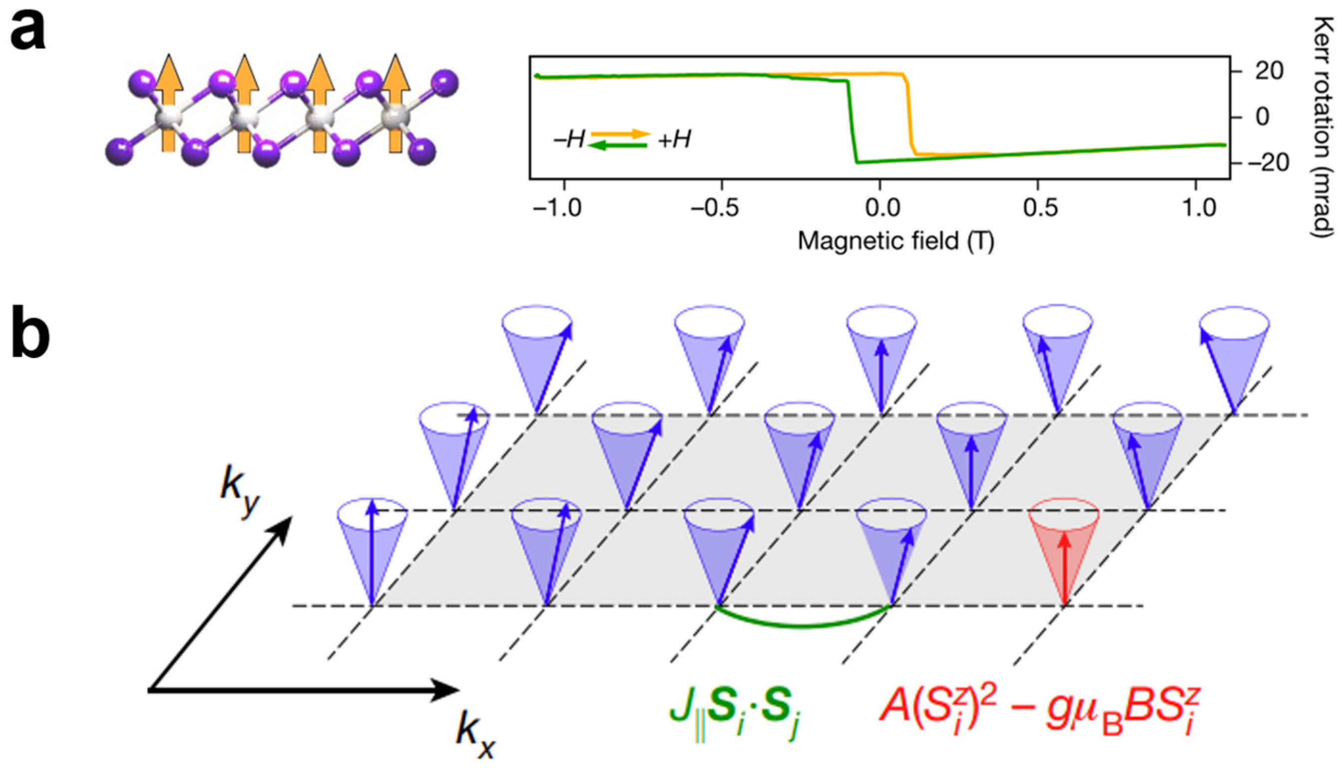
2.4. Two-Dimensional Magnetic Materials

Recent advancements in the field of 2D materials have paved the way for the exploration of novel magnetic phenomena and their applications in random access memory (MRAM) [35]. As early as 2017, 2D crystals including CrI3 and Cr2Ge2Te6 were observed to have magnetic properties (Figure 4a,b) [36,37,38]. These materials, with their well-defined layer thickness and atomically flat surfaces, allow for the manipulation of magnetic properties through electrical gating and strain engineering. Other 2D magnetic materials have also been gradually identified, such as Fe3GeTe2 [39]. The challenges of scalability [38], ambient stability [37], and Curie temperature [40] remain significant hurdles for the practical applications of 2D magnetic materials. With the continuous development of growth techniques and characterization methods, such as molecular beam epitaxy and scanning single-spin magnetometry, it is expected that these challenges will be overcome [36].

2.5. Two-Dimensional Phase-Change Materials

Great interest has been drawn to 2D phase-change materials. Two stable states of these materials can represent “0” and “1”, allowing them to be the crucial part of phase-change memory (PCM). Recent research has uncovered several 2D materials with phase-change behavior, such as InSeX (Figure 5a) [41]. InSeX can also be changed between crystalline and amorphous phases under a melt-quench-recrystallization mechanism [42]. TMD materials including molybdenum diselenide (MoSe2), MoTe2, and tungsten disulfide (WS2) can undergo phase transitions (Figure 5b) [43]. Density functional theory (DFT) calculations have revealed that MoTe2 can switch between semiconducting 2H and semimetallic 1T’ phases through mechanical strain, with the transition temperature and strain magnitude dependent on the material’s composition and the presence of adsorbed atoms or molecules [44]. Vertical lamellar MoSe2 films can undergo reversible phase transitions from the conducting 1T phase to the semiconducting 2H phase, facilitated by all-solid-state reversible intercalation of Cu cations [45].

3. Two-Dimensional Non-Volatile Memory Principles

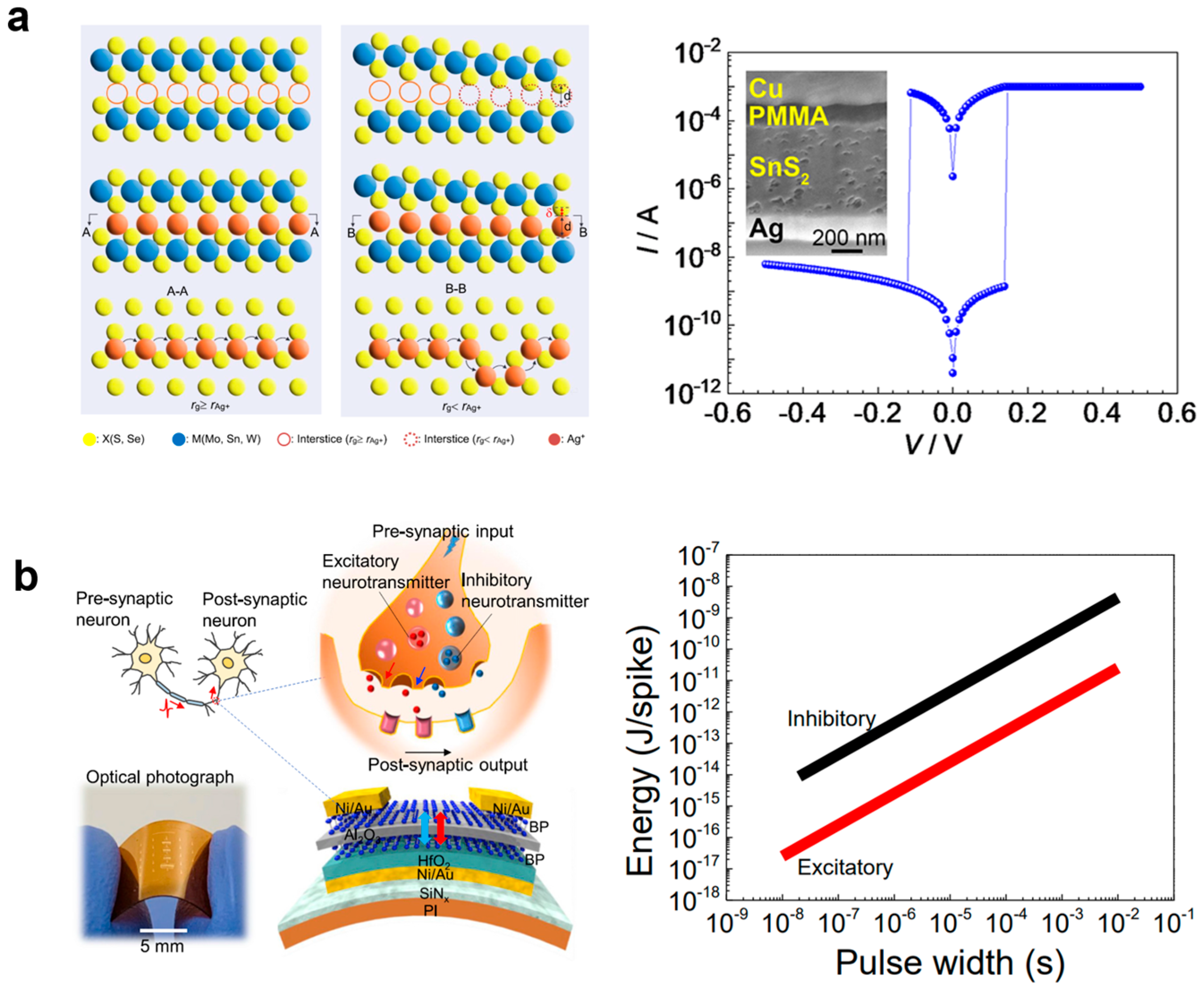
3.1. Two-Dimensional Resistive Random Access Memory

Two-dimensional resistive random access memory (RRAM) is a type of non-volatile memory with resistance switching behavior. Two-dimensional RRAM has attracted considerable interest within the field of next-generation non-volatile memory research. Many researchers focus on resistive switching behavior and try to improve the speed of 2D RRAM. Zhang et al. demonstrated an electric-field-induced structural transition in vertical MoTe2- and Mo1−xWxTe2-based RRAM devices, showcasing reproducible resistive switching within 10 ns (Figure 6a) [46]. Tang et al. emphasized the importance of 2D semiconductors in modulating switching characteristics through sulfur vacancy diffusion for the development of high-density and reliable RRAMs for memory-based computing (Figure 6b) [47].
Apart from a single RRAM device, the integration of 2D RRAM and transistors is investigated. Sivan et al. introduced a hybrid integration of 2D material-based 1T1R RRAM cells, combining WSe2 p-field-effect transistors (p-FETs) with solution-processed WSe2 RRAMs [48]. The low-temperature co-integration process yielded enhanced performance and reduced switching energy. Yang et al. integrated molybdenum disulfide transistors with metal-oxide RRAM to create 2T2R ternary content-addressable memory (TCAM) cells for parallel data search applications (Figure 6c) [49]. These cells exhibited comparable resistance ratios to commercial TCAMs while reducing the transistor count and eliminating standby power consumption.
Figure 6. Schematics of state-of-the-art 2D RRAM: (a) Vertical MoTe2- and Mo1−xWxTe2-based resistive memory. Reproduced with permission [46], Copyright 2019, Springer Nature. (b) Diagrams of the set/reset processes. Reproduced with permission [47], Copyright 2019, Springer Nature. (c) Schematics of the 2T2R and 1T1R structures based on MoS2 FETs and HfOx-based RRAMs. Reproduced with permission [49], Copyright 2022, Springer Nature.
Chips 03 00014 g006

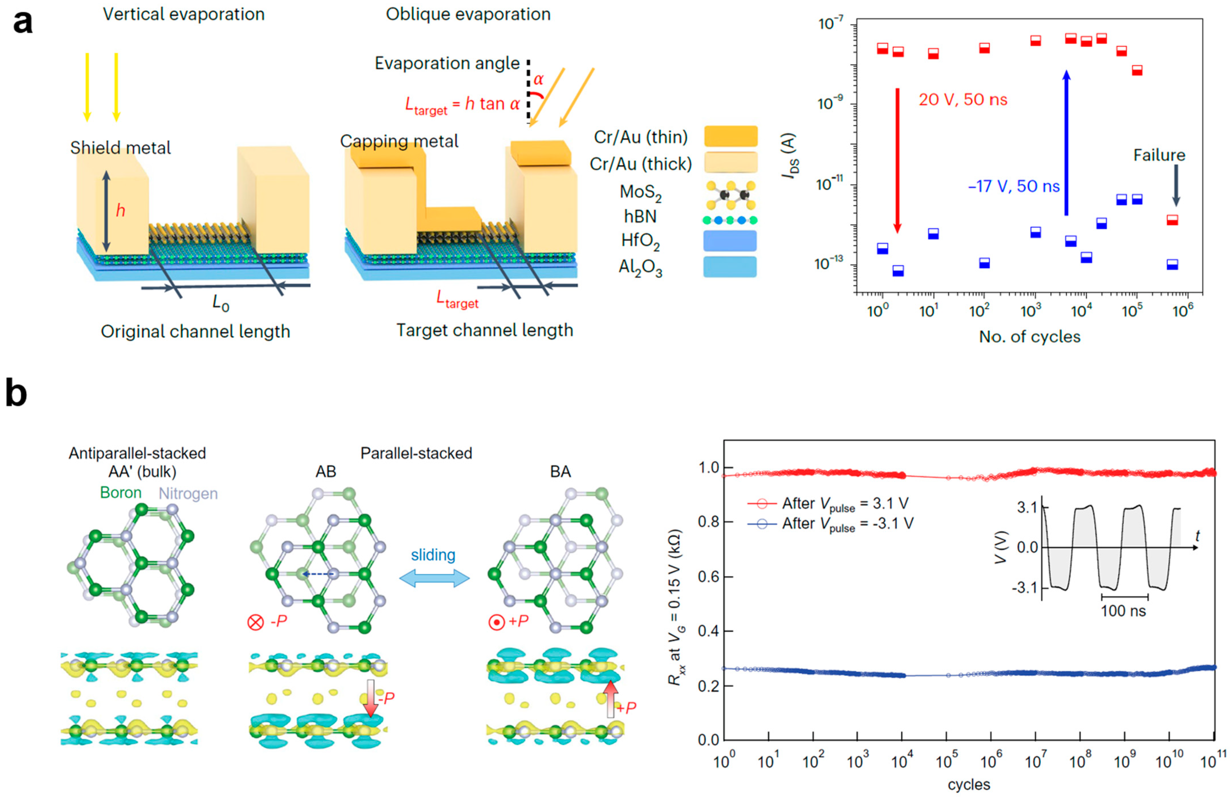
3.2. Two-Dimensional Ferroelectric Memories

The potential of ferroelectric memories for non-volatile storage and compatibility with integrated circuits has attracted the attention of researchers. Devices have been designed and illustrated through experiments in recent years. Wang et al. reported a 2D α-In2Se3 ferroelectric semiconductor channel device, and demonstrated its functions on non-volatile memory and neural computation [6]. Shen et al. put forth the concept of doping engineering in a 2D ferroelectric tunnel junction as a means of achieving a low thickness [50]. Luo et al. investigated the potential of dual-ferroelectric-coupling-engineered 2D transistors for in-memory computing, combining non-volatile logic gates and artificial synapses (Figure 7b) [51]. Jiang et al. devised an asymmetric ferroelectric-gated 2D transistor with self-rectifying photoelectric memory and artificial synapse functionality (Figure 7b) [52]. Kim et al. presented a scalable CMOS back-end-of-line-compatible AlScN/2D channel ferroelectric field-effect transistor, showcasing stable retention and endurance features suitable for integration with silicon complementary metal-oxide-semiconductor logic [53].

3.3. Two-Dimensional Magnetic Random Access Memory

Apart from RRAM and FeRAM, magnetic random access memory (MRAM) has also become a solution to the performance bottleneck. Two-dimensional magnetic vdW crystals are shown in Figure 8a [38]. The atomically thin crystalline materials exhibit magneto-optic and magnetoelectric effects. 2D magnetic crystals, including 2D ferromagnets and 2D antiferromagnets with various intra- and inter-plane magnetic configurations, can display a wide range of magneto-optic and magnetoelectric phenomena. Through spin-transfer torque (STT), spin–orbit torque (SOT), and other sorts of writing methods, the spin state of magnetic 2D materials can be shifted, which means that data stored inside 2D MRAM can be programmed (Figure 8b) [54]. Many studies are conducted to realize programming at room temperature. Wang et al. demonstrate the room-temperature magnetization switching driven by SOT in a full vdW heterostructure by an optimized epitaxial growth method [55]. Pan et al. reported all-2D magnetoresistive memory devices based on WTe2/Fe3GaTe2/BN/Fe3GaTe2 heterostructure, which can read and write data through the orbit-transfer torque (OTT) effect at room temperature [56].

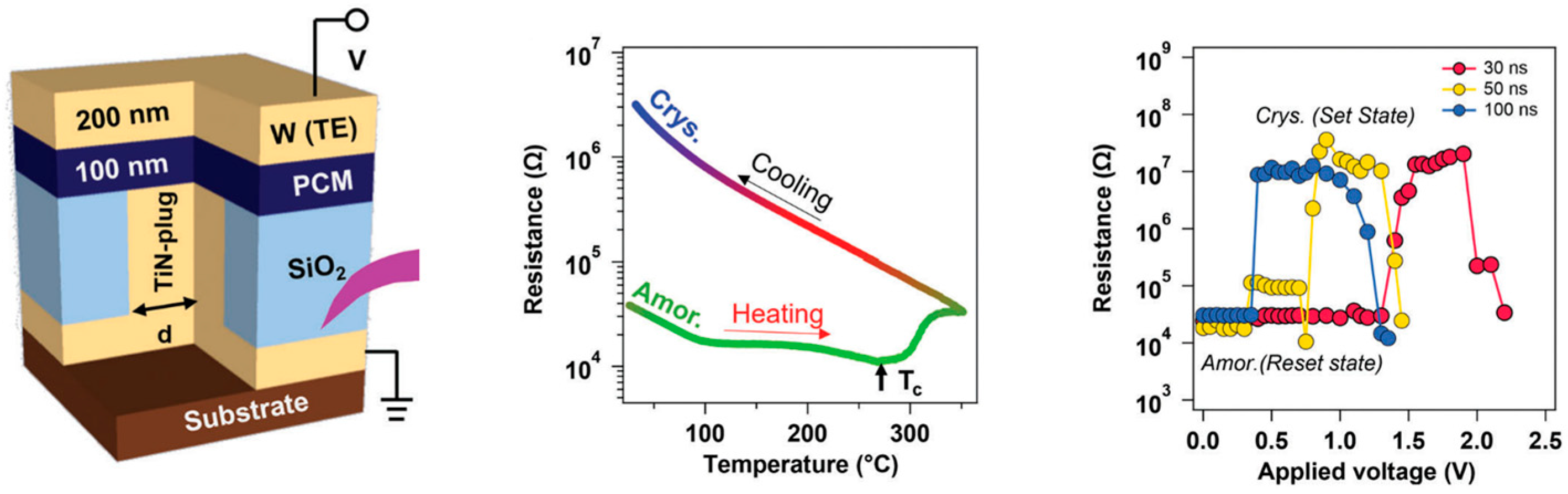
3.4. Two-Dimensional Phase-Change Memories

Both the choice of phase transition mechanism and device structure significantly impact the performance and functionality of 2D phase-change memory (PCM). The foundation of PCRAM lies in the reversible phase transitions between amorphous and crystalline states of chalcogenide materials. Two-dimensional vdW TMDs are promising to be used for PCM (Figure 9) [57]. These materials exhibit tunable electronic properties and the ability to achieve moderate phase-change temperatures. The unique properties of 2D vdW TMDs, including their ultra-low melting point and high crystallization temperature, make them attractive candidates for advanced PCRAM applications [57,58,59]. The field of phase-change memory is rapidly advancing, with innovative materials and device architectures pointing to exciting directions for the future development of highly reliable non-volatile memory solutions. These advancements open doors for new applications in data storage, neuromorphic computing, and beyond.

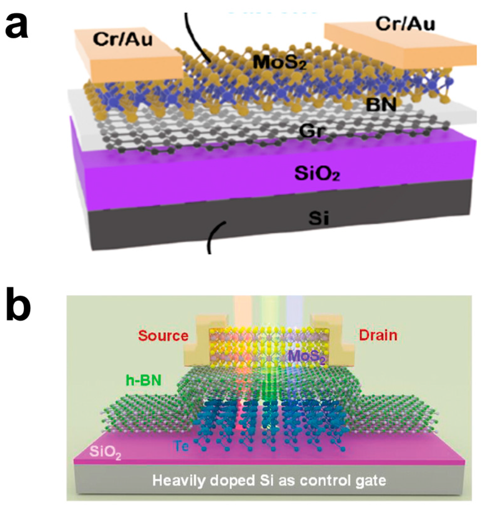
3.5. Two-Dimensional Floating Gate Memories

Floating gate memory utilizes a floating gate to store charge, enabling the retention of data even in the absence of supply. The atomic-scale thickness, absence of dangling bonds, and enhanced electrostatic control of 2D materials create interfaces free from trapped charges, enhancing the performance of floating gate memory devices [60]. The utilization of 2D materials as the channel of floating gate memories, such as TMDs like MoS2 and WSe2, offers several key advantages for floating gate memory development.
Research efforts have focused on utilizing various 2D material heterostructures to construct floating gate memory devices. Researchers have presented MoS2/BN/graphene heterostructure-based floating gate memory and demonstrated outstanding non-volatile memory characteristics [61,62,63]. The device presented by Li et al. simulates basic synaptic functions and achieves high recognition accuracy in handwritten numeral recognition tasks (Figure 10a) [63]. Li et al. explore a graphene-BP/h-BN/graphene heterostructure-based floating gate memory with ambipolar characteristics, allowing it to act as a diode and exhibit reverse rectifying behavior [64]. This heterojunction offers dual-mode non-volatile memory functionality and can be utilized in memory inverter circuits and logic rectifiers. Zha et al. demonstrate a Te-based floating gate memory with MoS2 channel that exhibits non-volatile electronic memory behaviors under intense electrical/optical stimuli with 108 extinction ratio, 100 ns switching speed, more than 4000 cycle endurance, and 4000 s retention time (Figure 10b) [65]. This demonstrates the potential of 2D floating gate memory technology for building computing systems with stable data storage.

4. Performance Criteria for Two-Dimensional Non-Volatile Memories

For the performance criteria for 2D NVMs, the specifications during the operations of each single device and performance in system-level architectures need to be considered. Power consumption evaluates the energy efficiency, and data processing speed determines the maximum working frequency. For memory switching cycles, a large switching ratio and high endurance are expected so that the device can work for many cycles. Multi-level NVMs have been developed in recent years to extend the information storage capacity compared to binary memories. Memories with high retention are needed for long-term data storage without refreshments, and low variations are required for stable values in different cycles and different devices. Most application systems of NVMs are implemented by memory arrays, so integration levels with multiple devices are considered for system-level implementations. This section discusses some of the performance criteria that have been mentioned before and analyzes the works that have achieved high performance in recent years. Summary of recently developed 2D NVMs are listed in Table 1.

4.1. Energy Consumption

Energy consumption is a crucial performance criterion for integrated circuit chips, especially for edge computing scenarios, including automatic driving vehicles, wearable electronics, and the Internet of Things, as energy supply is limited in those scenarios [73,74]. NVMs are promising for low-power devices, since the energy loss for maintaining the stored data is saved, compared to volatile memories like static random access memory (SRAM) and dynamic random access memory (DRAM) that need consistent voltage supply or data retention operations. Strategies for decreasing energy consumption have been developed recently based on the properties of two-dimensional materials.
Most energy loss of NVMs is from the write and read processes. For RRAM devices, large currents (typically larger than 10 μA) should go through the devices during write and read processes to ensure non-volatile data set behavior. Jian et al. analyzed the effect of the interstice radius between van der Waals (vdW) layers on reducing the driving force for the formation of RRAM conductive filaments, and proposed an ultra-low set power (10−10 W) and high switching ratio (106) RRAM with a 2D SnS2 layer based on the large vdW interstice radius of the SnS2-based structure (Figure 11a) [75]. Two-dimensional insulators including h-BN have superior performance for low-power RRAMs. Kang et al. developed a He+ implanted h-BN RRAM and obtained sub-pW power consumption with a 108 switching ratio by defect implanting engineering [76]. Low-power two-dimensional floating memory devices have also been developed in recent years. Tang et al. developed an all-2D van der Waals materials artificial synapse with a MoS2 channel, h-BN oxide, and graphene floating gate, and achieved energy-efficient memory switching of 18 fJ for a single pulse [71]. Xiong et al. proposed a floating gate device with a BP/Al2O3/BP structure and flexible substrate (Figure 11b) [72]. This device can be operated in ~10 ns pulses and has low energy consumption of less than 1 fJ per spike.

4.2. Data Processing Speed

Due to the state switching properties, many NVM devices have relatively larger set and reset time than volatile memories like SRAM and DRAM, which have less than 10 ns access time [77]. Since 2D material architectures are developed later than other material architectures, the data processing speed of 2D NVMs is a critical issue to be addressed for wider applications for next-generation memory devices.
Two-dimensional floating gate memories are promising for fast NVM devices. vdW heterojunctions of 2D materials have superior properties such as atomically sharp interfaces that facilitate the write and read speed of floating gate memories [78,79,80]. Wang et al. reported a semi-floating-gate-controlled lateral homojunction structure made of 2D vdW heterostructures with an ultra-fast programming time of about 20 ns for floating memory applications (Figure 12a) [81]. This design is 107 times faster than other 2D homojunctions and can be used to perform in-memory logic operations. An ultra-fast 2D floating memory with 20 ns programming time, multi-bit storage capacity, and more than 10 years of data retention based on MoS2/h-BN/MLG/h-BN/MLG vdW heterostructures was also developed later [82]. Ferroelectric memory devices can achieve fast programming speed by means of replacing normal channel materials with 2D ferroelectric semiconductors that have inherent out-of-plane and in-plane polarization directions [83]. Wang et al. developed a 2D ferroelectric α-In2Se3 memory device for NVM applications and neuromorphic computing (Figure 12b) [6]. The programming time is only 40 ns with large hysteresis windows and data retention. Two-dimensional RRAMs can achieve much higher data processing speed, due to the fast state switching of atomic thick layer of 2D insulators. Nibhanupudi et al. proposed a 120 ps switching speed memristor device based on atomically thin sheets of 2D h-BN, which can be set by ultra-short (120 ps–3 ns) voltage pulses (Figure 12c) [67]. The ultra-fast 2D memristor reaches the speed of state-of-the-art volatile memories and is promising for fast data processing scenarios.

4.3. Retention

Retention is to evaluate the duration of the device state that can persist without significant degradation or relaxation [9]. A high retention means that the memory device can store the information without refreshing for a long time. A stable value of the NVM device with negligible time decay is necessary for long-term memories and in-memory computing. Among different types of 2D NVMs, 2D ferroelectric memories have the potential to develop high-retention NVM devices. Xiang et al. fabricated a ferroelectric transistor based on a MoS2 channel and ferroelectric HfO2 (Hf0.5Zr0.5O2, HZO) oxide for neuromorphic computing (Figure 13a) [84]. An ultralong retention of at least 10 years was achieved. Ning et al. developed a duplex two-dimensional material structure with HfO2 and HZO oxide layers and a monolayer MoS2 channel to construct an in situ learning in-memory computing architecture, and more than 10 years of retention was achieved [68].
Other than developing long-retention memory devices, memory devices with short retention have also been investigated and applied to various scenarios. Sun et al. fabricated SnS-based two-dimensional memristors for language recognition [85]. Due to charge trapping and photogating effects, short-term conduction state retention is achieved by both electrical and optical stimuli. Chen et al. developed optoelectronic graded neurons based on MoS2 charge-trapping transistors (Figure 13b) [86]. The charge trapping at the interface between the MoS2 channel and oxide enables the device to have short-term retention, and an in-sensor motion perception system is constructed.

4.4. Endurance

Endurance means the ability of an NVM device to undergo a certain number of cycles while the state of the device remains stable. Endurance is quantified by the maximum number of writing cycles. In real applications, memory devices are required to keep stable after several rounds of data updates. In edge computing scenarios, when in situ learning of neural networks is required, the weights of neural networks are updated many times during the iterations of learning processes, and memory cells should be stable during the weight update.
Floating gate devices are commonly used for high-endurance devices. Two-dimensional floating gate devices are developed and exhibit large endurance. Jiang et al. proposed a scalable integration process for ultrafast 2D floating gate memory devices based on MoS2 channels with HfO2/Pt/HfO2 and Al2O3/Pt/Al2O3 memory stack (Figure 14a) [70]. A large endurance of more than 105 is exhibited in this structure. Other than 2D floating gate memories, 2D ferroelectric memories have been investigated in recent years to enhance endurance by developing high-performance 2D materials and advanced nanostructures. Sliding ferroelectricity is reported to have extremely large endurance, and sliding ferroelectric devices have been investigated recently [87]. Yasuda et al. reported a high-endurance sliding ferroelectric memory device with monolayer graphene and parallel-stacked bilayer BN (Figure 14b) [69]. This device exhibits ultrafast switching speeds on the nanosecond scale and high endurance exceeding 1011 switching cycles.

4.5. Variations

Cycle-to-cycle variation is a significant criterion to evaluate the value variations of a memory device in different data writing cycles. Low cycle-to-cycle variation is required for the high accuracy of weight update in NVM-based artificial neural networks (ANNs) with variable weights. Device-to-device variation is a critical specification for NVM arrays with multiple devices. Different devices in an NVM array need to have low enough value variations.
Low cycle-to-cycle and device-to-device variations of 2D NVMs can be achieved by high-quality growth of 2D materials and fabrication processes that have little effect on the material performance. Memory device structures with small feature sizes and high densities have the potential to be fabricated as NVM arrays with low variations; 1R RRAM arrays have the theoretical minimum feature size, i.e., 4F2 (F is the footprint), which results in their high density. Chen et al. developed high-density memristive crossbar arrays for artificial neural networks. The resistive switching medium is a chemical-vapour-deposited (CVD) multilayer h-BN with small sizes of 150 nm × 150 nm for each memristor cell (Figure 15a) [66]. The h-BN layer has high conformity, and ultralow variations of the device are achieved, i.e., 1.53% cycle-to-cycle variation and 5.74% device-to-device variation.
Figure 13. NVMs considering the retention performance: (a) A long-term retention ferroelectric transistor for neuromorphic computing. Reproduced with permission [84], Copyright 2023, Wiley-VCH. (b) A short-term retention 2D charge-trapping transistor for motion perception [86], Copyright 2023, Springer Nature.
Chips 03 00014 g013
Figure 14. High-endurance NVMs: (a) A 2D floating gate memory device with MoS2 channel exhibiting more than 105 cycle endurance. Reproduced with permission [70], Copyright 2024, Springer Nature. (b) A high-endurance 2D sliding ferroelectric memory device with high endurance exceeding 1011 switching cycles. Reproduced with permission [69], Copyright 2024, American Association for the Advancement of Science.
Chips 03 00014 g014
Apart from ANNs that require low enough cycle-to-cycle and device-to-device variations, some of the other computing architectures utilize the variations of devices and data writing cycles, and are more tolerant of variations. For example, due to the cycle-to-cycle variation, the intrinsic probability distribution of the stored values of a non-volatile memory device after data writing that approximates Gaussian distribution can be used to construct Bayesian neural networks (BNNs) [88]. Zheng et al. proposed a two-dimensional memtransistor-based BNN (Figure 15b) [89]. The BN architecture is composed of 29 devices and has a low energy cost of about 1.2 nJ. Device-to-device variations can be used in reservoir computing (RC) systems. The device-to-device variation can expand the reservoir size and improve the system’s performance [90]. The defects in 2D material interfaces can be utilized to generate device-to-device variation, and 2D RC systems have been developed in recent years to perform recurrent artificial intelligent computing with reduced hardware costs [85].
Figure 15. NVMs considering the variation performance: (a) A low-variation NVM based on high-density h-BN array. Reproduced with permission [66], Copyright 2020, Springer Nature. (b) A hardware-implemented 2D Bayesian neural network that utilizes the large variations of the device. Reproduced with permission [89], Copyright 2022, Springer Nature.
Chips 03 00014 g015

4.6. Integration

NVM devices should be integrated as multiple device-based functional systems and large-scale memory arrays to have the potential as memory devices in real cases. The polarization reconfigurable property of ferroelectric materials can be used to program the junction distribution of 2D material transistors and construct reconfigurable device systems and in-memory logic computing architectures. Tong et al. reported a WSe2-on-lithium niobate (LNO) cascaded architecture and showed the reconfigurable functions of the architecture for nonlinear transistor and NVM cells (Figure 16a) [91]. An operational amplifier based on multiple devices is also fabricated and verified. This work envisions the perspective of ferroelectric proximity effect-based 2D FeFETs on promoting module integration. Ferroelectrics can also be used for weight programming for in-sensor computing systems. Wu et al. reported ferroelectric-defined reconfigurable homojunctions and fabricated an array for in-memory sensing and computing applications [92].
Designs of NVM devices need to be compatible with the present integrated circuit technology. A promising strategy of 2D NVM integration is hybrid 2D-CMOS architecture, where circuits and units by CMOS devices are fabricated front-end-of-line, and fabrication processes for 2D NVM devices that are relatively newly developed and sensitive to process fluctuation are conducted on the top of CMOS device arrays. This back-end-of-line integration of 2D NVMs exhibits high performance. Zhu et al. reported a hybrid 2D–CMOS chip with 2D h-BN memristor and CMOS circuits for spiking neural networks (SNNs) (Figure 16b) [93]. Integrated hybrid 2D–CMOS systems are fabricated on a 200 mm wafer with memristor cells as small as 0.053 μm2. Two-dimensional NVMs can also be compatible with advanced 3D integration technology to enable large integration levels [94]. Kang et al. developed a monolithic 3D integration of 2D material memristor arrays (Figure 16c) [11]. The WSe2/h-BN memristors and MoS2 transistors are all made of 2D materials. The 3D integrated array based on 2D materials reveals an innovative design of next-generation high-density memory chips. Also, Park et al. reported lateral gated ferroelectric transistor arrays based on 2D α-In2Se3 and demonstrated 3D integration of ferroelectric arrays [95].
Figure 16. Integration of NVMs: (a) WSe2-on-LNO multifunctional architecture and a multiple device-based operational amplifier for module integration. Reproduced with permission [91], Copyright 2021, American Association for the Advancement of Science. (b) Hybrid 2D-CMOS integrated memristor chip. Reproduced with permission [93], Copyright 2023, Springer Nature. (c) Three-dimensional integration of 2D material-based memristor array. Reproduced with permission [11], Copyright 2023, Springer Nature.
Chips 03 00014 g016

5. Two-Dimensional Non-Volatile Memory Arrays for In-Memory Computing

5.1. In-Memory Computing Architecture Mechanisms

Recent years have witnessed rapid advances in artificial intelligence and edge computing. However, the growing demands of high-performance memory devices are harder to be reached by conventional von Neumann architecture applied to most computational electronics due to the large power consumption and latency caused by information transmission processes between memory units and data processing units [96,97]. To address this problem, in-memory computing architectures are proposed and developed. For in-memory computing architectures, certain tasks of data processing are performed in the memory array, avoiding a large amount of data transmission (Figure 17a) [98]. In-memory computing architectures have the perspective to exceed the present performance limit of computational electronics [99]. Recently, most research focuses on applications of matrix-vector multiplication (MVM) based on in-memory computing architectures, as MVM is the fundamental operation of common algorithms of artificial intelligence, including perceptron and neural networks [100]. Figure 17b shows a typical architecture for in-memory computing based on RRAM, where NVM cells are aligned as an array and connected as a crossbar. Each cell stores a value of weight data (w) by its conductance (g). Input signals (x) in voltage form (V) are from bit lines (BLs), and output signals in current form (I) are detected at search lines (SLs). Word lines (WLs) controlling transistors in each cell are for data writing and weight updates. During the operation of MVM, SLs are grounded and WLs are constantly high, and the output current at the ith SL according to Ohm’s law is given by
I ( i ) = j g ( i , j ) V ( j )
where i and j are serial numbers of SLs and BLs, respectively. The computation process of the array is equivalent to the MVM computation. Since devices like memristors do not have negative conductance to represent negative weight values, a commonly applied method is to double the number of cells and lines in the array, where positive cells represent positive weight values for MVM computing, and negative cells represent negative weight values. NVMs also need peripheral circuits to drive the inputs and convert output signals from the analog current form to the digital form.

5.2. In-Memory Computing Systems

In-memory computing systems are designed to mimic the operation of human brains, where computing processes are performed in memory units [10,102,103]. Most in-memory computing systems are constructed in crossbar arrays. In-memory computing artificial intelligent systems can be used to various applications [47,96,104,105], including object recognition, robot control, financial trading, etc. Liu et al. proposed a dual-gate-controlled 2D MoS2 FET with stacked HfZrOx gates for ferroelectric programming [106]. An ANN is constructed by the device for the recognition of Iris. Khan et al. proposed a floating gate memory device based on 2D material channels and demonstrated a neural network for digit classifications with about 92% accuracy (Figure 18a) [53]. Most neural network systems by NVM devices focus on forward propagation operations. The training and weight update processes of neural networks are conducted off-line. With the increasing demand for high-performance edge computing devices, there is a trend to develop in-memory computing systems that are trained in situ [100,107]. Ning et al. reported an in situ training ferroelectric memory device system based on MoS2 channel and a duplex structure for both training and inference operations (Figure 18b) [68]. The in situ training reaches 99.86% accuracy, and the work paves the way for NVM-based edge computing electronics for life-long learning applications. Apart from conventional crossbar architectures, array structures that are more efficient for artificial intelligence computations have been investigated. Liu et al. proposed a recirculated logic operation structure based on 2D MoS2 transistors and Ag/HfO2/Pt filament memristors for cellular automata (CA) evolution operations (Figure 18c) [13]. The promoted structure design significantly reduces the hardware complexity for CA operations and is reported to have a 79-fold reduction in hardware costs compared to FPGA-based counterparts. An RC system is demonstrated that reaches over 96% accuracy.

5.3. In-Memory Sensing and Computing Systems

The entire signal chain of edge computing vision architectures includes image data sensing, data storage, and computing. In conventional architecture, those functions are separated, and the extremely high cost of a large amount of data transmission restricts the performance of edge computing vision architectures [108]. Therefore, apart from in-memory computing architectures, in-sensor computing architectures for image data processing have been developed to accelerate operations of image sensing and processing [109,110]. Recently, vision systems combining in-memory sensing and computing have been developed, realizing the integration of the entire signal chain. Zhang et al. proposed a retinomorphic device based on 2D heterostructures and floating gate structures. The non-volatile hole and electron storage capability of the WSe2 floating gate enables the programming of the BP channel junction and thereby controls the direction of the photocurrent response by optical signals (Figure 19a) [111]. An integrated system for optical perception, memory, and computation is constructed. Wu et al. reported an integrated in-memory sensing and computing system based on ferroelectric-defined reconfigurable homojunctions (Figure 19b) [92]. The polarity direction of the WSe2 channel junction is defined by the ferroelectric gate, and the number of weight states is over 51 (>5 bit). Touch is another important type of sense apart from vision. Tactile in-memory sensing and computing has been investigated in recent years [112,113]. Mo et al. developed a multi-terminal MoS2 transistor with a Au nanoparticle floating gate and constructed an integrated neuromorphic system for tactile sensing and synaptic plasticity computing [114].
Figure 18. NVM device arrays for in-memory computing systems: (a) 2D floating gate memory device for artificial neural networks. Reproduced with permission [53], Copyright 2023, Elsevier Ltd. (b) Ferroelectric in-memory computing system with in situ learning. Reproduced with permission [68], Copyright 2023, Springer Nature. (c) Recirculated memristor array structure for efficient cellular automata evolution operations. Reproduced with permission [13], Copyright 2023, Springer Nature.
Chips 03 00014 g018
Figure 19. In-memory computing and sensing systems based on 2D NVMs: (a) 2D heterostructures and floating gate structure-based retinomorphic device for integrated optical perception, memory, and computation. Reproduced with permission [111], Copyright 2022, Springer Nature. (b) Ferroelectric-defined reconfigurable 2D homojunctions for integration of in-memory sensing and computing. Reproduced with permission [92], Copyright 2023, Springer Nature.
Chips 03 00014 g019

6. Conclusions and Outlooks

NVM devices are promising for constructing advanced memory systems. Two-dimensional material-based NVMs have improved performance and extended functionalities, and are candidates for next-generation memory electronics. Two-dimensional NVMs have been developed for functional integration, including in-memory computing and in-sensor computing systems, and the combination systems of the entire signal chain. This review discussed 2D materials with different properties, NVM devices based on 2D materials, performance criteria of 2D NVMs, and the integration of 2D NVM arrays for in-memory computing systems. In the future, novel 2D materials with more advanced performance and new properties have the potential to be explored; NVM devices should be improved by novel 2D materials with more advanced performance, alongside innovative structures for lower power consumption, larger data retention, faster data setting and resetting, and higher integration levels. Moreover, novel operation mechanisms should be researched by improving the designs of NVM cell structures, reconstructing array circuit diagrams, and developing efficient computational system architectures for specific scenarios to exceed the present performance limit of processor systems. The functional integration of signal processing including in-memory computing and sensing needs to be further improved for higher device consistency and larger integration for practical cases. Besides vision processing systems, multisensory processing including tactile, olfactory, and acoustic in-memory sensing and computing systems needs to be developed in the future. To achieve commercialization and applications of 2D NVMs in the future, stable and large-scale production of high-performance 2D materials by large-area growth such as CVD and epitaxial growth should be developed. Fabrication processes of 2D NVMs with sufficiently high yield and integration levels should be constructed. Algorithms and system-level designs of novel computing architectures including compute-in-memory architectures and SNNs that can fit with 2D NVM systems should also be further progressed to reach sufficiently high performance to be used in real cases.

Author Contributions

Writing—original draft preparation, J.P. and Z.W.; writing—review and editing, J.P., Z.W., B.Z., J.Y. and P.G.; supervision, T.-L.R. and Y.Y.; funding acquisition, T.-L.R. and Y.Y. All authors have read and agreed to the published version of the manuscript.

Funding

This research was supported by the National Key R&D Program (2022YFB3204100, 2021YFC3002200), the National Natural Science Foundation of China (U20A20168), the Research Fund from Tsinghua University Initiative Scientific Research Program, and a grant from the Guoqiang Institute, Tsinghua University.

Institutional Review Board Statement

Not applicable.

Informed Consent Statement

Not applicable.

Data Availability Statement

No new data were created or analyzed in this study. Data sharing is not applicable to this article.

Conflicts of Interest

The authors declare no conflict of interest.

References

  1. Liu, A.; Zhang, X.; Liu, Z.; Li, Y.; Peng, X.; Li, X.; Qin, Y.; Hu, C.; Qiu, Y.; Jiang, H.; et al. The Roadmap of 2D Materials and Devices Toward Chips. Nanomicro Lett. 2024, 16, 119. [Google Scholar] [CrossRef] [PubMed]
  2. Wu, F.; Tian, H.; Shen, Y.; Hou, Z.; Ren, J.; Gou, G.; Sun, Y.; Yang, Y.; Ren, T.L. Vertical MoS2 transistors with sub-1-nm gate lengths. Nature 2022, 603, 259–264. [Google Scholar] [CrossRef] [PubMed]
  3. Shen, Y.; Dong, Z.; Sun, Y.; Guo, H.; Wu, F.; Li, X.; Tang, J.; Liu, J.; Wu, X.; Tian, H.; et al. The Trend of 2D Transistors toward Integrated Circuits: Scaling Down and New Mechanisms. Adv. Mater. 2022, 34, e2201916. [Google Scholar] [CrossRef] [PubMed]
  4. Jiang, J.; Xu, L.; Qiu, C.; Peng, L.M. Ballistic two-dimensional InSe transistors. Nature 2023, 616, 470–475. [Google Scholar] [CrossRef] [PubMed]
  5. Dong, L.; Jia, R.; Xin, B.; Peng, B.; Zhang, Y. Effects of oxygen vacancies on the structural and optical properties of β-Ga2O3. Sci. Rep. 2017, 7, 40160. [Google Scholar] [CrossRef]
  6. Wang, S.; Liu, L.; Gan, L.; Chen, H.; Hou, X.; Ding, Y.; Ma, S.; Zhang, D.W.; Zhou, P. Two-dimensional ferroelectric channel transistors integrating ultra-fast memory and neural computing. Nat. Commun. 2021, 12, 53. [Google Scholar] [CrossRef]
  7. Mi, M.; Xiao, H.; Yu, L.; Zhang, Y.; Wang, Y.; Cao, Q.; Wang, Y. Two-dimensional magnetic materials for spintronic devices. Mater. Today Nano 2023, 24, 100408. [Google Scholar] [CrossRef]
  8. Jiao, F.; Chen, B.; Ding, K.; Li, K.; Wang, L.; Zeng, X.; Rao, F. Monatomic 2D phase-change memory for precise neuromorphic computing. Appl. Mater. Today 2020, 20, 100641. [Google Scholar] [CrossRef]
  9. Zhou, H.; Li, S.; Ang, K.W.; Zhang, Y.W. Recent Advances in In-Memory Computing: Exploring Memristor and Memtransistor Arrays with 2D Materials. Nano-Micro Lett. 2024, 16, 121. [Google Scholar] [CrossRef]
  10. Zhang, Q.; Zhang, Z.; Li, C.; Xu, R.; Yang, D.; Sun, L. Van der Waals materials-based floating gate memory for neuromorphic computing. Chip 2023, 2, 100059. [Google Scholar] [CrossRef]
  11. Kang, J.H.; Shin, H.; Kim, K.S.; Song, M.K.; Lee, D.; Meng, Y.; Choi, C.; Suh, J.M.; Kim, B.J.; Kim, H.; et al. Monolithic 3D integration of 2D materials-based electronics towards ultimate edge computing solutions. Nat. Mater. 2023, 22, 1470–1477. [Google Scholar] [CrossRef] [PubMed]
  12. Radisavljevic, B.; Radenovic, A.; Brivio, J.; Giacometti, V.; Kis, A. Single-layer MoS2 transistors. Nat. Nanotechnol. 2011, 6, 147–150. [Google Scholar] [CrossRef] [PubMed]
  13. Liu, Y.; Tian, H.; Wu, F.; Liu, A.; Li, Y.; Sun, H.; Lanza, M.; Ren, T.L. Cellular automata imbedded memristor-based recirculated logic in-memory computing. Nat. Commun. 2023, 14, 2695. [Google Scholar] [CrossRef] [PubMed]
  14. Li, X.; Zhou, P.; Hu, X.; Rivers, E.; Watanabe, K.; Taniguchi, T.; Akinwande, D.; Friedman, J.S.; Incorvia, J.A.C. Cascaded Logic Gates Based on High-Performance Ambipolar Dual-Gate WSe2 Thin Film Transistors. ACS Nano 2023, 17, 12798–12808. [Google Scholar] [CrossRef]
  15. Chen, J.; Li, P.; Zhu, J.; Wu, X.-M.; Liu, R.; Wan, J.; Ren, T.-L. Reconfigurable MoTe2 Field-Effect Transistors and its Application in Compact CMOS Circuits. IEEE Trans. Electron Devices 2021, 68, 4748–4753. [Google Scholar] [CrossRef]
  16. Ahmed, Z.; Afzalian, A.; Schram, T.; Jang, D.; Verreck, D.; Smets, Q.; Schuddinck, P.; Chehab, B.; Sutar, S.; Arutchelvan, G.; et al. Introducing 2D-FETs in Device Scaling Roadmap using DTCO. In Proceedings of the 2020 IEEE International Electron Devices Meeting (IEDM), San Francisco, CA, USA, 12–18 December 2020; pp. 22.25.21–22.25.24. [Google Scholar]
  17. Chen, H.; Xue, X.; Liu, C.; Fang, J.; Wang, Z.; Wang, J.; Zhang, D.W.; Hu, W.; Zhou, P. Logic gates based on neuristors made from two-dimensional materials. Nat. Electron. 2021, 4, 399–404. [Google Scholar] [CrossRef]
  18. Pan, C.; Wang, C.-Y.; Liang, S.-J.; Wang, Y.; Cao, T.; Wang, P.; Wang, C.; Wang, S.; Cheng, B.; Gao, A.; et al. Reconfigurable logic and neuromorphic circuits based on electrically tunable two-dimensional homojunctions. Nat. Electron. 2020, 3, 383–390. [Google Scholar] [CrossRef]
  19. Shen, P.C.; Su, C.; Lin, Y.; Chou, A.S.; Cheng, C.C.; Park, J.H.; Chiu, M.H.; Lu, A.Y.; Tang, H.L.; Tavakoli, M.M.; et al. Ultralow contact resistance between semimetal and monolayer semiconductors. Nature 2021, 593, 211–217. [Google Scholar] [CrossRef]
  20. Jiang, J.; Xu, L.; Du, L.; Li, L.; Zhang, G.; Qiu, C.; Peng, L.-M. Yttrium-doping-induced metallization of molybdenum disulfide for ohmic contacts in two-dimensional transistors. Nat. Electron. 2024, 7, 545–556. [Google Scholar] [CrossRef]
  21. Zhang, Q.; Wang, X.-F.; Shen, S.-H.; Lu, Q.; Liu, X.; Li, H.; Zheng, J.; Yu, C.-P.; Zhong, X.; Gu, L.; et al. Simultaneous synthesis and integration of two-dimensional electronic components. Nat. Electron. 2019, 2, 164–170. [Google Scholar] [CrossRef]
  22. Yang, S.; Lee, G.; Kim, J. Selective p-Doping of 2D WSe2 via UV/Ozone Treatments and Its Application in Field-Effect Transistors. ACS Appl. Mater. Interfaces 2021, 13, 955–961. [Google Scholar] [CrossRef] [PubMed]
  23. Cao, W.; Kang, J.; Sarkar, D.; Liu, W.; Banerjee, K. 2D Semiconductor FETs—Projections and Design for Sub-10 nm VLSI. IEEE Trans. Electron Devices 2015, 62, 3459–3469. [Google Scholar] [CrossRef]
  24. Knobloch, T.; Illarionov, Y.Y.; Ducry, F.; Schleich, C.; Wachter, S.; Watanabe, K.; Taniguchi, T.; Mueller, T.; Waltl, M.; Lanza, M.; et al. The performance limits of hexagonal boron nitride as an insulator for scaled CMOS devices based on two-dimensional materials. Nat. Electron. 2021, 4, 98–108. [Google Scholar] [CrossRef]
  25. Afshari, S.; Xie, J.; Musisi-Nkambwe, M.; Radhakrishnan, S.; Sanchez Esqueda, I. Unsupervised learning in hexagonal boron nitride memristor-based spiking neural networks. Nanotechnology 2023, 34, 445703. [Google Scholar] [CrossRef] [PubMed]
  26. Yuan, B.; Liang, X.; Zhong, L.; Shi, Y.; Palumbo, F.; Chen, S.; Hui, F.; Jing, X.; Villena, M.A.; Jiang, L.; et al. 150 nm × 200 nm Cross-Point Hexagonal Boron Nitride-Based Memristors. Adv. Electron. Mater. 2020, 6, 1900115. [Google Scholar] [CrossRef]
  27. Afshari, S.; Radhakrishnan, S.; Xie, J.; Musisi-Nkambwe, M.; Meng, J.; He, W.X.; Seo, J.S.; Esqueda, I.S. Dot-product computation and logistic regression with 2D hexagonal-boron nitride (h-BN) memristor arrays. 2D Materials 2023, 10, 035031. [Google Scholar] [CrossRef]
  28. Zhao, Y.; Lou, Z.; Hu, J.; Li, Z.; Xu, L.; Chen, Z.; Xu, Z.; Wang, T.; Wu, M.; Ying, H.; et al. Scalable Layer-Controlled Oxidation of Bi2O2Se for Self-Rectifying Memristor Arrays with sub-pA Sneak Currents. Adv. Mater. 2024. Early View. [Google Scholar] [CrossRef]
  29. Io, W.F.; Pang, S.; Wong, L.W.; Zhao, Y.; Ding, R.; Mao, J.; Zhao, Y.; Guo, F.; Yuan, S.; Zhao, J.; et al. Direct observation of intrinsic room-temperature ferroelectricity in 2D layered CuCrP2S6. Nat. Commun. 2023, 14, 7304. [Google Scholar] [CrossRef]
  30. Liu, C.; Guan, S.; Yin, H.; Wan, W.; Wang, Y.; Zhang, Y. γ-GeSe: A two-dimensional ferroelectric material with doping-induced ferromagnetism. Appl. Phys. Lett. 2019, 115, 252904. [Google Scholar] [CrossRef]
  31. Zhu, L.; Lu, Y.; Wang, L. Tuning ferroelectricity by charge doping in two-dimensional SnSe. J. Appl. Phys. 2020, 127, 014101. [Google Scholar] [CrossRef]
  32. Hou, P.; Lv, Y.; Chen, Y.; Liu, Y.; Wang, C.; Zhou, P.; Zhong, X.; Wang, J.; Ouyang, X. In-Plane Strain-Modulated Photoresponsivity of the α-In2Se3-Based Flexible Transistor. ACS Appl. Electron. Mater. 2019, 2, 140–146. [Google Scholar] [CrossRef]
  33. Li, B.; Li, S.; Wang, H.; Chen, L.; Liu, L.; Feng, X.; Li, Y.; Chen, J.; Gong, X.; Ang, K.W. An Electronic Synapse Based on 2D Ferroelectric CuInP2S6. Adv. Electron. Mater. 2020, 6, 2000760. [Google Scholar] [CrossRef]
  34. Li, Y.; Fu, J.; Mao, X.; Chen, C.; Liu, H.; Gong, M.; Zeng, H. Enhanced bulk photovoltaic effect in two-dimensional ferroelectric CuInP2S6. Nat. Commun. 2021, 12, 5896. [Google Scholar] [CrossRef] [PubMed]
  35. Burch, K.S.; Mandrus, D.; Park, J.G. Magnetism in two-dimensional van der Waals materials. Nature 2018, 563, 47–52. [Google Scholar] [CrossRef]
  36. Huang, B.; Clark, G.; Navarro-Moratalla, E.; Klein, D.R.; Cheng, R.; Seyler, K.L.; Zhong, D.; Schmidgall, E.; McGuire, M.A.; Cobden, D.H.; et al. Layer-dependent ferromagnetism in a van der Waals crystal down to the monolayer limit. Nature 2017, 546, 270–273. [Google Scholar] [CrossRef]
  37. Gong, C.; Li, L.; Li, Z.; Ji, H.; Stern, A.; Xia, Y.; Cao, T.; Bao, W.; Wang, C.; Wang, Y.; et al. Discovery of intrinsic ferromagnetism in two-dimensional van der Waals crystals. Nature 2017, 546, 265–269. [Google Scholar] [CrossRef]
  38. Gong, C.; Zhang, X. Two-dimensional magnetic crystals and emergent heterostructure devices. Science 2019, 363, eaav4450. [Google Scholar] [CrossRef]
  39. Deng, Y.; Yu, Y.; Song, Y.; Zhang, J.; Wang, N.Z.; Sun, Z.; Yi, Y.; Wu, Y.Z.; Wu, S.; Zhu, J.; et al. Gate-tunable room-temperature ferromagnetism in two-dimensional Fe3GeTe2. Nature 2018, 563, 94–99. [Google Scholar] [CrossRef]
  40. Bonilla, M.; Kolekar, S.; Ma, Y.; Diaz, H.C.; Kalappattil, V.; Das, R.; Eggers, T.; Gutierrez, H.R.; Phan, M.H.; Batzill, M. Strong room-temperature ferromagnetism in VSe2 monolayers on van der Waals substrates. Nat. Nanotechnol. 2018, 13, 289–293. [Google Scholar] [CrossRef]
  41. Hu, C.; Zhu, Z.; Li, W. Two-dimensional phase-change chalcohalides. Mater. Today Nano 2023, 24, 100433. [Google Scholar] [CrossRef]
  42. Jacobs-Gedrim, R.B.; Murphy, M.T.; Yang, F.; Jain, N.; Shanmugam, M.; Song, E.S.; Kandel, Y.; Hesamaddin, P.; Yu, H.Y.; Anantram, M.P.; et al. Reversible phase-change behavior in two-dimensional antimony telluride (Sb2Te3) nanosheets. Appl. Phys. Lett. 2018, 112, 133101. [Google Scholar] [CrossRef]
  43. Duerloo, K.-A.N.; Li, Y.; Reed, E.J. Structural phase transitions in two-dimensional Mo- and W-dichalcogenide monolayers. Nat. Commun. 2014, 5, 4214. [Google Scholar] [CrossRef]
  44. Zhou, Y.; Reed, E.J. Structural Phase Stability Control of Monolayer MoTe2 with Adsorbed Atoms and Molecules. J. Phys. Chem. C 2015, 119, 21674–21680. [Google Scholar] [CrossRef]
  45. Lee, L.; Chiang, C.-H.; Shen, Y.-C.; Wu, S.-C.; Shih, Y.-C.; Yang, T.-Y.; Hsu, Y.-C.; Cyu, R.-H.; Yu, Y.-J.; Hsieh, S.-H.; et al. Rational Design on Polymorphous Phase Switching in Molybdenum Diselenide-Based Memristor Assisted by All-Solid-State Reversible Intercalation toward Neuromorphic Application. ACS Nano 2022, 17, 84–93. [Google Scholar] [CrossRef] [PubMed]
  46. Zhang, F.; Zhang, H.; Krylyuk, S.; Milligan, C.A.; Zhu, Y.; Zemlyanov, D.Y.; Bendersky, L.A.; Burton, B.P.; Davydov, A.V.; Appenzeller, J. Electric-field induced structural transition in vertical MoTe2- and Mo1−xWxTe2-based resistive memories. Nat. Mater. 2019, 18, 55–61. [Google Scholar] [CrossRef]
  47. Tang, B.; Veluri, H.; Li, Y.; Yu, Z.G.; Waqar, M.; Leong, J.F.; Sivan, M.; Zamburg, E.; Zhang, Y.W.; Wang, J.; et al. Wafer-scale solution-processed 2D material analog resistive memory array for memory-based computing. Nat. Commun. 2022, 13, 3037. [Google Scholar] [CrossRef] [PubMed]
  48. Sivan, M.; Li, Y.; Veluri, H.; Zhao, Y.; Tang, B.; Wang, X.; Zamburg, E.; Leong, J.F.; Niu, J.X.; Chand, U.; et al. All WSe2 1T1R resistive RAM cell for future monolithic 3D embedded memory integration. Nat. Commun. 2019, 10, 5201. [Google Scholar] [CrossRef]
  49. Yang, R.; Li, H.; Smithe, K.K.H.; Kim, T.R.; Okabe, K.; Pop, E.; Fan, J.A.; Wong, H.S.P. Ternary content-addressable memory with MoS2 transistors for massively parallel data search. Nat. Electron. 2019, 2, 108–114. [Google Scholar] [CrossRef]
  50. Shen, X.-W.; Fang, Y.-W.; Tian, B.-B.; Duan, C.-G. Two-Dimensional Ferroelectric Tunnel Junction: The Case of Monolayer In:SnSe/SnSe/Sb:SnSe Homostructure. ACS Appl. Electron. Mater. 2019, 1, 1133–1140. [Google Scholar] [CrossRef]
  51. Luo, Z.D.; Zhang, S.; Liu, Y.; Zhang, D.; Gan, X.; Seidel, J.; Liu, Y.; Han, G.; Alexe, M.; Hao, Y. Dual-Ferroelectric-Coupling-Engineered Two-Dimensional Transistors for Multifunctional In-Memory Computing. ACS Nano 2022, 16, 3362–3372. [Google Scholar] [CrossRef]
  52. Jiang, Y.; Zhang, L.; Wang, R.; Li, H.; Li, L.; Zhang, S.; Li, X.; Su, J.; Song, X.; Xia, C. Asymmetric Ferroelectric-Gated Two-Dimensional Transistor Integrating Self-Rectifying Photoelectric Memory and Artificial Synapse. ACS Nano 2022, 16, 11218–11226. [Google Scholar] [CrossRef] [PubMed]
  53. Khan, M.A.; Yim, S.; Rehman, S.; Ghafoor, F.; Kim, H.; Patil, H.; Khan, M.F.; Eom, J. Two-dimensional materials memory devices with floating metal gate for neuromorphic applications. Mater. Today Adv. 2023, 20, 100438. [Google Scholar] [CrossRef]
  54. Yang, H.; Valenzuela, S.O.; Chshiev, M.; Couet, S.; Dieny, B.; Dlubak, B.; Fert, A.; Garello, K.; Jamet, M.; Jeong, D.E.; et al. Two-dimensional materials prospects for non-volatile spintronic memories. Nature 2022, 606, 663–673. [Google Scholar] [CrossRef]
  55. Wang, H.; Wu, H.; Zhang, J.; Liu, Y.; Chen, D.; Pandey, C.; Yin, J.; Wei, D.; Lei, N.; Shi, S.; et al. Room temperature energy-efficient spin-orbit torque switching in two-dimensional van der Waals Fe3GeTe2 induced by topological insulators. Nat. Commun. 2023, 14, 5173. [Google Scholar] [CrossRef]
  56. Pan, Z.C.; Li, D.; Ye, X.G.; Chen, Z.; Chen, Z.H.; Wang, A.Q.; Tian, M.; Yao, G.; Liu, K.; Liao, Z.M. Room-temperature orbit-transfer torque enabling van der Waals magnetoresistive memories. Sci. Bull. 2023, 68, 2743–2749. [Google Scholar] [CrossRef] [PubMed]
  57. Shuang, Y.; Chen, Q.; Kim, M.; Wang, Y.; Saito, Y.; Hatayama, S.; Fons, P.; Ando, D.; Kubo, M.; Sutou, Y. NbTe4 Phase-Change Material: Breaking the Phase-Change Temperature Balance in 2D Van der Waals Transition-Metal Binary Chalcogenide. Adv. Mater. 2023, 35, 2303646. [Google Scholar] [CrossRef]
  58. Hatayama, S.; Saito, Y.; Makino, K.; Uchida, N.; Shuang, Y.; Mori, S.; Sutou, Y.; Krbal, M.; Fons, P. Phase control of sputter-grown large-area MoTe2 films by preferential sublimation of Te: Amorphous, 1T’ and 2H phases. J. Mater. Chem. C 2022, 10, 10627–10635. [Google Scholar] [CrossRef]
  59. Krbal, M.; Prokop, V.; Kononov, A.A.; Pereira, J.R.; Mistrik, J.; Kolobov, A.V.; Fons, P.J.; Saito, Y.; Hatayama, S.; Shuang, Y.; et al. Amorphous-to-Crystal Transition in Quasi-Two-Dimensional MoS2: Implications for 2D Electronic Devices. ACS Appl. Nano Mater. 2021, 4, 8834–8844. [Google Scholar] [CrossRef]
  60. Migliato Marega, G.; Zhao, Y.; Avsar, A.; Wang, Z.; Tripathi, M.; Radenovic, A.; Kis, A. Logic-in-memory based on an atomically thin semiconductor. Nature 2020, 587, 72–77. [Google Scholar] [CrossRef]
  61. Wu, H.; Cui, Y.; Xu, J.; Yan, Z.; Xie, Z.; Hu, Y.; Zhu, S. Multifunctional Half-Floating-Gate Field-Effect Transistor Based on MoS2–BN–Graphene van der Waals Heterostructures. Nano Lett. 2022, 22, 2328–2333. [Google Scholar] [CrossRef]
  62. Sasaki, T.; Ueno, K.; Taniguchi, T.; Watanabe, K.; Nishimura, T.; Nagashio, K. Material and Device Structure Designs for 2D Memory Devices Based on the Floating Gate Voltage Trajectory. ACS Nano 2021, 15, 6658–6668. [Google Scholar] [CrossRef] [PubMed]
  63. Li, W.; Li, J.; Chen, Y.; Chen, Z.; Li, W.; Wang, Z.; Mu, T.; Chen, Z.; Yang, R.; Meng, Z.; et al. Demonstration of Nonvolatile Storage and Synaptic Functions in All-Two-Dimensional Floating-Gate Transistors Based on MoS2 Channels. ACS Appl. Electron. Mater. 2023, 5, 4354–4362. [Google Scholar] [CrossRef]
  64. Li, D.; Chen, M.; Zong, Q.; Zhang, Z. Floating-Gate Manipulated Graphene-Black Phosphorus Heterojunction for Nonvolatile Ambipolar Schottky Junction Memories, Memory Inverter Circuits, and Logic Rectifiers. Nano Lett. 2017, 17, 6353–6359. [Google Scholar] [CrossRef] [PubMed]
  65. Zha, J.; Xia, Y.; Shi, S.; Huang, H.; Li, S.; Qian, C.; Wang, H.; Yang, P.; Zhang, Z.; Meng, Y.; et al. A 2D Heterostructure-Based Multifunctional Floating Gate Memory Device for Multimodal Reservoir Computing. Adv. Mater. 2023, 36, 2308502. [Google Scholar] [CrossRef]
  66. Chen, S.; Mahmoodi, M.R.; Shi, Y.; Mahata, C.; Yuan, B.; Liang, X.; Wen, C.; Hui, F.; Akinwande, D.; Strukov, D.B.; et al. Wafer-scale integration of two-dimensional materials in high-density memristive crossbar arrays for artificial neural networks. Nat. Electron. 2020, 3, 638–645. [Google Scholar] [CrossRef]
  67. Teja Nibhanupudi, S.S.; Roy, A.; Veksler, D.; Coupin, M.; Matthews, K.C.; Disiena, M.; Ansh; Singh, J.V.; Gearba-Dolocan, I.R.; Warner, J.; et al. Ultra-fast switching memristors based on two-dimensional materials. Nat. Commun. 2024, 15, 2334. [Google Scholar] [CrossRef]
  68. Ning, H.; Yu, Z.; Zhang, Q.; Wen, H.; Gao, B.; Mao, Y.; Li, Y.; Zhou, Y.; Zhou, Y.; Chen, J.; et al. An in-memory computing architecture based on a duplex two-dimensional material structure for in situ machine learning. Nat. Nanotechnol. 2023, 18, 493–500. [Google Scholar] [CrossRef]
  69. Yasuda, K.; Zalys-Geller, E.; Wang, X.; Bennett, D.; Cheema, S.S.; Watanabe, K.; Taniguchi, T.; Kaxiras, E.; Jarillo-Herrero, P.; Ashoori, R. Ultrafast high-endurance memory based on sliding ferroelectrics. Science 2024, 385, 53–56. [Google Scholar] [CrossRef]
  70. Jiang, Y.; Liu, C.; Cao, Z.; Li, C.; Liu, Z.; Wang, C.; Xiang, Y.; Zhou, P. A scalable integration process for ultrafast two-dimensional flash memory. Nat. Electron. 2024, 1–8. [Google Scholar] [CrossRef]
  71. Tang, J.; He, C.; Tang, J.; Yue, K.; Zhang, Q.; Liu, Y.; Wang, Q.; Wang, S.; Li, N.; Shen, C.; et al. A Reliable All-2D Materials Artificial Synapse for High Energy-Efficient Neuromorphic Computing. Adv. Funct. Mater. 2021, 31, 2011083. [Google Scholar] [CrossRef]
  72. Xiong, X.; Wang, X.; Hu, Q.; Li, X.; Wu, Y. Flexible synaptic floating gate devices with dual electrical modulation based on ambipolar black phosphorus. iScience 2022, 25, 103947. [Google Scholar] [CrossRef] [PubMed]
  73. Jahannia, B.; Ghasemi, S.A.; Farbeh, H. An Energy Efficient Multi-Retention STT-MRAM Memory Architecture for IoT Applications. IEEE Trans. Circuits Syst. II Express Briefs 2024, 71, 1431–1435. [Google Scholar] [CrossRef]
  74. Gargari, M.A.; Eslami, N.; Moaiyeri, M.H. A Reconfigurable Non-Volatile Memory Architecture for Prolonged Wearable Health Monitoring Devices. IEEE Trans. Consum. Electron. 2024, 70, 4717–4728. [Google Scholar] [CrossRef]
  75. Jian, J.; Dong, P.; Jian, Z.; Zhao, T.; Miao, C.; Chang, H.; Chen, J.; Chen, Y.F.; Chen, Y.B.; Feng, H.; et al. Ultralow-Power RRAM with a High Switching Ratio Based on the Large van der Waals Interstice Radius of TMDs. ACS Nano 2022, 16, 20445–20456. [Google Scholar] [CrossRef]
  76. Kang, Y.; Ma, W.; Wen, X.; Xu, Y.; Hu, H.; Zhao, Y.; Yu, B. Defect Engineering in Multilayer h-BN Based RRAM by Localized Helium Ion Irradiation. IEEE Electron Device Lett. 2024, 45, 586–589. [Google Scholar] [CrossRef]
  77. Wang, F.; Hamdi, M. Matching the speed gap between SRAM and DRAM. In Proceedings of the 2008 International Conference on High Performance Switching and Routing, Shanghai, China, 15–17 May 2008; pp. 104–109. [Google Scholar]
  78. Wu, L.; Wang, A.; Shi, J.; Yan, J.; Zhou, Z.; Bian, C.; Ma, J.; Ma, R.; Liu, H.; Chen, J.; et al. Atomically sharp interface enabled ultrahigh-speed non-volatile memory devices. Nat. Nanotechnol. 2021, 16, 882–887. [Google Scholar] [CrossRef]
  79. Liu, L.; Liu, C.; Jiang, L.; Li, J.; Ding, Y.; Wang, S.; Jiang, Y.G.; Sun, Y.B.; Wang, J.; Chen, S.; et al. Ultrafast non-volatile flash memory based on van der Waals heterostructures. Nat. Nanotechnol. 2021, 16, 874–881. [Google Scholar] [CrossRef]
  80. Li, Y.; Zhang, Z.C.; Li, J.; Chen, X.D.; Kong, Y.; Wang, F.D.; Zhang, G.X.; Lu, T.B.; Zhang, J. Low-voltage ultrafast nonvolatile memory via direct charge injection through a threshold resistive-switching layer. Nat. Commun. 2022, 13, 4591. [Google Scholar] [CrossRef]
  81. Wang, H.; Bao, L.; Guzman, R.; Wu, K.; Wang, A.; Liu, L.; Wu, L.; Chen, J.; Huan, Q.; Zhou, W.; et al. Ultrafast-Programmable 2D Homojunctions Based on van der Waals Heterostructures on a Silicon Substrate. Adv. Mater. 2023, 35, 2301067. [Google Scholar] [CrossRef]
  82. Wang, H.; Guo, H.; Guzman, R.; JiaziLa, N.; Wu, K.; Wang, A.; Liu, X.; Liu, L.; Wu, L.; Chen, J.; et al. Ultrafast Non-Volatile Floating-Gate Memory Based on All-2D Materials. Adv. Mater. 2024, 36, e2311652. [Google Scholar] [CrossRef]
  83. Joo, Y.; Hwang, E.; Hong, H.; Cho, S.; Yang, H. Memory and Synaptic Devices Based on Emerging 2D Ferroelectricity. Adv. Electron. Mater. 2023, 9, 2300211. [Google Scholar] [CrossRef]
  84. Xiang, H.; Chien, Y.C.; Li, L.; Zheng, H.; Li, S.; Duong, N.T.; Shi, Y.; Ang, K.W. Enhancing Memory Window Efficiency of Ferroelectric Transistor for Neuromorphic Computing via Two-Dimensional Materials Integration. Adv. Funct. Mater. 2023, 33, 2304657. [Google Scholar] [CrossRef]
  85. Sun, L.; Wang, Z.; Jiang, J.; Kim, Y.; Joo, B.; Zheng, S.; Lee, S.; Yu, W.J.; Kong, B.S.; Yang, H. In-sensor reservoir computing for language learning via two-dimensional memristors. Sci. Adv. 2021, 7, eabg1455. [Google Scholar] [CrossRef]
  86. Chen, J.; Zhou, Z.; Kim, B.J.; Zhou, Y.; Wang, Z.; Wan, T.; Yan, J.; Kang, J.; Ahn, J.H.; Chai, Y. Optoelectronic graded neurons for bioinspired in-sensor motion perception. Nat. Nanotechnol. 2023, 18, 882–888. [Google Scholar] [CrossRef]
  87. Bian, R.; He, R.; Pan, E.; Li, Z.; Cao, G.; Meng, P.; Chen, J.; Liu, Q.; Zhong, Z.; Li, W.; et al. Developing fatigue-resistant ferroelectrics using interlayer sliding switching. Science 2024, 385, 57–62. [Google Scholar] [CrossRef] [PubMed]
  88. Dalgaty, T.; Castellani, N.; Turck, C.; Harabi, K.-E.; Querlioz, D.; Vianello, E. In situ learning using intrinsic memristor variability via Markov chain Monte Carlo sampling. Nat. Electron. 2021, 4, 151–161. [Google Scholar] [CrossRef]
  89. Zheng, Y.; Ravichandran, H.; Schranghamer, T.F.; Trainor, N.; Redwing, J.M.; Das, S. Hardware implementation of Bayesian network based on two-dimensional memtransistors. Nat. Commun. 2022, 13, 5578. [Google Scholar] [CrossRef]
  90. Moon, J.; Ma, W.; Shin, J.H.; Cai, F.; Du, C.; Lee, S.H.; Lu, W.D. Temporal data classification and forecasting using a memristor-based reservoir computing system. Nat. Electron. 2019, 2, 480–487. [Google Scholar] [CrossRef]
  91. Tong, L.; Peng, Z.; Lin, R.; Li, Z.; Wang, Y.; Huang, X.; Xue, K.H.; Xu, H.; Liu, F.; Xia, H.; et al. 2D materials-based homogeneous transistor-memory architecture for neuromorphic hardware. Science 2021, 373, 1353–1358. [Google Scholar] [CrossRef]
  92. Wu, G.; Zhang, X.; Feng, G.; Wang, J.; Zhou, K.; Zeng, J.; Dong, D.; Zhu, F.; Yang, C.; Zhao, X.; et al. Ferroelectric-defined reconfigurable homojunctions for in-memory sensing and computing. Nat. Mater. 2023, 22, 1499–1506. [Google Scholar] [CrossRef]
  93. Zhu, K.; Pazos, S.; Aguirre, F.; Shen, Y.; Yuan, Y.; Zheng, W.; Alharbi, O.; Villena, M.A.; Fang, B.; Li, X.; et al. Hybrid 2D-CMOS microchips for memristive applications. Nature 2023, 618, 57–62. [Google Scholar] [CrossRef] [PubMed]
  94. Xie, M.; Jia, Y.; Nie, C.; Liu, Z.; Tang, A.; Fan, S.; Liang, X.; Jiang, L.; He, Z.; Yang, R. Monolithic 3D integration of 2D transistors and vertical RRAMs in 1T-4R structure for high-density memory. Nat. Commun. 2023, 14, 5952. [Google Scholar] [CrossRef] [PubMed]
  95. Park, S.; Lee, D.; Kang, J.; Choi, H.; Park, J.H. Laterally gated ferroelectric field effect transistor (LG-FeFET) using alpha-In2Se3 for stacked in-memory computing array. Nat. Commun. 2023, 14, 6778. [Google Scholar] [CrossRef]
  96. Zhang, W.; Yao, P.; Gao, B.; Liu, Q.; Wu, D.; Zhang, Q.; Li, Y.; Qin, Q.; Li, J.; Zhu, Z.; et al. Edge learning using a fully integrated neuro-inspired memristor chip. Science 2023, 381, 1205–1211. [Google Scholar] [CrossRef] [PubMed]
  97. Wali, A.; Das, S. Two-Dimensional Memtransistors for Non-Von Neumann Computing: Progress and Challenges. Adv. Funct. Mater. 2023, 34, 2308129. [Google Scholar] [CrossRef]
  98. Sebastian, A.; Le Gallo, M.; Khaddam-Aljameh, R.; Eleftheriou, E. Memory devices and applications for in-memory computing. Nat. Nanotechnol. 2020, 15, 529–544. [Google Scholar] [CrossRef]
  99. Haensch, W.; Raghunathan, A.; Roy, K.; Chakrabarti, B.; Phatak, C.M.; Wang, C.; Guha, S. Compute in-Memory with Non-Volatile Elements for Neural Networks: A Review from a Co-Design Perspective. Adv. Mater. 2023, 35, e2204944. [Google Scholar] [CrossRef]
  100. Wan, W.; Kubendran, R.; Schaefer, C.; Eryilmaz, S.B.; Zhang, W.; Wu, D.; Deiss, S.; Raina, P.; Qian, H.; Gao, B.; et al. A compute-in-memory chip based on resistive random-access memory. Nature 2022, 608, 504–512. [Google Scholar] [CrossRef]
  101. Yao, P.; Wu, H.; Gao, B.; Tang, J.; Zhang, Q.; Zhang, W.; Yang, J.J.; Qian, H. Fully hardware-implemented memristor convolutional neural network. Nature 2020, 577, 641–646. [Google Scholar] [CrossRef]
  102. Chen, C.; Zhou, Y.; Tong, L.; Pang, Y.; Xu, J. Emerging 2D Ferroelectric Devices for In-Sensor and In-Memory Computing. Adv. Mater. 2024, 2400332. [Google Scholar] [CrossRef]
  103. Duan, X.; Cao, Z.; Gao, K.; Yan, W.; Sun, S.; Zhou, G.; Wu, Z.; Ren, F.; Sun, B. Memristor-Based Neuromorphic Chips. Adv. Mater. 2024, 36, e2310704. [Google Scholar] [CrossRef] [PubMed]
  104. Taye, M.M. Theoretical Understanding of Convolutional Neural Network: Concepts, Architectures, Applications, Future Directions. Computation 2023, 11, 52. [Google Scholar] [CrossRef]
  105. Lin, Y.; Zhang, Q.; Gao, B.; Tang, J.; Yao, P.; Li, C.; Huang, S.; Liu, Z.; Zhou, Y.; Liu, Y.; et al. Uncertainty quantification via a memristor Bayesian deep neural network for risk-sensitive reinforcement learning. Nat. Mach. Intell. 2023, 5, 714–723. [Google Scholar] [CrossRef]
  106. Liu, Y.; Li, Q.; Zhu, H.; Ji, L.; Sun, Q.; Zhang, D.W.; Chen, L. Dual-gate manipulation of a HfZrOx-based MoS2 field-effect transistor towards enhanced neural network applications. Nanoscale 2022, 15, 313–320. [Google Scholar] [CrossRef] [PubMed]
  107. Wan, W.; Kubendran, R.; Eryilmaz, S.B.; Zhang, W.; Liao, Y.; Wu, D.; Deiss, S.; Gao, B.; Raina, P.; Joshi, S.; et al. 33.1 A 74 TMACS/W CMOS-RRAM Neurosynaptic Core with Dynamically Reconfigurable Dataflow and In-Situ Transposable Weights for Probabilistic Graphical Models. In Proceedings of the 2020 IEEE International Solid-State Circuits Conference—(ISSCC), San Francisco, CA, USA, 16–20 February 2020; pp. 498–500. [Google Scholar]
  108. Zhou, F.; Chai, Y. Near-sensor and in-sensor computing. Nat. Electron. 2020, 3, 664–671. [Google Scholar] [CrossRef]
  109. Mennel, L.; Symonowicz, J.; Wachter, S.; Polyushkin, D.K.; Molina-Mendoza, A.J.; Mueller, T. Ultrafast machine vision with 2D material neural network image sensors. Nature 2020, 579, 62–66. [Google Scholar] [CrossRef]
  110. Zha, J.; Shi, S.; Chaturvedi, A.; Huang, H.; Yang, P.; Yao, Y.; Li, S.; Xia, Y.; Zhang, Z.; Wang, W.; et al. Electronic/Optoelectronic Memory Device Enabled by Tellurium-based 2D van der Waals Heterostructure for in-Sensor Reservoir Computing at the Optical Communication Band. Adv. Mater. 2023, 35, e2211598. [Google Scholar] [CrossRef]
  111. Zhang, Z.; Wang, S.; Liu, C.; Xie, R.; Hu, W.; Zhou, P. All-in-one two-dimensional retinomorphic hardware device for motion detection and recognition. Nat. Nanotechnol. 2022, 17, 27–32. [Google Scholar] [CrossRef]
  112. Jiang, C.; Tan, D.; Sun, N.; Huang, J.; Ji, R.; Li, Q.; Bi, S.; Guo, Q.; Wang, X.; Song, J. 60 nm Pixel-size pressure piezo-memory system as ultrahigh-resolution neuromorphic tactile sensor for in-chip computing. Nano Energy 2021, 87, 106190. [Google Scholar] [CrossRef]
  113. Wang, M.; Tu, J.; Huang, Z.; Wang, T.; Liu, Z.; Zhang, F.; Li, W.; He, K.; Pan, L.; Zhang, X.; et al. Tactile Near-Sensor Analogue Computing for Ultrafast Responsive Artificial Skin. Adv. Mater. 2022, 34, e2201962. [Google Scholar] [CrossRef]
  114. Mo, W.A.; Ding, G.; Nie, Z.; Feng, Z.; Zhou, K.; Chen, R.S.; Xie, P.; Shang, G.; Han, S.T.; Zhou, Y. Spatiotemporal Modulation of Plasticity in Multi-Terminal Tactile Synaptic Transistor. Adv. Electron. Mater. 2022, 9, 2200733. [Google Scholar] [CrossRef]
Figure 1. Devices based on 2D semiconductor materials: (a) A dual-gate 2D FET structure. Reproduced with permission [23], Copyright 2015, IEEE. (b) A 2D WSe2-based FET with UV/ozone treatment. Reproduced with permission [22], Copyright 2021, American Chemical Society.
Chips 03 00014 g001
Figure 3. Electrical polarization inside 2D ferroelectric materials: (a) Diagram of 2D ferroelectric CuInP2S6 crystal and energy diagram for the CuInP2S6 diode. Reproduced with permission [32], Copyright 2020, Wiley-VCN. (b) Comparison of three-dimensional and two-dimensional bulk photovoltaic effect devices. Reproduced with permission [34], Copyright 2021, Springer Nature.
Chips 03 00014 g003
Figure 4. Structures and spin orientation of 2D magnetic materials: (a) Diagram of the CrI3 structure noting the spin orientation and Kerr rotation signal of a thin bulk CrI3 crystal generated by the magnetic field. Reproduced with permission [36], Copyright 2017, Springer Nature. (b) Ferromagnetic spin-wave oscillations in the two-dimensional material. Reproduced with permission [37], Copyright 2017, Springer Nature.
Chips 03 00014 g004
Figure 5. Structures of 2D phase-change materials: (a) Diagram of O-InSeX and T-InSeX (X=Cl, Br, I). Reproduced with permission [41], Copyright 2023, Elsevier Ltd. (b) Diagram of three crystalline phases of 2D group VI TMDs. Reproduced with permission [43], Copyright 2014, Springer Nature.
Chips 03 00014 g005
Figure 7. Schematic of state-of-the-art 2D FRAM: (a) A dual-gate 2D FeFET controlled by independent TG and BG voltage. Reproduced with permission [51], Copyright 2022, American Chemical Society. (b) An asymmetric ferroelectric-gated 2D transistor. Reproduced with permission [52], Copyright 2022, American Chemical Society.
Chips 03 00014 g007
Figure 8. Two-dimensional MRAM materials and typical writing method: (a) Diagram of 2D magnetic crystals. Reproduced with permission [38], Copyright 2019, American Association for the Advancement of Science. (b) Schematics of STT-MRAM and SOT-MRAM. Reproduced with permission [54], Copyright 2022, Springer Nature.
Chips 03 00014 g008
Figure 9. Schematic of a cross-section of the phase-change memory device. Temperature dependence of the sheet resistance of a NbTe4 thin film, measured at a heating rate of approximately 15 °C/min. Resistance as a function of applied voltage pulse in a NbTe4-based memory cell, with fixed pulse widths of 30, 50, and 100 ns. Reproduced with permission [57], Copyright 2023, Wiley-VCN.
Chips 03 00014 g009
Figure 10. Schematics of floating gate memories: (a) Diagram of a 2D floating gate memory device based on MoS2/h-BN/graphene structure. Reproduced with permission [63], Copyright 2024, American Chemical Society. (b) Diagram of a floating gate memory device with the ability to sense red, green, and blue light signal. Reproduced with permission [65], Copyright 2023, Wiley-VCH.
Chips 03 00014 g010
Figure 11. Low-power NVMs: (a) Low-power RRAM device based on the large vdW interstice radius of the 2D SnS2 structure. Reproduced with permission [75], Copyright 2022, American Chemical Society. (b) Energy-efficient 2D floating gate memory device based on BP/Al2O3/BP heterostructure with flexible substrate. Reproduced with permission [72], Copyright 2022, Elsevier.
Chips 03 00014 g011
Figure 12. High-speed NVMs: (a) Ultrafast programmable floating-gate-controlled structure for non-volatile switching and in-memory logic computing. Reproduced with permission [81], Copyright 2023, Wiley-VCH. (b) Two-dimensional α-In2Se3 memory device with high-speed ferroelectric switching. Reproduced with permission [6], Copyright 2021, Springer Nature. (c) Atomically thin 2D h-BN-based memristor with 120 ps switching speed. Reproduced with permission [67], Copyright 2024, Springer Nature.
Chips 03 00014 g012
Figure 17. In-memory computing architectures: (a) Comparison of conventional and in-memory computing architectures. Reproduced with permission [98], Copyright 2020, Springer Nature. (b) Typical architecture of in-memory computing. Reproduced with permission [101], Copyright 2020, Springer Nature.
Chips 03 00014 g017
Table 1. Summary of typical two-dimensional non-volatile memory devices.
Ref.MaterialTypeEnergySpeedRetentionEnduranceVariationsIntegration
[66]h-BNResistive switching device200 ns> 2   × 103Cycle-to-cycle variation of 1.53%
Device-to-device variation of 5.74%
High yield of 98%
High density of 150 nm × 150 nm
[11]MoS2, WSe2/h-BNResistive switching device~102 s>103Monolithic 3D integration
[67]h-BNResistive switching device2 pJ120 ps~108 s 6   × 102
[6]α-In2Se3Ferroelectric device40−234 fJ40 ns~103 s 5   × 102
[68]MoS2/HZOFerroelectric device22.7 fJ bit−1 μm−24.8 ns~108 s>1013Device-to-device variation of 19%Two-layer crossbar arrays
[69]Parallel-stacked bilayer BNFerroelectric device<1 ns~106 s>1011
[70]MoS2 channel with HfO2/Pt/HfO2 or Al2O3/Pt/Al2O3Floating gate device~20 ns~108 s>105Integration of 1024 devices with yield of 98%
[71]MoS2/h-BN
/graphene
Floating gate device18 fJ40 ns~104 s>105Cycle-to-cycle variation: conduction difference ΔG < 0.1 nS
[72]BP/Al2O3/BPFloating gate device<1 fJ10 ns 5   × 103
Disclaimer/Publisher’s Note: The statements, opinions and data contained in all publications are solely those of the individual author(s) and contributor(s) and not of MDPI and/or the editor(s). MDPI and/or the editor(s) disclaim responsibility for any injury to people or property resulting from any ideas, methods, instructions or products referred to in the content.

