Analysis and Design of Noise-Shaping SAR ADC with Capacitor Stacking and Buffering


Abstract
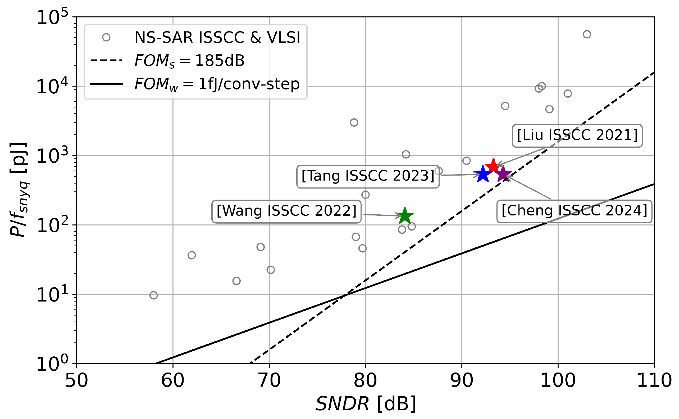
1. Introduction
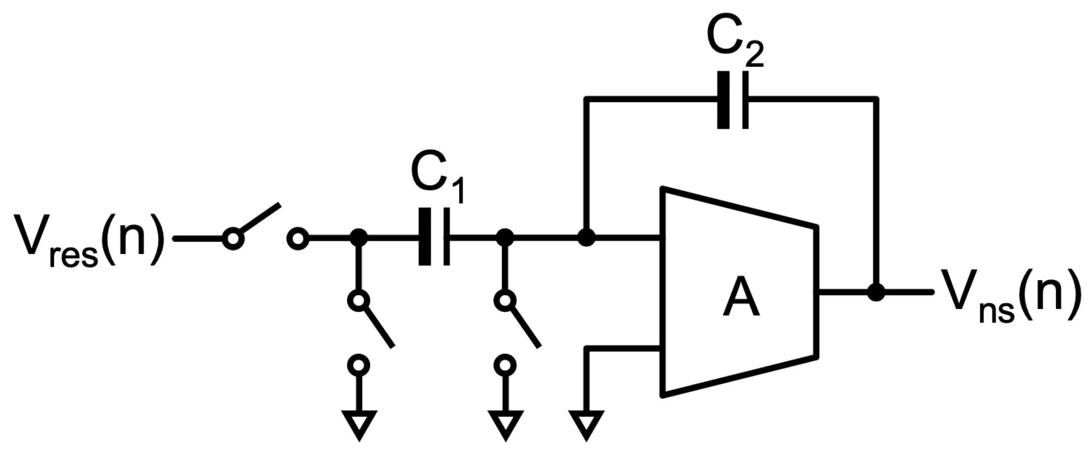
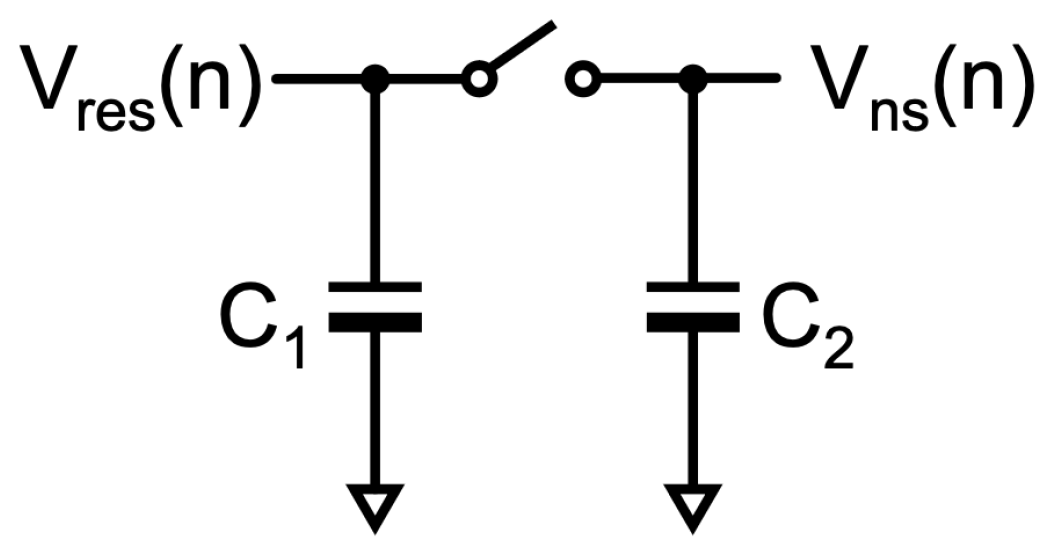
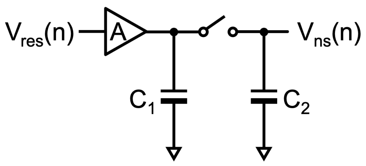
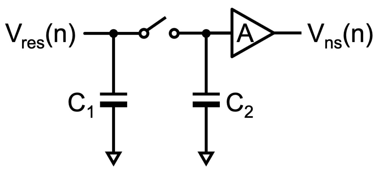
2. Principle of Integrator with Capacitor Stacking and Buffering
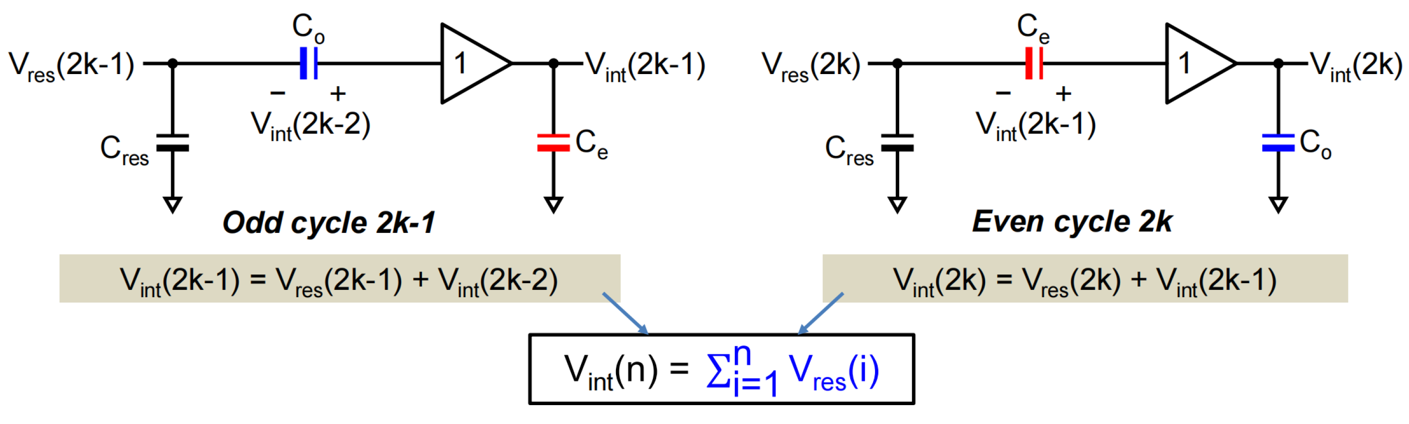
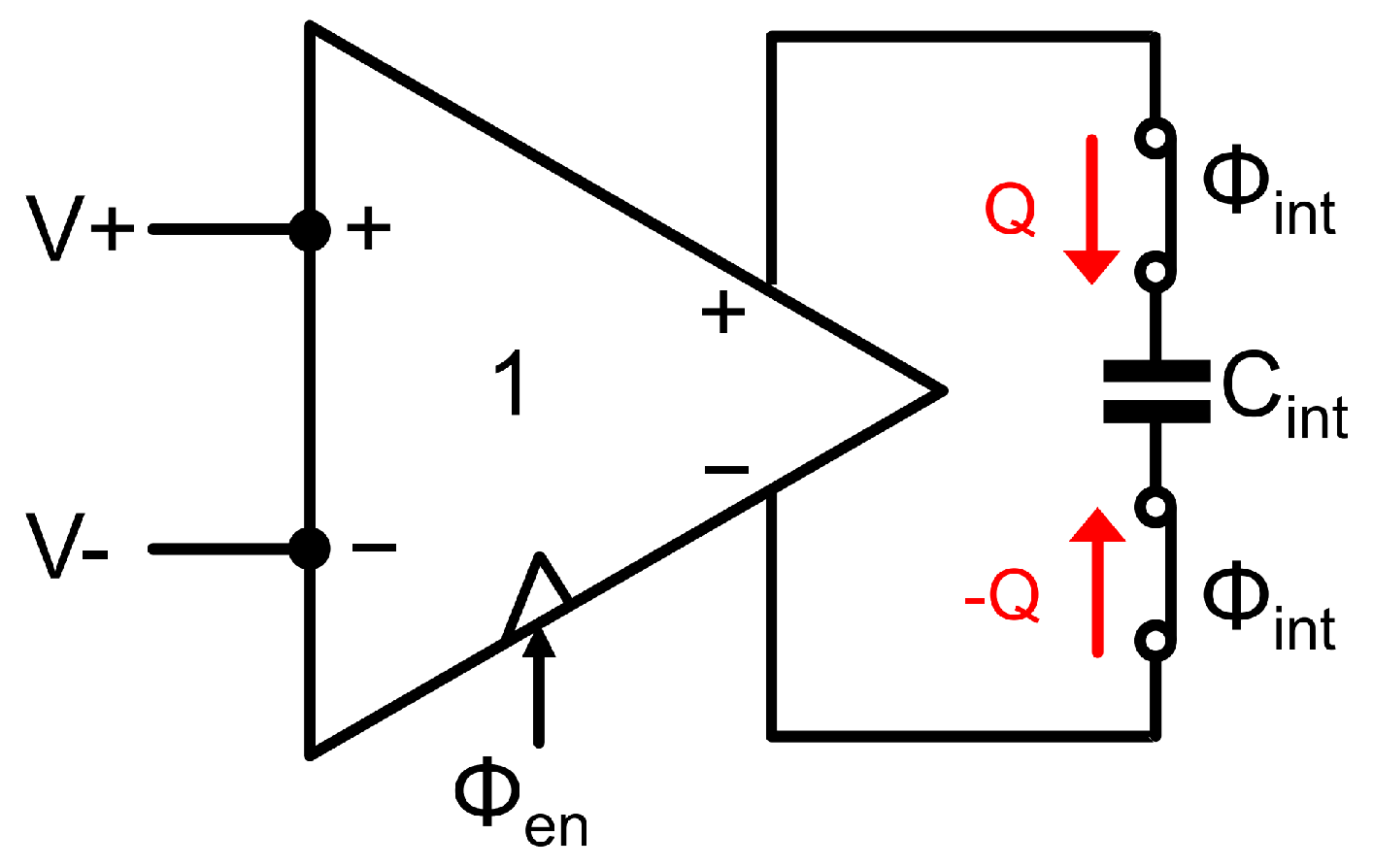
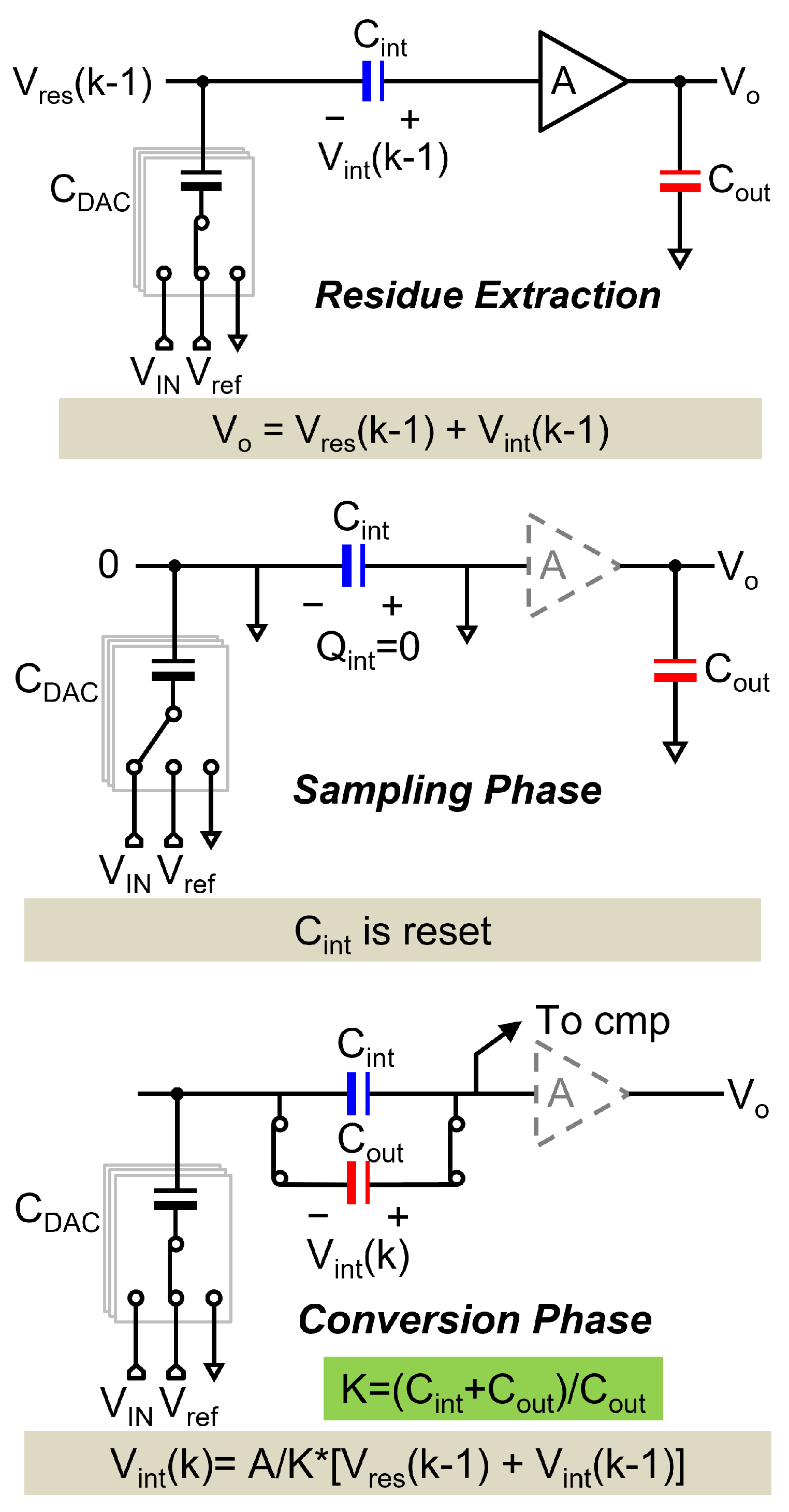
2.1. One-Time Integration
2.2. Continual Integration
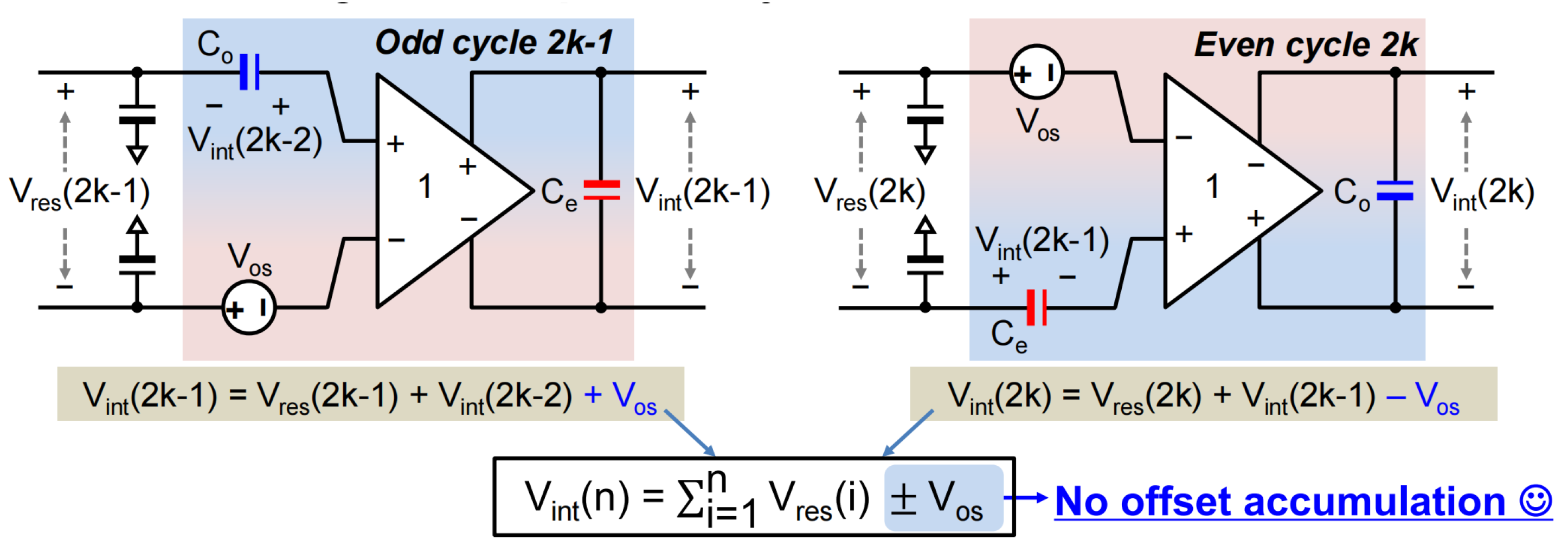
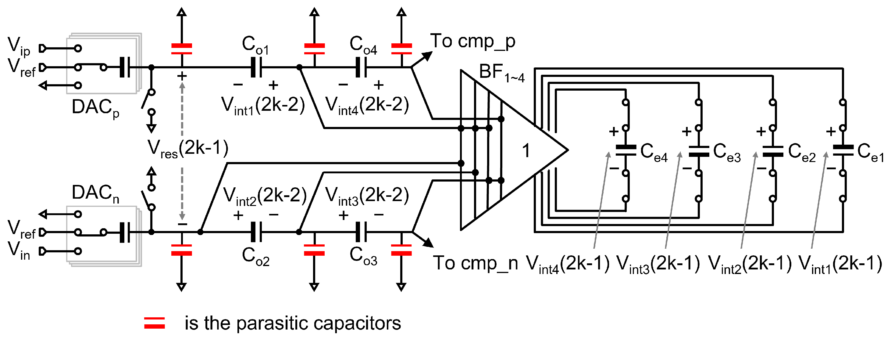
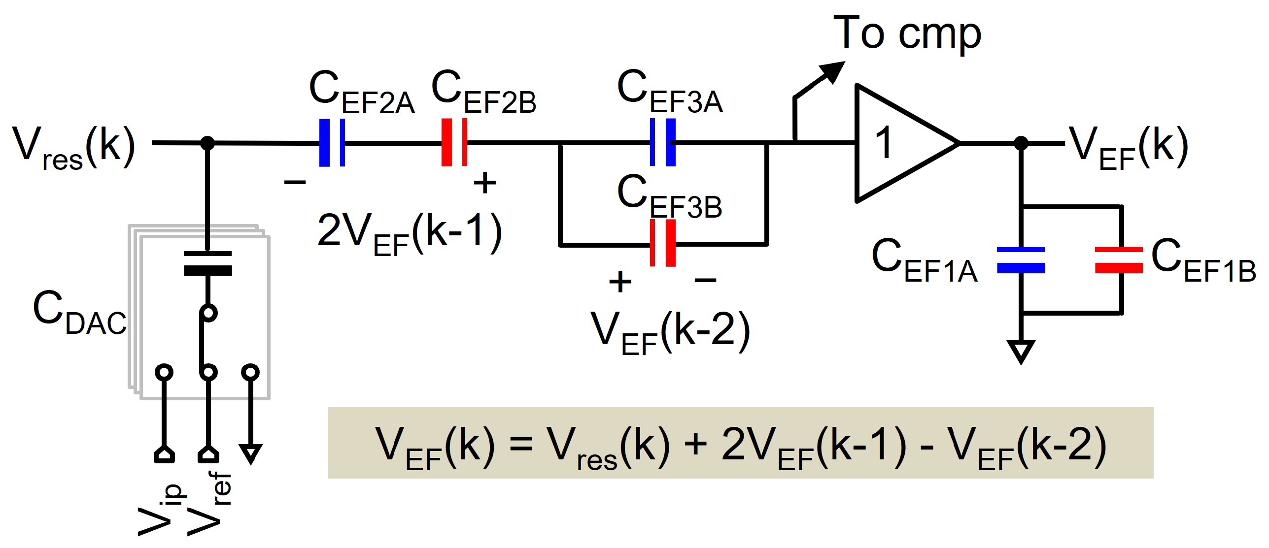
2.3. Differential Integration
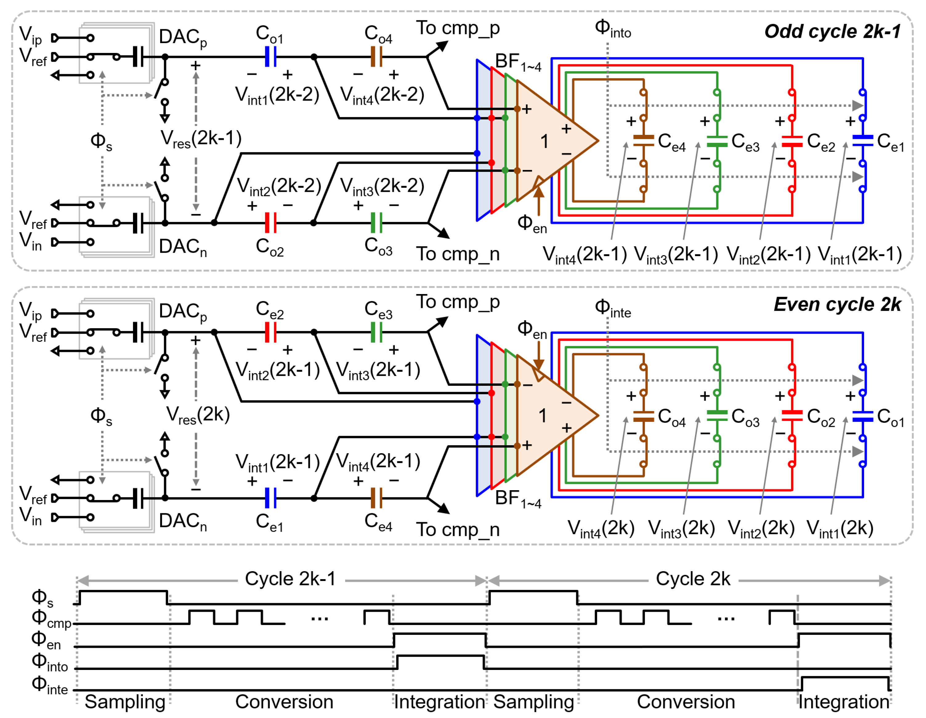
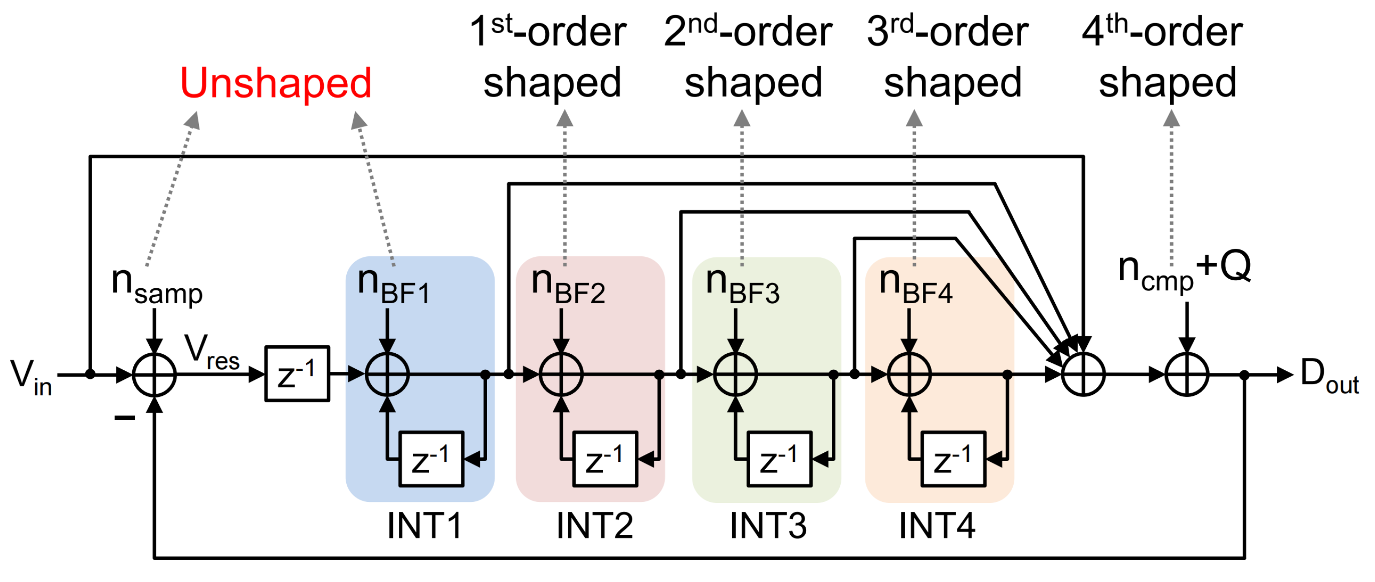
3. Noise-Shaping SAR ADC with CSB Integrator
4. Design Consideration and Circuit Implementation
4.1. The Parasitic Capacitance from Capacitor Stacking
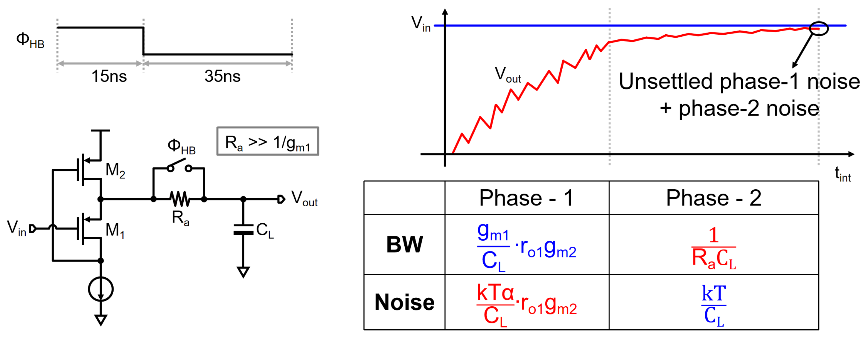
4.2. Non-Idealities from Switches
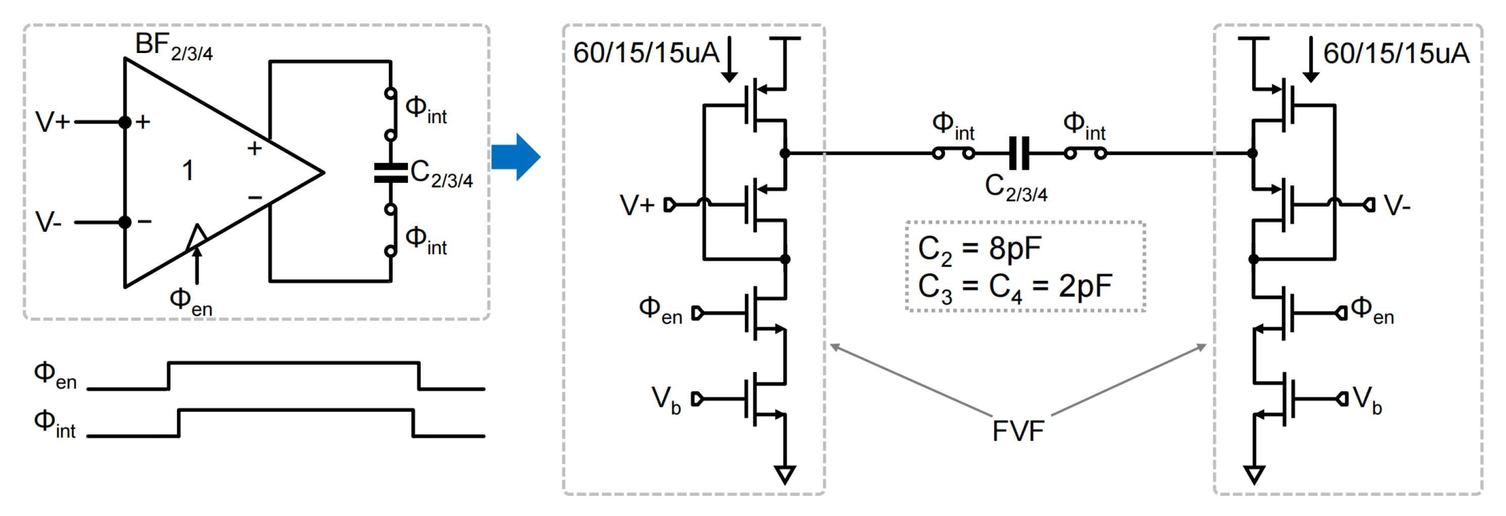
4.3. Integrator Design
4.4. Buffer Design
5. Conclusions
Author Contributions
Funding
Institutional Review Board Statement
Informed Consent Statement
Data Availability Statement
Conflicts of Interest
References
- Fredenburg, J.; Flynn, M. A 90 MS/s 11 MHz bandwidth 62dB SNDR noise-shaping SAR ADC. In Proceedings of the 2012 IEEE International Solid-State Circuits Conference (ISSCC), San Francisco, CA, USA, 19–23 February 2012; pp. 468–470. [Google Scholar] [CrossRef]
- Shu, Y.S.; Kuo, L.T.; Lo, T.Y. 27.2 an oversampling SAR ADC with DAC mismatch error shaping achieving 105 dB SFDR and 101 dB SNDR over 1 kHz BW in 55 nm CMOS. In Proceedings of the 2016 IEEE International Solid-State Circuits Conference (ISSCC), San Francisco, CA, USA, 31 January–4 February 2016; pp. 458–459. [Google Scholar] [CrossRef]
- Tang, X.; Yang, X.; Zhao, W.; Hsu, C.K.; Liu, J.; Shen, L.; Mukherjee, A.; Shi, W.; Pan, D.Z.; Sun, N. 9.5 A 13.5b-ENOB Second-Order Noise-Shaping SAR with PVT-Robust Closed-Loop Dynamic Amplifier. In Proceedings of the 2020 IEEE International Solid-State Circuits Conference—(ISSCC), San Francisco, CA, USA, 16–20 February 2020; pp. 162–164. [Google Scholar] [CrossRef]
- Obata, K.; Matsukawa, K.; Miki, T.; Tsukamoto, Y.; Sushihara, K. A 97.99 dB SNDR, 2 kHz BW, 37.1 μW noise-shaping SAR ADC with dynamic element matching and modulation dither effect. In Proceedings of the 2016 IEEE Symposium on VLSI Circuits (VLSI-Circuits), Honolulu, HI, USA, 15–17 June 2016; pp. 1–2. [Google Scholar] [CrossRef]
- Chen, Z.; Miyahara, M.; Matsuzawa, A. A 9.35-ENOB, 14.8 fJ/conv.-step fully-passive noise-shaping SAR ADC. In Proceedings of the 2015 Symposium on VLSI Circuits (VLSI Circuits), Kyoto, Japan, 16–18 June 2015; pp. C64–C65. [Google Scholar] [CrossRef]
- Guo, W.; Sun, N. A 12b-ENOB 61 μW noise-shaping SAR ADC with a passive integrator. In Proceedings of the ESSCIRC Conference 2016: 42nd European Solid-State Circuits Conference, Lausanne, Switzerland, 12–15 September 2016; pp. 405–408. [Google Scholar] [CrossRef]
- Lin, Y.Z.; Tsai, C.H.; Tsou, S.C.; Chu, R.X.; Lu, C.H. A 2.4-mW 25-MHz BW 300-MS/s passive noise shaping SAR ADC with noise quantizer technique in 14-nm CMOS. In Proceedings of the 2017 Symposium on VLSI Circuits, Kyoto, Japan, 5–9 June 2017; pp. C234–C235. [Google Scholar] [CrossRef]
- Li, S.; Qiao, B.; Gandara, M.; Sun, N. A 13-ENOB 2nd-order noise-shaping SAR ADC realizing optimized NTF zeros using an error-feedback structure. In Proceedings of the 2018 IEEE International Solid-State Circuits Conference (ISSCC), San Francisco, CA, USA, 11–15 February 2018; pp. 234–236. [Google Scholar] [CrossRef]
- Jie, L.; Zheng, B.; Chen, H.W.; Wang, R.; Flynn, M.P. 9.4 A 4th-Order Cascaded-Noise-Shaping SAR ADC with 88dB SNDR Over 100 kHz Bandwidth. In Proceedings of the 2020 IEEE International Solid-State Circuits Conference (ISSCC), San Francisco, CA, USA, 16–20 February 2020; pp. 160–162. [Google Scholar] [CrossRef]
- Liu, C.C.; Huang, M.C. 28.1 A 0.46 mW 5 MHz-BW 79.7 dB-SNDR noise-shaping SAR ADC with dynamic-amplifier-based FIR-IIR filter. In Proceedings of the 2017 IEEE International Solid-State Circuits Conference (ISSCC), San Francisco, CA, USA, 5–9 February 2017; pp. 466–467. [Google Scholar] [CrossRef]
- Miyahara, M.; Matsuzawa, A. An 84 dB dynamic range 62.5–625 kHz bandwidth clock-scalable noise-shaping SAR ADC with open-loop integrator using dynamic amplifier. In Proceedings of the 2017 IEEE Custom Integrated Circuits Conference (CICC), Austin, TX, USA, 30 April–3 May 2017; pp. 1–4. [Google Scholar] [CrossRef]
- Chen, Z.; Miyahara, M.; Matsuzawa, A. A 2nd order fully-passive noise-shaping SAR ADC with embedded passive gain. In Proceedings of the 2016 IEEE Asian Solid-State Circuits Conference (A-SSCC), Toyama, Japan, 7–9 November 2016; pp. 309–312. [Google Scholar] [CrossRef]
- Lin, Y.Z.; Lin, C.Y.; Tsou, S.C.; Tsai, C.H.; Lu, C.H. 20.2 A 40 MHz-BW 320 MS/s Passive Noise-Shaping SAR ADC With Passive Signal-Residue Summation in 14 nm FinFET. In Proceedings of the 2019 IEEE International Solid-State Circuits Conference (ISSCC), San Francisco, CA, USA, 17–21 February 2019; pp. 330–332. [Google Scholar] [CrossRef]
- Liu, J.; Wang, X.; Gao, Z.; Zhan, M.; Tang, X.; Sun, N. 9.3 A 40 kHz-BW 90 dB-SNDR Noise-Shaping SAR with 4× Passive Gain and 2nd-Order Mismatch Error Shaping. In Proceedings of the 2020 IEEE International Solid-State Circuits Conference (ISSCC), San Francisco, CA, USA, 16–20 February 2020; pp. 158–160. [Google Scholar] [CrossRef]
- Liu, J.; Li, S.; Guo, W.; Wen, G.; Sun, N. A 0.029-mm2 17-fJ/Conversion-Step Third-Order CT ΔΣ ADC with a Single OTA and Second-Order Noise-Shaping SAR Quantizer. IEEE J. Solid-State Circuits 2019, 54, 428–440. [Google Scholar] [CrossRef]
- Liu, J.; Li, D.; Zhong, Y.; Tang, X.; Sun, N. 27.1 A 250 kHz-BW 93 dB-SNDR 4th-Order Noise-Shaping SAR Using Capacitor Stacking and Dynamic Buffering. In Proceedings of the 2021 IEEE International Solid-State Circuits Conference (ISSCC), San Francisco, CA, USA, 13–22 February 2021; Volume 64, pp. 369–371. [Google Scholar] [CrossRef]
- Cheng, K.C.; Chang, S.J.; Chen, C.C.; Hung, S.H. 9.7 A 94.3 dB SNDR 184 dB FoMs 4th-Order Noise-Shaping SAR ADC with Dynamic-Amplifier-Assisted Cascaded Integrator. In Proceedings of the 2024 IEEE International Solid-State Circuits Conference (ISSCC), San Francisco, CA, USA, 18–22 February 2024; Volume 67, pp. 180–182. [Google Scholar] [CrossRef]
- Wang, Z.; Jie, L.; Kong, Z.; Zhan, M.; Zhong, Y.; Wang, Y.; Tang, X. 10.6 A 150 kHz-BW 15-ENOB Incremental Zoom ADC with Skipped Sampling and Single Buffer Embedded Noise-Shaping SAR Quantizer. In Proceedings of the 2023 IEEE International Solid-State Circuits Conference (ISSCC), San Francisco, CA, USA, 19–23 February 2023; pp. 9–11. [Google Scholar] [CrossRef]
- Wang, T.; Xie, T.; Liu, Z.; Li, S. An 84 dB-SNDR Low-OSR 4th-Order Noise-Shaping SAR with an FIA-Assisted EF-CRFF Structure and Noise-Mitigated Push-Pull Buffer-in-Loop Technique. In Proceedings of the 2022 IEEE International Solid-State Circuits Conference (ISSCC), San Francisco, CA, USA, 20–26 February 2022; Volume 65, pp. 418–420. [Google Scholar] [CrossRef]
- Murmann, B. ADC Performance Survey 1997–2024. Available online: https://github.com/bmurmann/ADC-survey (accessed on 5 August 2024).
- Jie, L.; Tang, X.; Liu, J.; Shen, L.; Li, S.; Sun, N.; Flynn, M.P. An Overview of Noise-Shaping SAR ADC: From Fundamentals to the Frontier. IEEE Open J. Solid-State Circuits Soc. 2021, 1, 149–161. [Google Scholar] [CrossRef]
- Li, H.; Shen, Y.; Xin, H.; Cantatore, E.; Harpe, P. A 7.3-μ W 13-ENOB 98-dB SFDR Noise-Shaping SAR ADC With Duty-Cycled Amplifier and Mismatch Error Shaping. IEEE J. Solid-State Circuits 2022, 57, 2078–2089. [Google Scholar] [CrossRef]
- Yi, P.; Liang, Y.; Liu, S.; Xu, N.; Fang, L.; Hao, Y. A 625 kHz-BW, 79.3 dB-SNDR Second-Order Noise-Shaping SAR ADC Using High-Efficiency Error-Feedback Structure. IEEE Trans. Circuits Syst. II Express Briefs 2022, 69, 859–863. [Google Scholar] [CrossRef]


| ISSCC 16 Shu [2] | ISSCC 17 Liu [10] | ISSCC 20 Liu [14] | ISSCC 20 Tang [3] | ISSCC 20 Jie [9] | ISSCC 22 Wang [19] | ISSCC 23 Wang [18] | ISSCC 24 Cheng [17] | ISSCC 21 Liu [16] | |
|---|---|---|---|---|---|---|---|---|---|
| Process | 55 nm | 28 nm | 40 nm | 40 nm | 28 nm | 65 nm | 28 nm | 28 nm | 40 nm |
| NS Technique | Closed-loop OTA | Open-loop DA | CS 1 | Closed-loop DA | Open-loop amp. | Cap stack. 2 & DA & CS | Cap stack. & dynamic buffering & Passive gain | Cap stack. & DA & Passive gain | Cap stack. & dynamic buffering |
| NS Order | 1 | 1 | 1 | 2 | 4 | 4 | 2 | 4 | 4 |
| Sharp NTF Across PVT | Yes | No | No | Yes | No | Yes | Yes | Yes | Yes |
| Supply (V) | 1.2 | 1 | 1.1 | 1.1 | 1 | 1.2/2 | 2 | 1 | 1.1 |
| Area (mm2) | 0.072 | 0.0049 | 0.061 | 0.037 | 0.02 | 0.075 | 0.026 | 0.09 | 0.094 |
| (MS/s) | 1 | 132 | 2 | 10 | 2 | 5 | 2.4 | 5 | 5 |
| Power (μW) | 15.7 | 460 | 67.4 | 107 | 120 | 73.8/133.88 3 | 160 | 107.38 | 340 |
| OSR | 500 | 13.2 | 25 | 8 | 10 | 5 | 8 | 25 | 10 |
| BW (kHz) | 1 | 5000 | 40 | 625 | 100 | 500 | 150 | 100 | 250 |
| SNDR (dB) | 101 | 79.7 | 90.5 | 83.8 | 87.6 | 84.1 | 92.5 | 94.3 | 93.3 |
| DR (dB) | 101.7 | 81.8 | 94.3 | 85.5 | 89 | 84.9 | 93.9 | 94.6 | 95 |
| 4 (dB) | 178.9 | 180.1 | 178.2 | 181.5 | 176.8 | 182.4/180 3 | 182.2 | 184 | 182 |
Disclaimer/Publisher’s Note: The statements, opinions and data contained in all publications are solely those of the individual author(s) and contributor(s) and not of MDPI and/or the editor(s). MDPI and/or the editor(s) disclaim responsibility for any injury to people or property resulting from any ideas, methods, instructions or products referred to in the content. |
© 2024 by the authors. Licensee MDPI, Basel, Switzerland. This article is an open access article distributed under the terms and conditions of the Creative Commons Attribution (CC BY) license (https://creativecommons.org/licenses/by/4.0/).
Share and Cite
Shen, Z.; Yang, S.; Liu, J. Analysis and Design of Noise-Shaping SAR ADC with Capacitor Stacking and Buffering. Chips 2024, 3, 296-310. https://doi.org/10.3390/chips3040015
Shen Z, Yang S, Liu J. Analysis and Design of Noise-Shaping SAR ADC with Capacitor Stacking and Buffering. Chips. 2024; 3(4):296-310. https://doi.org/10.3390/chips3040015
Chicago/Turabian StyleShen, Zhaoyang, Shiheng Yang, and Jiaxin Liu. 2024. "Analysis and Design of Noise-Shaping SAR ADC with Capacitor Stacking and Buffering" Chips 3, no. 4: 296-310. https://doi.org/10.3390/chips3040015
APA StyleShen, Z., Yang, S., & Liu, J. (2024). Analysis and Design of Noise-Shaping SAR ADC with Capacitor Stacking and Buffering. Chips, 3(4), 296-310. https://doi.org/10.3390/chips3040015