SWA: SoftWare for Analog Design Automation

Abstract
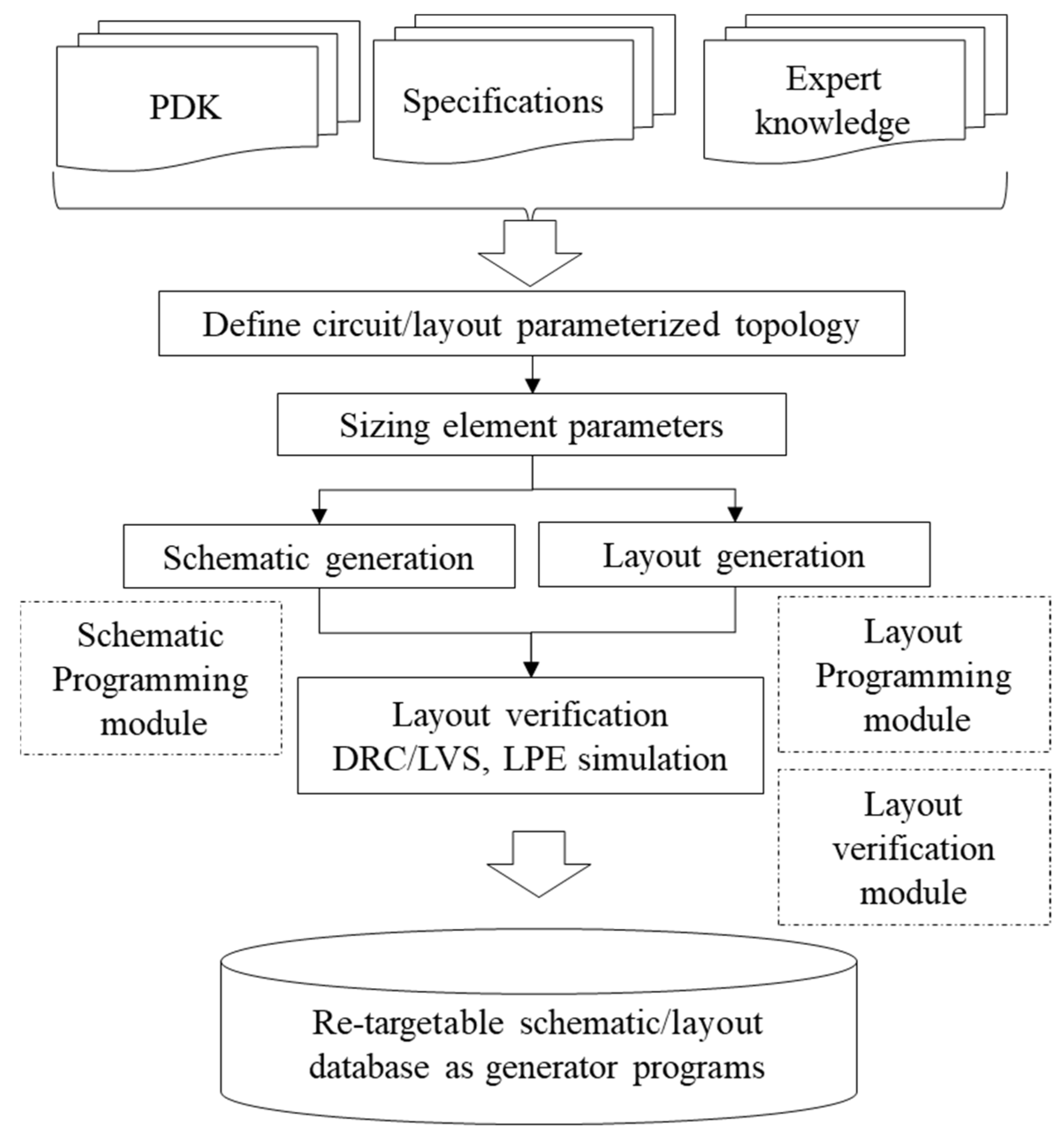
1. Introduction
2. SWA Overview
2.1. SWA Basics
| Listing 1. SWA program skeleton. |
| 1 Procedure( Cell_A(libName cellName ) |
| 2 Cell_A_layout(libName cellName “layout”) |
| 3 Cell_A_schematic(libName cellName “symbol”) |
| 4 Cell_A_symbol(libName cellName “schematic”) |
| 5 ) |
| 6 Procedure( Cell_A_layout(lib cell view) |
| 7 cv = SWA_CheckOpen(lib cell view techfile) |
| 8 LAY = SWA_list( |
| 9 list( “%pin” “VDD” “inputOutput” “m1” 0:10 …) |
| 10 list( “%pInst” “mylib” “mycell” “layout” “M0” …) |
| 11 list( “%path” “m1” 0:10 …) |
| 12 ... |
| 13 ) |
| 14 SWA_layTrans(cv LAY list(“R0” ‘(0 0))) |
| 15 save(cv) |
| 16 SWA_AUTOPVS_run_drc(…) |
| 17 SWA_AUTOPVS_run_lvs(…) |
| 18 close(cv) |
| 19 ) |
| 20 Procedure( Cell_A_schematic( lib cell view) |
| 21 cv = SWA_CheckOpen( lib cell view techfile) |
| 22 CKT = SWA_list( |
| 23 list(“%pin” “analogLib” “sympin” “symbol” “inputOutput” “VDD”…) |
| 24 list(“%pInst” “mylib” “nch” “symbol” “M1” 2:10 …) |
| 25 list(“VDD” 2:10 ) |
| 26 … |
| 27 ) |
| 28 SWA_sch( cv CKT ) |
| 29 check( cv) |
| 30 save(cv) |
| 31 close(cv) |
| 32 ) |
| 33 Procedure( Cell_A_symbol( lib cell view ) |
| 34 … |
| 34 ) |
| 35 Procedure( Process_Change() |
| 37 ;; Define layout grid, layer usage, width and spacing rules |
| 38 ;; for process compatibility |
| 39 ) |
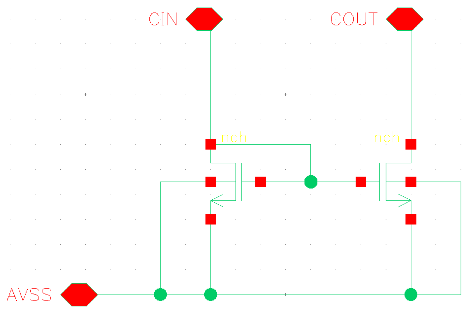
| Listing 2. SWA commands for Figure 2 example schematic. |
| 1 cirmirSch = SWA_list( |
| 2 (“%pin” “AVSS” “inputOutput” 0.0:0.0 “R0” nil) |
| 3 (“%pin” “CIN” “inputOutput” 5.0:11.0 “R0” nil) |
| 4 (“%pin” “COUT” “inputOutput” 13.0:11.0 “R0” nil) |
| 5 (“%pInst” “myLib” “nch” “symbol” “M1” 7.0:4.5 “MY” |
| ‘((“W” “string” “0.3u”) (“1” “string” “65n”) (“fingers” “string” “2”))) |
| 6 (“%pInst” “myLib” “nch” “symbol” “M2” 11.0:4.5 “R0” |
| ‘((“W” “string” “0.3u”) (“1” “string” “65n”) (“fingers” “string” “2”))) |
| 7 (“” list(0.0:0.0 5.0:0.0) 0) |
| 8 (“” list(5.0:0.0 5.0:3.0) 0) |
| 9 (“” list(5.0:4.5 3.0:4.5) 0) |
| 10 (“” list(3.0:4.5 3.0:0.0) 0) |
| 11 (“” list(7.0:4.5 11.0:4.5) 0) |
| 12 (“” list(7.0:4.5 9.0:4.5) 0) |
| 13 (“” list(9.0:4.5 9.0:6.0) 0) |
| 14 (“” list(9.0:6.0 5.0:6.0) 0) |
| 15 (“” list(0.0:0.0 13.0:0.0) 0) |
| 16 (“” list(13.0:0.0 13.0:3.0) 0) |
| 17 (“” list(13.0:4.5 15.0:4.5) 0) |
| 18 (“” list(15.0:4.5 15.0:0.0) 0) |
| 19 (“” list(15.0:0.0 13.0:0.0) 0) |
| 20 (“” list(5.0:6.0 5.0:11.0) 0) |
| 21 (“” list(13.0:6.0 13.0:11.0) 0) |
| 22 ) |
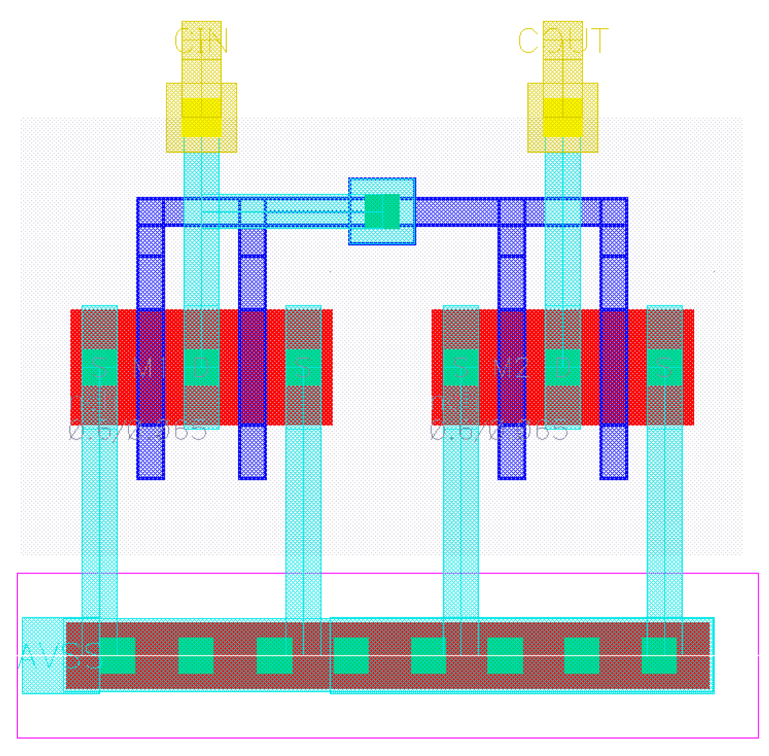
| Listing 3. SWA commands for Figure 3 example layout. |
| 1 curmirLay = SWA_list( |
| 2 (“%pInst” “myLib” “nch” “layout” “M1” 0.5:0.6 “R0” |
| ‘((“W” “string” “0.3u”) (“1” “string” “65n”) (“fingers” “string” “2”))) |
| 3 (“%pInst” “myLib” “nch” “layout” “M2” 1.44:0.6 “R0” |
| ‘((“W” “string” “0.3u”) (“1” “string” “65n”) (“fingers” “string” “2”))) |
| 4 (“%pin” “AVSS” “inputOutput” “M1” 0.3:0.0 0.2 “centerCenter” “R0” 0.0625) |
| 5 (“%path1” “M1” list(1.0:0.0 2.0:0.0) 0.2) |
| 6 (“%path1” “M1” list(0.4:0.75 0.4:0.0) 0.09) |
| 7 (“%path1” “M1” list(0.93:0.75 0.93:0.0) 0.09) |
| 8 (“%path1” “M1” list(1.34:0.75 1.34:0.0) 0.09) |
| 9 (“%path1” “M1” list(1.87:0.75 1.87:0.0) 0.09) |
| 10 (“%pin” “CIN” “inputOutput” “M2” 0.665:1.6 0.1 “centerCenter” “R0” 0.0625) |
| 11 (“%path1” “M1” list(0.665:0.75 0.665:1.4) 0.09) |
| 12 (“%via1” “M2_M1”0.665:1.4 “R0” ‘((“cutColumns” 1) (“cutRows” 1) |
| (“cutSpacing” (0.13 0.13)) (“layer1Enc” (0.04 0.04)) (“layer2Enc” (0.04 0.04)))) |
| 13 (“%path1” “M2” list(0.665:1.4 0.665:1.6) 0.09) |
| 14 (“%pin” “COUT” “inputOutput” “M2” 1.605:1.6 0.1 “centerCenter” “R0” 0.0625) |
| 15 (“%path1” “M1” list(1.605:0.75 1.605:1.4) 0.09) |
| 16 (“%via1” “M2_M1”1.605:1.4 “R0” ‘((“cutColumns” 1) (“cutRows” 1) |
| (“cutSpacing” (0.13 0.13)) (“layer1Enc” (0.04 0.04)) (“layer2Enc” (0.04 0.04)))) |
| 17 (“%path1” “M2” list(1.605:1.4 1.605:1.6) 0.09) |
| 18 (“rect1” “PO” 0.5:1.04 0.565:1.19) |
| 19 (“rect1” “PO” 0.765:1.04 0.83:1.19) |
| 20 (“rect1” “PO” 1.44:1.04 1.505:1.19) |
| 21 (“rect1” “PO” 1.705:1.04 1.77:1.19) |
| 22 (“rect1” “PO” (0.5 1.19) (1.77 1.12)) |
| 23 (“%path1” “PO” list(0.83:1.155 1.135:1.155) 0.07) |
| 24 (“%via1” “M1_PO” 1.135:1.155 “R0” ‘((“cutColumns” 1) (“cutRows” 1) |
| (“cutSpacing” (0.14 0.14)) (“layer1Enc” (0.04 0.04)) (“layer2Enc” (0.04 0.04)))) |
| 25 (“%path1” “M1” list(1.135:1.155 0.665:1.155) 0.07) |
| 26 (“%guardring” “PSubGuardring” nil 0.4:0.0 2.0:0.0 1.9:0.0) |
| 27 (“rect1” “NP” 0.195:0.26 2.075:1.4) |
| 28 ) |
| Listing 4. Conventional programming for Figure 3 example layout. |
| 1 techVia = FindViaByName(getTechFile(cv) “M2_M1”) |
| 2 createVia(cv techVia 0.665:1.4 “R0” ’((“cutSpacing” (0.130 0.130)))) |
| 3 createVia(cv techVia 1.605:1.4 “R0” ’((“cutSpacing” (0.130 0.130)))) |
| 4 techViaPO = FindViaByName(getTechFile(cv) “M1_PO”) |
| 5 createVia(cv techViaPO 1.135:1.155 “R0” ’((“cutSpacing” (0.140 0.140)))) |
| 6 ;; |
| 7 createPath(cv list(“PO” “drawing”) list(0.83:1.155 1.135:1.155) 0.07 “truncateExtend”) |
| 8 createRect(cv list(“PO” “drawing”) list(0.5:1.12 1.77:1.19)) |
| 9 createRect(cv list(“PO” “drawing”) list(1.705:1.04 1.77:1.19)) |
| 10 createRect(cv list(“PO” “drawing”) list(1.440:1.04 1.505:1.19)) |
| 11 createRect(cv list(“PO” “drawing”) list(0.765:1.04 0.83:1.19)) |
| 12 createRect(cv list(“PO” “drawing”) list(0.5:1.040 0.565:1.19)) |
| 13 createPath(cv list("OD" “drawing”) list(0.4:0.0 1.9:0.0) 0.17 “extendExtend”) |
| 14 createPath(cv list(“M1” “drawing”) list(0.4:0.0 1.9:0.0) 0.19 “extendExtend”) |
| 15 createPath(cv list(“M1” “drawing”) list(1.135:1.155 0.665:1.155) 0.09 “truncateExtend”) |
| 16 createPath(cv list(“M1” “drawing”) list(1.605:0.75 1.605:1.4) 0.09 “truncateExtend”) |
| 17 createPath(cv list(“M1” “drawing”) list(0.665:0.75 0.665:1.4) 0.09 “truncateExtend”) |
| 18 createPath(cv list(“M1” “drawing”) list(1.87:0.75 1.87:0.0) 0.09 “truncateExtend”) |
| 19 createPath(cv list(“M1” “drawing”) list(1.34:0.75 1.34:0.0) 0.09 “truncateExtend”) |
| 20 createPath(cv list(“M1” “drawing”) list(0.93:0.75 0.93:0.0) 0.09 “truncateExtend”) |
| 21 createPath(cv list(“M1” “drawing”) list(0.4:0.75 0.4:0.0) 0.09 “truncateExtend”) |
| 22 createPath(cv list(“M1” “drawing”) list(1.0:0.0 2.0:0.0) 0.2 “truncateExtend”) |
| 23 pinAVSS = createRect(cv list(“M1” “drawing”) list(0.2:-0.1 0.4:0.1)) |
| 24 createRect(cv list("CO" “drawing”) list(1.81:-0.045 1.9:0.045)) |
| 25 createRect(cv list("CO" “drawing”) list(1.61:-0.045 1.7:0.045)) |
| 26 createRect(cv list("CO" “drawing”) list(1.41:-0.045 1.5:0.045)) |
| 27 createRect(cv list("CO" “drawing”) list(1.21:-0.045 1.3:0.045)) |
| 28 createRect(cv list("CO" “drawing”) list(1.01:-0.045 1.1:0.045)) |
| 29 createRect(cv list("CO" “drawing”) list(0.81:-0.045 0.9:0.045)) |
| 30 createRect(cv list("CO" “drawing”) list(0.605:-0.045 0.695:0.045)) |
| 31 createRect(cv list("CO" “drawing”) list(0.40:-0.045 0.49:0.045)) |
| 32 pin_CIN = createRect(cv list(“NP” “drawing”) list(0.195:0.26 2.075:1.4)) |
| 33 label = createLabel(cv list(“M1” “pin”) 0.3:0.0 “AVSS” “centerCenter” “R0” “stick” 0.063) |
| 34 createPath(cv list(“M2” “drawing”) list(1.605:1.40 1.605:1.6) 0.1 “truncateExtend”) |
| 35 pinCOUT = createRect(cv list(“M2” “drawing”) list(1.555:1.55 1.655:1.6 |
| 36 createPath(cv list(“M2” “drawing”) list(0.665:1.4 0.665:1.6) 0.1 “truncateExtend”) |
| 37 createRect(cv list(“M2” “drawing”) list(0.615:1.55 0.71:1.65)) |
| 38 label = createLabel(cv list(“M2” “pin”) 1.605:1.6 “COUT” “centerCenter” “R0” “stick” 0.063) |
| 39 label = createLabel(cv list(“M2” “pin”) 0.0665:1.6 “CIN” “centerCenter” “R0” “stick” 0.063) |
| 40 createPath(cv list("PP" “drawing”) list(0.4:0.0 1.9:0.0) 0.43 “extendExtend”) |
| 41 ;; |
| 42 nchSym = OpenCellView(“myLib” “nch” “layout”) |
| 43 nchM2 = createInst(cv nchSym “M2” 1.44:0.6 “R0” 0) |
| 44 createProp(nchM2 “W” “string” “300n”) |
| 45 createProp(nchM2 “1” “string” “65.0n”) |
| 46 createProp(nchM2 “fingers” “string” “2”) |
| 47 createInst(cv nchSym “M1” 0.5:0.6 “R0” 0) |
| 48 createProp(nchM1 “W” “string” “300n”) |
| 49 createProp(nchM1 “1” “string” “65.0n”) |
| 50 createProp(nchM1 “fingers” “string” “2”) |
| 51 ;; |
| 52 netAVSS = createNet(cv “AVSS” nil) |
| 53 netCIN = createNet(cv “CIN” nil) |
| 54 netCOUT = createNet(cv “COUT” nil) |
| 55 createTerm(netAVSS “AVSS” “inputOutput”) |
| 56 createTerm(netCIN “CIN” “inputOutput”) |
| 57 createTerm(netCOUT “COUT” “inputOutput”) |
| 58 createPin(netAVSS pinAVSS “AVSS”) |
| 59 createPin(netCIN pinCIN “CIN”) |
| 60 createPin(netCOUT pinCOUT “COUT”) |
2.2. SWA Macro Commands
| Listing 5. SWA macro command for Figure 2 example schematic. |
| 1 procedure( SWA_CURMIR_sch( lib cell view ) |
| 2 prog( (cv trProps cirmir) |
| 3 cv = SWA_CheckOpen( lib cell view SWA_techname ) |
| 4 trProps = list( |
| 5 ’(“W” “string” “0.3u”) ’(“1” “string” “65n”) ’(“fingers” “string” “2”) |
| 6 ) |
| 7 curmir = SWA_list( |
| 8 SWA_schPin( “AVSS” “inputOutput” 0.0:0.0 “R0” ) |
| 9 SWA_schPin( “CIN” “inputOutput” 5.0:11.0 “R0” ) |
| 10 SWA_schPin( “COUT” “inputOutput” 13.0:11.0 “R0” ) |
| 11 |
| 12 SWA_schPInst( “myLib” “nch” “symbol” “M1” 7.0:4.5 “MY” trProps ) |
| 13 SWA_schPInst( “myLib” “nch” “symbol” “M2” 11.0:4.5 “R0” trProps ) |
| 14 |
| 15 SWA_schWire( AVSS.xy “abs” xCoord(M1.S):0.0 “abs” M1.S ) |
| 16 SWA_schWire( M1.B -2.0:0 0.0:-4.5 ) |
| 17 SWA_schWire( M1.G “abs” M2.G ) |
| 18 SWA_schWire( M1.G 2.0:0.0 0.0:1.5 “abs” M1.D ) |
| 19 SWA_schWire( AVSS.xy “abs” xCoord(M2.S):0.0 “abs” M2.S ) |
| 20 SWA_schWire( M2.B 2.0:0 0.0:-4.5 -2.0:0.0) |
| 21 SWA_schWire( M1.D “abs” CIN.xy ) |
| 22 SWA_schWire( M2.D “abs” COUT.xy ) |
| 23 ) |
| 24 SWA_sch( cv curmir ) |
| 25 check( cv ) |
| 26 save( cv ) |
| 27 close( cv ) |
| 28 ) |
| 29 ) |
| Listing 6. SWA macro command for Figure 3 example layout. |
| 1 procedure( SWA_CURMIR_lay( lib cell view ) |
| 2 prog( (cv trProp cirmir) |
| 3 cv = SWA_CheckOpen( lib cell view SWA_techname ) |
| 4 trProps = list( |
| 5 ’(“W” “string” “0.3u”) ’(“1” “string” “65n”) ’(“fingers” “string” “2”) |
| 6 ) |
| 7 curmir = SWA_list( |
| 8 ;; M1 |
| 9 SWA_layAlignMOSPins( |
| 10 SWA_layPInst( cv “myLib” “nch” “layout” “M1” 0.5:0.6 “R0” trProps ) |
| 11 ) |
| 12 ;; M2 |
| 13 SWA_layAlignMOSPins( |
| 14 SWA_layPInst( cv “myLib” “nch” “layout” “M2” 1.44:0.6 “R0” trProps ) |
| 15 ) |
| 16 ;; AVSS |
| 17 SWA_layPin( “AVSS” “inputOutput” “M1” 0.3:0.0 0.2 ) |
| 18 SWA_layWire( “M1” 0.2 1.0:0.0 2.0:0.0 ) |
| 19 SWA_layWire( M1.SD0 xCoord(M1.SD0_xy):0.0 ) |
| 20 SWA_layWire( M1.SD2 xCoord(M1.SD2_xy):0.0 ) |
| 21 SWA_layWire( M2.SD0 xCoord(M2.SD0_xy):0.0 ) |
| 22 SWA_layWire( M2.SD2 xCoord(M2.SD2_xy):0.0 ) |
| 23 ;; CIN |
| 24 SWA_layPin( “CIN” “inputOutput” “M2” xCoord(M1.SD1_xy):1.6 0.10 ) |
| 25 SWA_layWire( M1.SD1 xCoord(M1.SD1_xy):1.4 “M2” CIN.xy ) |
| 26 ;; COUT |
| 27 SWA_layPin( “COUT” “inputOutput” “M2” xCoord(M2.SD1_xy):1.6 0.10 ) |
| 28 SWA_layWire( M2.SD1 xCoord(M2.SD1_xy):1.4 “M2” COUT.xy ) |
| 29 ;; Gate |
| 30 SWA_layRect( “PO” M1.G0_llx:M1.G0_ury M1.G0_urx:M1.G0_ury+0.15 ) |
| 31 SWA_layRect( “PO” M1.G1_llx:M1.G1_ury M1.G1_urx:M1.G1_ury+0.15 ) |
| 32 SWA_layRect( “PO” M2.G0_llx:M2.G0_ury M2.G0_urx:M2.G0_ury+0.15 ) |
| 33 SWA_layRect( “PO” M2.G1_llx:M2.G1_ury M2.G1_urx:M2.G1_ury+0.15 ) |
| 34 SWA_layRect( “PO” M1.G0_llx:M2.G1_ury+0.15 M2.G1_urx:M2.G1_ury+0.15-0.070 ) |
| 35 SWA_layWire( “PO” 0.07 M1.G1_urx:M1.G1_ury+0.15-0.035 |
| 36 1.135:M1.G1_ury+0.15-0.035 “M1” xCoord(M1.SD1_xy):M1.G1_ury+0.15-0.035 ) |
| 37 ;; SUB |
| 38 SWA_layGR(“PSubGuardring” nil 0.4:0.0 2.0:0.0 1.9:0.0) |
| 39 SWA_layRect( “NP” 0.195:0.26 2.075:1.4 ) |
| 40 ) |
| 41 SWA_layTrans( cv curmir list(0.0:0.0 “R0”) ) |
| 42 save( cv ) |
| 43 close( cv ) |
| 44 ) |
| 45 ) |
2.3. Layout Verification
3. Design Example
4. Discussion
5. Conclusions
Author Contributions
Funding
Institutional Review Board Statement
Informed Consent Statement
Data Availability Statement
Acknowledgments
Conflicts of Interest
References
- Accellera. Verilog-AMS language Reference Manual. Available online: https://www.accellera.org/images/downloads/standards/v-ams/VAMS-LRM-2-4.pdf (accessed on 1 November 2024).
- Synopsys, Inc. Python API Reference Manual. Available online: https://www.synopsys.com/cgi-bin/pycellstudio/req1.cgi (accessed on 1 November 2024).
- Cadence Design Systems, Inc. Virtuoso Parameterized Cell SKILL Reference: Commercial software product reference manual from Cadence Design Systems, Inc.
- Zhu, K.; Chen, H.; Liu, M.; Pan, D.Z. Tutorial and Perspectives on MAGICAL: A Silicon-Proven Open-Source Analog IC Layout System. IEEE Trans. Circuits Syst. II Express Briefs 2023, 70, 715–720. [Google Scholar] [CrossRef]
- Wu, P.H.; Lin, M.P.H.; Chen, T.C.; Yeh, C.F.; Li, X.; Ho, T.Y. A Novel Physical Synthesis Methodology Integrating Existent Design Expertise. IEEE Trans. Comput.-Aided Des. Integr. Circuits Syst. 2015, 34, 199–212. [Google Scholar] [CrossRef]
- Chen, H.; Zhu, K.; Liu, M.; Tang, X.; Sun, N.; Pan, D.Z. Toward Silicon-Proven Detailed Routing for Analog and Mixed-Signal Circuits. In Proceedings of the 39th International Conference on Computer-Aided Design, Virtual, 2–5 November 2020. [Google Scholar] [CrossRef]
- Zhu, K.; Chen, H.; Liu, M.; Tang, X.; Sun, N.; Pan, D.Z. Effective Analog/Mixed-Signal Circuit Placement Considering System Signal Flow. In Proceedings of the 39th International Conference on Computer-Aided Design, Virtual, 2–5 November 2020; Volume 133, pp. 1–9. [Google Scholar] [CrossRef]
- Xu, B.; Basaran, B.; Su, M.; Pan, D.Z. Analog Placement Constraint Extraction and Exploration with the Application to Layout Retargeting. In Proceedings of the 2018 International Symposium on Physical Design, Monterey, CA, USA, 25–28 March 2018; pp. 98–105. [Google Scholar] [CrossRef]
- Zhu, K.; Liu, M.; Lin, Y.; Hao, C. magical-eda/MAGICAL. Available online: https://github.com/magical-eda/MAGICAL (accessed on 1 November 2024).
- Chang, E.; Han, J.; Bae, W.; Wang, Z.; Narevsky, N.; Nikolic, B.; Alon, E. BAG2: A Process-portable framework for generator-based AMS circuit design. In Proceedings of the 2018 IEEE Custom Integrated Circuits Conference, San Diego, CA, USA, 8–11 April 2018; pp. 1–8. [Google Scholar] [CrossRef]
- ucb-art/BAG_framework: Berkeley Analog Generator (BAG). Available online: https://github.com/ucb-art/BAG_framework (accessed on 1 November 2024).
- Hakhamaneshi, K.; Werblun, N.; Abbeel, P.; Stojanovic, V. BagNet: Berkeley Analog Generator with Layout Optimizer Boosted with Deep Neural Networks. In Proceedings of the 2019 IEEE/ACM International Conference on Computer-Aided Design, Westminster, CO, USA, 4–7 November 2019; pp. 1–8. [Google Scholar] [CrossRef]
- Wang, Z.; Alon, E. Analog Generators for SerDes Clock Generation and Distribution, 2023, Technical Reports-2023, Electrical Engineering & Computer Sciences, Berkeley. Available online: https://www2.eecs.berkeley.edu/Pubs/TechRpts/2023/EECS-2023-36.pdf (accessed on 1 November 2024).
- Bio, M.; Scherr, W.; Agbemenu, A.S.; Sondón, S.M.; Hande, V.; Sturm, J. BAG2-assisted analog layout synthesis for TSMC 65nm and GPDK 45 nm. e+i Elektrotechnik Informationstechnik 2024, 141, 88–100. [Google Scholar] [CrossRef]
- Cadence Design Systems, Inc. SKILL Language User Guide: Commercial software product reference manual from Cadence Design Systems, Inc.
- Cadence Design Systems, Inc. SKILL Language Reference: Commercial software product reference manual from Cadence Design Systems, Inc.
- Cadence Design Systems, Inc. Virtuoso Design Environment SKILL Reference: Commercial software product reference manual from Cadence Design Systems, Inc.
- Cadence Design Systems, Inc. Virtuoso Layout Suite XL SKILL Reference: Commercial software product reference manual from Cadence Design Systems, Inc.
- Cadence Design Systems, Inc. Cadence Physical Verification System Developer Guide: Commercial software product reference manual from Cadence Design Systems, Inc.
- Cadence Design Systems, Inc. Assura Physical Verification User Guide: Commercial software product reference manual from Cadence Design Systems, Inc.
- Cadence Design Systems, Inc. Quantus Extraction User’s Manual: Commercial software product reference manual from Cadence Design Systems, Inc.
- Sugawara, M. A Study of Design Methodology for Mixed-Signal Circuits Using Sub-Micron Slice Structures. Ph.D. Thesis, Tokyo Institute of Technology, Meguro, Japan, Tokyo, Japan, 2019. [Google Scholar]
- Sugawara, M.; Mori, K.; Xu, Z.; Miyahara, M.; Okada, K.; Matsuzawa, A. Synthesis and Automatic Layout of Resistive Digital-to-Analog Converter Based on Mixed-Signal Slice Cell. IEICE Trans. Fundam. Electron. Commun. Comput. Sci. 2016, E99.A, 2435–2443. [Google Scholar] [CrossRef]
- Sugawara, M.; Mori, K.; Miyahara, M.; Matsuzawa, A. Novel Design Method for ~GHz DAC & Automated Design Program. Available online: https://www.ssc.pe.titech.ac.jp/private/publications/2014/IEEJ_AnalogRF/AnalogRF_sugawara_paper.pdf (accessed on 1 November 2024).
- Sugawara, M. METHOD FOR DESIGNING D/A CONVERTER EMBEDDED IN LSI. Japanese Patent Publication Number WO/2015/045187, Application Number PCT/JP2013/077873. Available online: https://patentscope2.wipo.int/search/ja/detail.jsf?docId=WO2015045187 (accessed on 1 November 2024).
- The Python Software Foundation, Python. Available online: https://www.python.org/ (accessed on 1 November 2024).
- John, K. Ousterhout, Tcl and the Tk Toolkit; Addison Wesley: Boston, MA, USA, 1994. [Google Scholar]
- Köfferlein, M. KLayout—Your Mask Layout Friend. Available online: https://www.klayout.de/ (accessed on 1 November 2024).
- PEARDROP DESIGN SYSTEMS, PEARDROP DESIGN SYSTEMS Affordable Analog Design. Available online: https://peardrop.co.uk/ (accessed on 1 November 2024).
- Cadence Design Systems, Inc. Cadence User Interface SKILL Reference: Commercial software product reference manual from Cadence Design Systems, Inc.
- Cadence Design Systems, Inc. Virtuoso Analog Environment L SKILL Reference: Commercial software product reference manual from Cadence Design Systems, Inc.
- Cadence Design Systems, Inc. Virtuoso Analog Design Environment XL SKILL Reference: Commercial software product reference manual from Cadence Design Systems, Inc.

| SWA Procedure | Function |
|---|---|
| SWA_CheckOpen( lib cell view tech ) | Create/clear cellview |
| SWA_list( list list … ) | Append command lists |
| SWA_sym( cv cmd_list ) | Symbol command interpreter |
| SWA_sch( cv cmd_list ) | Schematic command interpreter |
| SWA_layTrans( cv cmd_list [transform]) | Layout command interpreter |
| SWA_AUTOPVS_run_drc( libName cellName viewName drcRuleFiles ) | Run DRC |
| SWA_AUTOPVS_run_lvs( libName cellName viewName ruleFiles ) | Run LVS |
| SWA_AUTOASSURA_run_lvs( … ) | Run LVS for LPE |
| SWA_AUTOASSURA_run_qrc( … ) | Run LPE |
| Symbol Commands and Arguments | Function |
|---|---|
| list(“” type style pointList [width] ) | Draw symbol figure |
| list(“%box” [bBox] ) | Draw bounding box |
| list(“%pin” termName direction origin orient [labelSpec]) | Place pin |
| list(“%NoteLabel” origin labelText orient labelType [height]) | Place label |
| list(“%SymbolLabel” origin choice labelText orient labelType) | Place label with layer choice |
| Schematic command and arguments | Function |
| list(“%pin” termName direction origin orient [view]) | Place pin |
| list(“%inst” lib cell view name origin orient ) | Place instance |
| list(“%pInst” lib cell view name origin orient paramList ) | Place instance with parameters |
| list(labelText pointList labelOrigin [labelSpec] ) | Route wire with wire labelText |
| list(“%NoteLabel” origin labelText justify orient labelType height) | Place label |
| Layout command and arguments | Function |
| list(“%pin” name direction layer centerPoint width [labelSpec]) | Place layout pin |
| list(“%inst” lib cell view name name point orient) | Place instance |
| list(“%pInst” lib cell view name point orient paramList) | Place parameterized instance |
| list(“%path” layer point point … width) | Route wire |
| list(“%via” viaName point orient paramList) | Place Via |
| list(“%rect” layers bBox ) | Place rectangle |
| list(“%rect1” layer lowerLeft upperRight ) | Place rectangle |
| list(“%polygon” layer points ) | Place polygon |
| list(“%prBoundary” point point …) | Place boundary |
| list(“%guardRing” mppName isClosed point point …) | Place MPP guard ring |
| Schematic Macro Procedure Interface | Function |
|---|---|
| SWA_schPin( termName direction origin orient [view] ) | Place schematic termina/pin. |
| SWA_schPInst( libName cellName viewName name origin orient paramList ) | Place symbol instance with parameter specified. |
| SWA_schWire( startPoint (move|label)… ) | Route wire segments with the relative coordinate move. |
| SWA_schPin generated property | Property value |
| <termName>.xy | Terminal location in schematic, list(x y) |
| <pinName>.xy | Pin location in schematic, list(x y) |
| SWA_schInst generated property | Property value |
| <name>.<termName> | Terminal location in schematic, list(x y) |
| <name>.<pinName> | Pin location in schematic, list(x y) |
| Symbol Macro Procedure Interface | Function |
|---|---|
| SWA_symPin( termName direction origin orient [labelSpec] ) | Place symbol terminal/pin, optionally place pin label. |
| SWA_symShape( type [?style style] point point … ) | Draw a symbol figure. |
| SWA_symPin generated property | Property value |
| <termName>.xy | Terminal location, list(x y) |
| <pinName>.xy | Pin location, list(x y) |
| Layout Macro Procedure Interface | Function |
|---|---|
| SWA_layPin( termName direction layer origin [size [labelParameters]]) | Place layout pin. |
| SWA_layInst( libName cellName viewName name origin orient) | Place layout instance. |
| SWA_layPInst( cv libName cellName viewName name origin orient paramList) | Place layout PCell with parameters. |
| SWA_layWire( cmd0 cmd…) | Route wire segments allowing layer change with vias, and segment width change. |
| SWA_prBoundary( point point …) | Draw a bounding box. |
| SWA_layRect( layer point1 point2 [mode] ) | Draw rectangle. |
| SWA_layLabel( labelText layer origin [justify [orient [font [height]]]]) | Place text label. |
| SWA_layGR( mppName [closed] point…) | Draw an MPP guard ring. MPP setting is taken from the technology database. |
| SWA_layAlignMOSPins( SWA_layPInst command which places MOS PCell) | Place MOS PCell instance. Pin names are aligned from left to right, bottom to top. Ex. SD0, SD1, SD2, … |
| SWA_layPin Generated Property | Property Value |
|---|---|
| <termName | pinName>.lxy | list(layer centerXY pinBBox) |
| <termName | pinName>.layer | Layer of the pin |
| <termName | pinName>.xy | Pin center location, centerXY |
| <termName | pinName>.x | xCoord(centerXY) |
| <termName | pinName>.y | yCoord(centerXY) |
| <termName | pinName>.llx | xCoord(lowerLeft(pinBBox)) |
| <termName | pinName>.lly | yCoord(lowerLeft(pinBBox)) |
| <termName | pinName>.urx | xCoord(upperRight(pinBBox)) |
| <termName | pinName>.ury | yCoord(upperRight(pinBBox)) |
| <termName | pinName>.bBox | pinBBox |
| SWA_layInst generated property | Property value |
| <name>.<termName | pinName> | list(layer centerXY pinBBox) |
| <name>.<termName | pinName>_layer | Layer of the pin |
| <name>.<termName | pinName>_xy | Pin center location, centerXY |
| <name>.<termName | pinName>_x | xCoord(centerXY) |
| <name>.<termName | pinName>_y | yCoord(centerXY) |
| <name>.<termName | pinName>_llx | xCoord(lowerLeft(pinBBox)) |
| <name>.<termName | pinName>_lly | yCoord(lowerLeft(pinBBox)) |
| <name>.<termName | pinName>_urx | xCoord(upperRight(pinBBox)) |
| <name>.<termName | pinName>_ury | yCoord(upperRight(pinBBox)) |
| <name>.prBBox | Instance boundary |
| Layout | Conventional Programming | SWA Simple Command | SWA Macro Command |
|---|---|---|---|
| Place instance | Define place and route grid foreach instances; place instance using grid master=getCellView( lib cell “layout”) instance=createParameteriseInstance( cv master name origin orient parameterList) … ) | Define place and route grid. SWA_list( list (“%pInst” lib cell “layout” name origin orient parameterList) … ) | Optional: Define place and route grid SWA_list( SWA_layPInst (lib cell “layout” name origin orient parameterList) … ) |
| Place pin | foreach pins net1=createNet(pin_name1) term1 = createTerm(name1 name1) fig1=createRect(cv layer1 bBox1) createPin(net1 fig1 pin_name1 term1) … | SWA_list( list(“%pin” term1 direction1 layer1 point1 witdth1) … ) | SWA_list( SWA_layPin(term1 direction1 layer1 point1 width1) … ) |
| Route wire | foreach route createPath(cv firstLayer width point1 point2) createVia(cv viaName point2 orient viaParameter) createPath(cv secondLayer width1 point2 point3) createPath(cv secondLayer width2 point3 point4) … | SWA_list( list(“%path” firstLayer point1 point2 width) list(“%via” viaName point2 viaParameter) list(“%path” secondLayer point2 point3 width1) list(“%path” secondLayer point3 point4 width2) … ) | SWA_list( SWA_layWire(firstLayer width point1 point2 list(secondLayer viaName viaParameter) width1 point3 width2 point4 … ) ) |
| Type | Logic Tr. | Output Tr. | Resolution |
|---|---|---|---|
| 0 | 1.0 V core | 1.0 V core | 4–12 bit |
| 1 | 2.5 V under drive 1.8 V | 2.5 V under drive 1.8 V | 4–12 bit |
| 2 | 2.5 V | 2.5 V | 4–12 bit |
| 3 | 2.5 V overdrive 3.3 V | 2.5 V overdrive 3.3 V | 4–12 bit |
| 4 | 1.0 V core | 2.5 V under drive 1.8 V | 4–12 bit |
| 5 | 1.0 V core | 2.5 V | 4–12 bit |
| 6 | 1.0 V core | 2.5 V overdrive 3.3 V | 4–12 bit |
Disclaimer/Publisher’s Note: The statements, opinions and data contained in all publications are solely those of the individual author(s) and contributor(s) and not of MDPI and/or the editor(s). MDPI and/or the editor(s) disclaim responsibility for any injury to people or property resulting from any ideas, methods, instructions or products referred to in the content. |
© 2024 by the authors. Licensee MDPI, Basel, Switzerland. This article is an open access article distributed under the terms and conditions of the Creative Commons Attribution (CC BY) license (https://creativecommons.org/licenses/by/4.0/).
Share and Cite
Susa, H.; Mori, K.; Sugawara, M.; Matsuzawa, A. SWA: SoftWare for Analog Design Automation. Chips 2024, 3, 379-394. https://doi.org/10.3390/chips3040019
Susa H, Mori K, Sugawara M, Matsuzawa A. SWA: SoftWare for Analog Design Automation. Chips. 2024; 3(4):379-394. https://doi.org/10.3390/chips3040019
Chicago/Turabian StyleSusa, Hidekana, Kenji Mori, Mitsutoshi Sugawara, and Akira Matsuzawa. 2024. "SWA: SoftWare for Analog Design Automation" Chips 3, no. 4: 379-394. https://doi.org/10.3390/chips3040019
APA StyleSusa, H., Mori, K., Sugawara, M., & Matsuzawa, A. (2024). SWA: SoftWare for Analog Design Automation. Chips, 3(4), 379-394. https://doi.org/10.3390/chips3040019