Review

Review of Industrialization Development of Nanoimprint Lithography Technology

School of Intelligent Manufacturing, Jilin Vocational College of Industry and Technology, Jilin 132013, China
*
Authors to whom correspondence should be addressed.
Chips 2025, 4(1), 10; https://doi.org/10.3390/chips4010010
Submission received: 7 February 2025 / Revised: 3 March 2025 / Accepted: 4 March 2025 / Published: 10 March 2025
(This article belongs to the Special Issue New Research in Microelectronics and Electronics)

Abstract

:
This article summarizes the current development status of nanoimprint lithography (NIL) technology and its application prospects in multiple industries. Nanoimprint lithography technology has significant advantages, such as low cost, high resolution, and no development, and is not affected by standing wave effects, making it a potential technology in industries such as semiconductors, photovoltaics, and LEDs. However, nanoimprint lithography technology still faces challenges in terms of film characteristics and material selection during application. This article analyzes existing research and discusses its application advantages in the fields of patterned sapphire substrates (PSSs), Light-Emitting Diode (LED) chips, photovoltaic cells, etc., and proposes the role of technological progress in promoting industrialization. This article summarizes the opportunities and challenges of nanoimprint lithography technology in the future industrialization process and anticipates its development prospects for large-scale production.

1. Introduction

With the rapid advancement of microelectronics technology, especially the increasing demand for miniaturization of integrated circuits (ICs) and optoelectronic devices, micro- and nano-manufacturing technology has become an important force driving the development of modern technology [1,2,3,4,5,6,7]. In this context, photolithography technology, one of the most crucial processes in semiconductor manufacturing, has been continuously optimized and innovated for a long time [8,9,10]. Traditional photolithography technology, such as deep ultraviolet (DUV) lithography technology, has become the core technology of modern chip manufacturing due to its wide application in high-precision microstructure manufacturing [11,12,13,14,15]. Meanwhile, although extreme ultraviolet (EUV) lithography has broken through to the 3 nm node, its equipment cost is high and the process complexity is extremely high, while nanoimprint lithography can be used as a supplementary technology [16,17,18,19,20].
NIL technology, as a novel pattern transfer technique, has attracted widespread attention from both academia and industry in recent years [21,22,23,24,25,26,27,28,29,30,31]. It has significant advantages such as low cost, high resolution, simple process, and high processing efficiency. Compared with traditional lithography techniques, nanoimprint lithography can achieve high-resolution pattern transfer in the sub 100 nm or even smaller size range, avoiding limitations caused by diffraction and standing wave effects during the lithography process [32,33,34,35,36,37,38,39,40]. In addition, nanoimprint lithography technology has great potential in using low-cost equipment and materials, making it an alternative solution with industrial prospects.
Nanoimprint lithography technology has shown great potential in many application fields. Especially in the fields of patterned sapphire substrates (PSSs) [41], LED chips [42], photovoltaic cells [43], etc., the advantages of nanoimprint lithography technology are particularly prominent. In these applications, the resolution requirement for photolithography is relatively low, and the production cost and efficiency of the product have become more critical considerations. Nanoimprint lithography can reduce complex steps in the manufacturing process, lower production costs, and improve production efficiency while ensuring pattern accuracy. Therefore, its application prospects in these fields are very broad.
For instance, in manufacturing patterned sapphire substrates (PSSs), nanoimprint lithography technology can achieve large-scale, low-cost production without relying on expensive lithography equipment and complex mask processes [44,45]. The graphical sapphire substrate is a crucial component in LED chip manufacturing, and the precise control of its surface microstructure directly affects the optimization of LED optoelectronic performance [46,47,48,49,50]. Similarly, in the fields of LED chips and photovoltaic cells, the high efficiency, low cost, and high pattern transfer accuracy of nanoimprint lithography make it a powerful technological supplement [51,52,53], especially when high-precision requirements are not as strict as traditional lithography techniques.
Nanoimprint lithography technology, as an emerging manufacturing technology, has gradually changed the production mode of micro- and nano-manufacturing with its advantages of high resolution, low cost, and high efficiency, and is currently being widely applied in multiple industry fields [54,55,56,57]. Despite its potential, the application of NIL in high-precision fields continues to face several technical challenges, particularly in mold fabrication, material selection, film properties, and the precision of pattern transfer. In order to promote its application in a wider range of fields, it is still necessary to solve existing problems through technological innovation and process optimization and further enhance the application potential of nanoimprint lithography technology.
This article aims to deeply analyze the current status of nanoimprint lithography technology; explore its technical characteristics, advantages, and challenges in different application fields; and propose the future development direction of nanoimprint lithography technology based on current technological development trends. Through a comprehensive evaluation of technology, materials, and processes, it is expected to provide valuable references for the industrial application of nanoimprint lithography technology and useful ideas and solutions for relevant researchers and engineers.

2. Advantages of Nanoimprint Lithography Technology

2.1. Low Cost

NIL has demonstrated significant cost advantages compared to traditional lithography techniques [58]. Traditional photolithography techniques, especially DUV [59] and EUV lithography [60], require high-power laser sources, precision exposure equipment, and expensive masks. Investment in these equipment and materials results in high production costs. In addition, traditional photolithography processes usually require complex exposure, development, etching, and other multiple processes, and each round of the process involves a large amount of equipment and significant time consumption, especially in processes with high precision requirements, where these high cost factors are more pronounced.
Compared with traditional photolithography technology, nanoimprint lithography technology significantly reduces overall manufacturing costs by simplifying processing steps and using low-cost materials [61]. NIL technology utilizes hard molds for pattern transfer. Although the design and production of molds may require high initial investment, their service life is long and can be amortized over multiple repeated uses [62]. Nanoimprint lithography does not rely on expensive light sources and complex masks, and the selection of photoresist is more diverse [63], as shown in Figure 1. Many low-cost photoresist materials can meet different manufacturing needs. The nanoimprint lithography process usually does not require a development step, simplifying the post-processing process, reducing the use of chemical consumables and processing equipment, thereby further reducing process costs.
This low-cost advantage is crucial for large-scale production, especially in some high-throughput manufacturing fields such as optoelectronic displays [64], LED chips [65], solar cells [66], and other industries. Due to the high sensitivity of these industries to manufacturing costs, adopting nanoimprint lithography technology can significantly improve production efficiency, reduce unit product costs, and thus occupy a favorable position in market competition. Furthermore, low cost also means that the application scope can be expanded, enabling nanoscale manufacturing technology to be widely applied in more industrial fields and promoting the widespread industrialization of micro- and nano-technology. Overall, the low-cost advantage of nanoimprint lithography technology makes it highly competitive and promising in the face of complex and ever-changing market demands.

2.2. High Resolution

The resolution advantage of NIL makes it an ideal choice for manufacturing high-precision micro- and nano-structures [67]. Traditional lithography techniques, such as DUV lithography and EUV lithography, have been widely used in semiconductor and microelectronics manufacturing in the past few decades. However, as device sizes continue to shrink, the resolution of traditional lithography is gradually limited by the diffraction limit of light [68]. Especially when the photolithography process enters sub-micron or even nanometer scale manufacturing, the wavelength of light becomes an important bottleneck affecting resolution [69]. Therefore, breaking through this limitation and achieving smaller size pattern transfer has become an important challenge in micro- and nano-manufacturing.
The unique advantage of nanoimprint lithography technology is that it does not rely on wavelength limitation of the light source but transfers patterns from the hard mold to the substrate through direct contact [70]. This physical contact method can directly achieve smaller pattern sizes than photolithography technology, breaking through the resolution bottleneck of traditional photolithography. Specifically, NIL technology has achieved sub 10 nm resolution, which can even reach the nanometer level in the laboratory, significantly surpassing the physical limits of traditional lithography [71]. In addition, due to the high-precision processing technology used in the production process of NIL technology molds, they can accurately replicate nanoscale patterns and maintain stability and high repeatability throughout the entire production process, thereby ensuring the reliability of high-resolution processing.
This high-resolution feature gives nanoimprint lithography technology significant advantages in multiple high-precision application fields. For example, in manufacturing integrated circuits, NIL can achieve finer transistor structures, further promoting the development of chips towards smaller sizes and higher performance [72]. In manufacturing nano optical devices, sensors, and biosensors, NIL’s high resolution enables the production of more precise functional structures, meeting the needs of modern micro- and nano-technology [73]. Therefore, nanoimprint lithography technology has demonstrated unparalleled technological advantages in micro- and nano-manufacturing, especially in high-resolution pattern transfer.

2.3. Non-Developing Process

One significant advantage of NIL is its nondeveloping process, which gives it significant advantages in processing efficiency and material utilization [74]. Traditional photolithography techniques typically require multiple steps, including exposure, development, baking, etc., to complete the pattern transfer process [75,76,77]. As a key step in traditional photolithography, the development step requires chemical selective removal of the exposed and unexposed areas of the photoresist after exposure [78]. This process not only increases the production cycle, but also easily generates chemical waste, resulting in material waste and environmental burden. At the same time, precise control of the development process requires a high level of process stability and repeatability, which further increases the complexity and cost of production. This nondevelopment feature greatly simplifies the entire manufacturing process. Since NIL does not involve development operations, there is no longer a need to use developer solutions and other chemical reagents in the production process, thereby reducing the generation of chemical waste and minimizing the environmental impact. In addition, due to the reduction in the development process, the manufacturing cycle is greatly shortened, which can significantly improve production efficiency.
The nondeveloping process has also brought significant economic benefits. In large-scale production, no development means that process steps can be reduced, equipment and material consumption can be lowered, and manufacturing costs can be further reduced [79]. Furthermore, due to the lack of a traditional development step, NIL can minimize defects and quality fluctuations that arise from unstable processing factors, thereby enhancing product consistency and yield. Especially in application scenarios that require efficient production, such as LED chips, photovoltaic cells, etc., the development free process makes nanoimprint lithography technology an ideal solution with high economy and scalability.
Overall, the development-free process not only improves processing efficiency and reduces material waste during production but also optimizes the environmental impact of the entire manufacturing process. This characteristic gives nanoimprint lithography technology an undeniable competitive advantage in large-scale, high-efficiency production, especially in cost-sensitive industries. With the further development of industrial applications, the advantages of nondeveloping technology will be widely applied in more fields, promoting the industrialization process of nanoimprint lithography technology towards a larger scale.

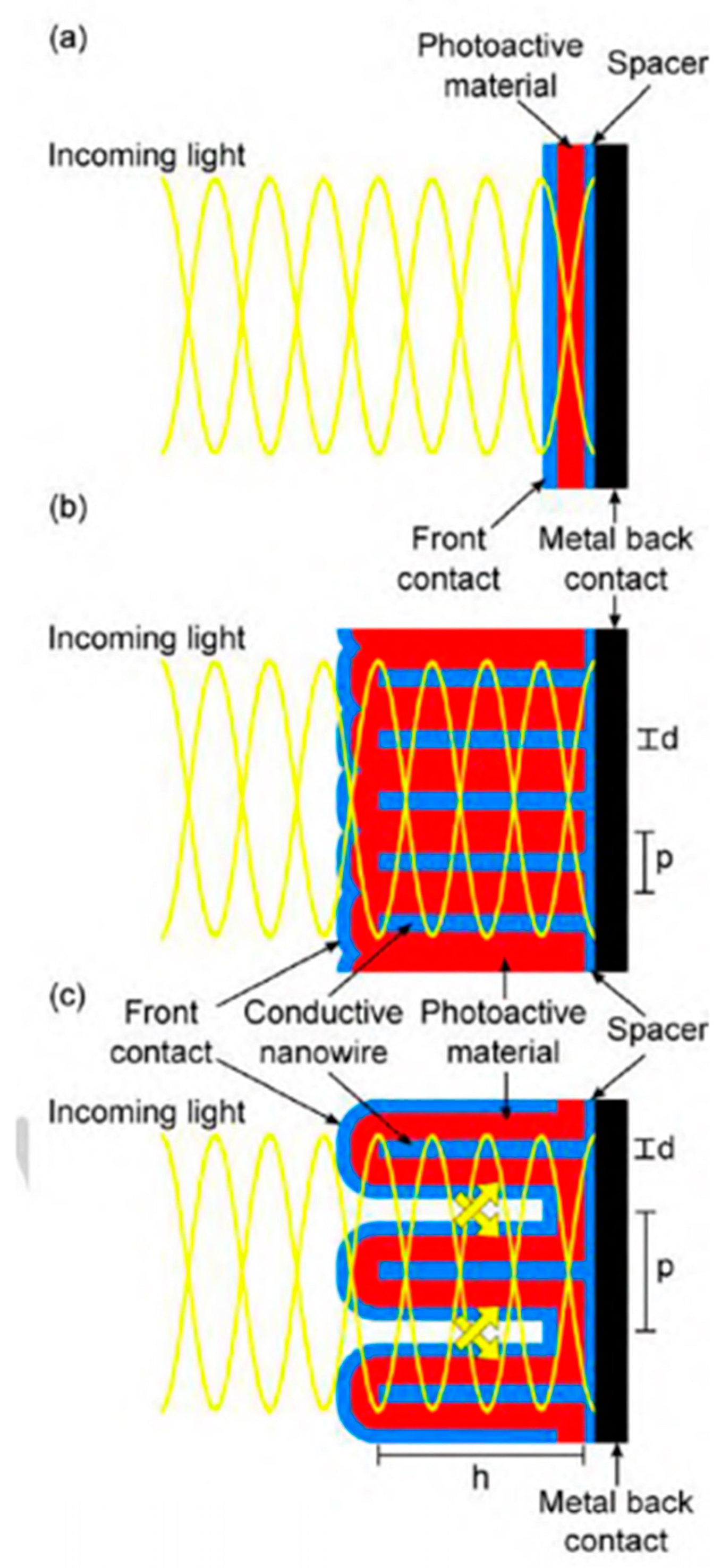
2.4. Not Affected by the Standing Wave Effect

In traditional photolithography techniques, especially during the transfer of complex or high-resolution patterns, the standing wave effect often becomes an unavoidable problem [80,81,82,83,84,85]. The standing wave effect originates from the interference phenomenon of the light source [86,87,88,89]. During the photolithography process, when the exposure light source forms a standing wave on the surface of the photoresist, it will cause uneven distribution of exposure intensity at different positions [90,91]. This non-uniformity directly affects the exposure of photoresist, leading to distortion or incomplete transfer of patterns, especially when dealing with complex graphics [92]. The impact of standing wave effect is more significant, and in severe cases, it may cause severe distortion of patterns, thereby affecting the quality and yield of the final product [93].
Unlike this, nanoimprint lithography technology directly transfers mold patterns to the substrate surface through physical contact, without needing pattern transfer through light source radiation [94], as shown in Figure 1. Since the exposure method of NIL technology is achieved through direct contact between the mold and the substrate, it does not rely on the propagation and interference of light, thus avoiding the interference of standing wave effect on the pattern transfer process. This direct transfer mechanism enables nanoimprint lithography to ensure the precise replication of complex patterns without being affected by non-uniformity that may occur during light wave propagation, greatly improving the stability and repeatability of the process.
In addition, the advantage of nanoimprint lithography technology has important practical significance in improving the accuracy and consistency of pattern transfer. The existence of the standing wave effect in traditional lithography not only increases the complexity and difficulty of the process but also requires fine process control and equipment optimization to minimize its negative effects. The characteristic of NIL being free from standing wave effects gives it a natural advantage in handling high-density and complex graphics, enabling it to maintain higher graphic resolution and transfer quality.
This characteristic makes nanoimprint lithography technology particularly advantageous for processing extremely fine and complex nano-structures, especially in fields such as semiconductor manufacturing [95], photonic devices [96], microfluidic chips [97,98,99,100], etc. Due to not needing to worry about standing wave effects, NIL can maintain high pattern consistency and product quality at lower costs and simpler process conditions. This has demonstrated significant technological advantages and stronger industrialization and commercialization potential for nanoimprint lithography technology in large-scale production, especially in application fields that require extremely high process requirements.

3. Challenges of Nanoimprint Lithography Technology

3.1. Thin Film Characteristic Issues

In the process of NIL, the elasticity and hardness of the thin film are key factors determining the quality of the imprint. Due to the dependence of nanoimprint lithography technology on physical contact and imprint transfer between the mold and the film, the mechanical properties of the film directly affect the accuracy and consistency of pattern transfer. The selection of thin film materials has a crucial impact on the quality of the final product during this process.
Common nanoimprint lithography thin film materials, such as polydimethylsiloxane (PDMS), are widely used in this technology [101,102,103,104,105] due to their excellent elasticity and low glass transition temperature. PDMS material can achieve high-quality pattern transfer under low pressure conditions and is suitable for imprinting on flexible substrates. However, although the elasticity of PDMS helps improve the contact between the mold and the substrate, it is prone to deformation during the embossing process, especially when processing high-precision patterns, where local expansion or contraction may occur. This deformation will lead to instability and fluctuations in line width, thereby affecting the accuracy of the pattern and ultimately impacting the yield and consistency of the entire manufacturing process, as shown in Figure 2.
On the other hand, materials such as polyethylene terephthalate (PET) [106,107,108] and polyvinyl alcohol (PVA) [109,110] have a high degree of hardness and strong mechanical stability, which enables them to effectively avoid line width fluctuations caused by deformation during the embossing process. These materials with higher degrees of hardness can maintain structural stability under greater pressure, thereby providing higher pattern accuracy, especially when dealing with fine structures. However, the increase in hardness also brings potential problems. When significant pressure is applied during the embossing process, materials with a high degree of hardness may cause damage or scratches to the target substrate, especially on hard substrates or brittle materials. This sort of damage not only affects the structural integrity of the substrate but may also lead to further damage to equipment and production lines, increasing manufacturing costs, as shown in Figure 3.
Therefore, when selecting suitable thin film materials, it is necessary to comprehensively consider the elasticity, hardness, and compatibility with the substrate of the material. The ideal thin film material should have moderate elasticity and hardness to ensure pattern accuracy while avoiding damage to the substrate. In practical applications, researchers and engineers typically optimize the performance of thin film materials by adjusting their thickness, hardness, and coating process. For example, composite material design or coating technology can enhance the film surface’s hardness while maintaining lower elasticity at the contact interface between the substrate and the film, thereby achieving a more ideal embossing effect.
The elasticity and hardness of thin films directly affect the quality and production efficiency of pattern transfer in nanoimprint lithography [111]. With the continuous advancement of materials science, new thin film materials may be developed to maintain sufficient elasticity while avoiding potential damage to high hardness materials, thereby optimizing the overall performance of nanoimprint lithography technology. In recent years, by introducing silicon carbide (SiC) hard coatings, PDMS, and other composite materials, as shown in Figure 4, deformation can be reduced while maintaining elasticity.

3.2. Application Limitations in Precision Chip Manufacturing

Although NIL technology has shown many advantages in the field of micro- and nano-manufacturing, especially given its high resolution, low cost, and simplified process flow, its application in precision chip manufacturing still faces certain technical limitations. Especially in the precision chip manufacturing process that requires extremely high manufacturing accuracy, the maturity and controllability of nanoimprint lithography technology still cannot fully compete with traditional lithography technology.
Precision chips, such as high-end semiconductor chips, quantum computing chips, and photonic integrated chips, typically require extremely high pattern accuracy and strict size control, especially in processes below the nanoscale. Traditional photolithography techniques, especially EUV lithography, with short wavelength and high-precision exposure systems, can achieve high-quality pattern transfer at very small scales and effectively handle complex multi-level structures. In contrast, although nanoimprint lithography can provide sub nanometer resolution, it is often limited by various factors such as mold accuracy, imprinting force, and film characteristics in practical applications, which may lead to errors in pattern transfer in chip manufacturing with extreme precision requirements [112,113,114,115].
High precision molds are the key to ensuring high-quality transfer patterns, but even the most precise molds may experience wear, aging, or small deformations during long-term use or large-scale production, contributing to a direct impact on the accuracy of the patterns. Compared to traditional photolithography techniques, masks and exposure systems can be corrected for errors through high-precision adjustment and multiple calibrations, making their accuracy more stable in long-term large-scale production.
In the process of chip manufacturing, the flatness, cleanliness, and material selection of the substrate surface significantly impact the accuracy of pattern transfer. Especially in the transfer of large-area and high-density patterns, there may be slight changes or unevenness in the substrate, which can lead to distortion or misalignment of the pattern. Traditional lithography techniques, especially EUV lithography, can effectively compensate for these effects and maintain high manufacturing accuracy through precise optical systems.
Although the nondevelopment characteristics, low cost, and high resolution of nanoimprint lithography give it significant advantages in certain application scenarios, there are still uncertainties in the production process regarding precision chip manufacturing that requires high precision and stability. For example, during the embossing process, there may be quality fluctuations in pattern transfer due to external environmental changes (such as temperature fluctuations and humidity changes) or equipment instability, which may affect the yield and performance of the final product in the manufacturing of high-end chips. With the advancement of technology and the deepening of research, nanoimprint lithography is expected to overcome existing limitations and gradually catch up with traditional lithography technology. However, in the short term, its application in precision chip manufacturing may still be limited to a certain extent.

4. Application of Nanoimprint Lithography in Different Industries

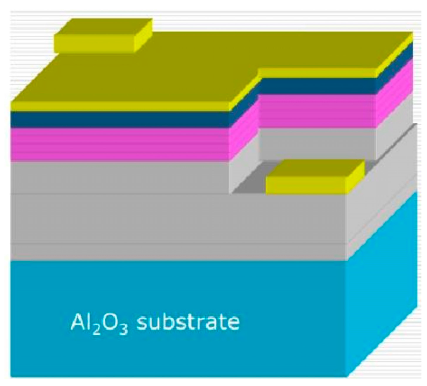
4.1. Patterned Sapphire Substrates

Patterned sapphire substrates (PSSs) are a key component of the current LED (Light-Emitting Diode) industry and play an important role in improving the light extraction efficiency and performance stability of LED devices [116,117,118,119,120]. PSSs mainly change the propagation path of light by forming periodic micro- and nano-patterns on the surface of sapphire substrates (as shown in Figure 5), improving the scattering and reflection effects of light. This reduces the total internal reflection of light at the substrate interface and increases the light output rate [121]. At the same time, this periodic structure can effectively reduce the dislocation density of LED chips and improve the crystal quality of epitaxial layers, thereby enhancing the optoelectronic performance of the device, as shown in Figure 6 [122].
Compared to traditional photolithography techniques, NIL has demonstrated significant technological advantages in the PSS manufacturing process [123]. Due to the relatively low requirement for lithography accuracy in PSSs, NIL’s high resolution, low cost, and large-area patterning capability make it an ideal technology choice in this field. Through NIL technology, highly uniform micro- and nano-structures can be quickly formed on large-area sapphire substrates, improving production efficiency and reducing manufacturing costs [124].
In recent years, with the continuous development of the LED industry, the demand for optical and structural optimization of traditional PSSs has gradually increased, and patterned sapphire composite substrates (PSCs) have emerged, as shown in Figure 7. PSCs introduce optical functional materials such as silicon dioxide (SiO2) as the main component of the patterned structure based on traditional PSSs, while sapphire remains the substrate material [125]. This composite structure can further optimize the optical performance of LED and achieve better light scattering and reflection control while reducing lattice mismatch stress during epitaxial growth and improving the quality of epitaxial layers.
Nanoimprint lithography also plays an important role in PSC manufacturing. Compared to traditional dry etching processes, NIL can directly transfer high-precision SiO2 patterned structures onto sapphire substrates, which not only simplifies the process but also reduces production costs and equipment complexity. In addition, the high uniformity and high-resolution characteristics of NIL enable it to achieve uniform and controllable SiO2 patterns on large-area substrates, ensuring consistency and reliability of LED chips in mass production, as shown in Figure 8.
In summary, nanoimprint lithography technology has demonstrated significant advantages in PSS and PSC manufacturing, not only meeting the LED industry’s demand for large-scale, low-cost manufacturing but also further optimizing the optical and structural characteristics of LED chips through refined pattern design. With the continuous development of NIL technology, its application potential in the field of patterned sapphire substrates and composite substrates will be further expanded and will lead the development of the LED industry towards higher efficiency and lower cost.

4.2. LED Chip Manufacturing

The manufacturing of LED chips involves a series of precision processes, among which the accuracy of photolithography technology significantly impacts the final performance of the device. Compared with traditional semiconductor chip manufacturing, LED chips have relatively lower requirements for lithography accuracy, usually meeting production needs in the micrometer or even sub-micrometer range. The specific structure is shown in Figure 9. The LED epitaxial structure typically consists of multiple layers of semiconductor materials, grown on a substrate. The fundamental layers include a sapphire or silicon carbide substrate, a buffer layer to accommodate lattice mismatches, and multiple epitaxial layers of gallium nitride (GaN). These layers are structured to form a p-n junction, which is crucial for light emission. The n-type layer is doped with silicon, while the p-type layer is doped with magnesium. This arrangement facilitates efficient electron–hole recombination, producing light when an electric current passes through the LED. However, due to the trend of improving the light efficiency, optimizing the structure, and miniaturizing LED chips [126,127,128], higher requirements have been put forward for the accuracy, uniformity, and cost control of photolithography processes. Therefore, finding a photolithography technology that can improve production efficiency and reduce costs while ensuring high precision has become an important research direction in the LED industry [129].
NIL has demonstrated significant advantages in LED chip manufacturing. Compared to traditional photolithography processes such as photolithography and electron beam lithography, NIL does not rely on expensive optical systems or electron beam equipment but directly transfers pre-defined nanometer or micrometer level patterns through physical imprinting. This direct imprinting method not only simplifies the photolithography process but also enables highly uniform pattern replication on large-area substrates, significantly reducing production costs and increasing production capacity [130].
In the manufacturing process of LED chips, NIL can be used for multiple key steps, such as forming electrode patterns, etching micro- and nano-structures to improve Light Extraction Efficiency (LEE), and manufacturing photonic crystal structures. Among them, nanoimprint lithography is particularly suitable for constructing periodic photonic crystal structures or subwavelength structures on the surface of LED chips to enhance light scattering and extraction and improve the light output rate of LED chips. In addition, NIL can provide a high-precision and low-cost alternative solution in the metal electrode patterning process, optimize current distribution and reduce light loss, thereby further improving the overall performance of LED devices.
The application of nanoimprint lithography in LED chip manufacturing is also reflected in its high efficiency and mass production capability. Compared to traditional photolithography processes, NIL can achieve large-area, multi-chip patterning in a single imprint process, greatly improving production efficiency. Meanwhile, as the NIL process can be applied to flexible and curved substrates, it provides more possibilities for the development of future flexible LEDs, micro LEDs, and new optoelectronic devices.
Although NIL has many advantages in LED chip manufacturing, there are still some technical challenges that need to be overcome. For example, mold lifespan, pattern transfer accuracy, and adaptability to different substrate materials remain key factors affecting its large-scale application. Therefore, current research mainly focuses on improving the durability of NIL molds, optimizing anti adhesion layers to reduce pollution, and combining other advanced processes such as self-assembled nanosphere lithography or hybrid lithography to further enhance their process applicability and yield.
Nanoimprint lithography technology, with its advantages of high precision, high efficiency, and low cost, has become an important technical means for LED chip manufacturing and plays a key role in improving the optical performance of LED chips, reducing production costs, and promoting the development of new LED technologies. With the continuous optimization of NIL technology and further maturity of equipment, its application in LED manufacturing will be further expanded, and it is expected to promote the development of the LED industry towards higher efficiency and intelligence.

4.3. Photovoltaic Cell Manufacturing

As an important renewable energy technology, photoelectric conversion efficiency during the manufacturing process of photovoltaic cells directly determines the economy and application scope of solar power generation. In the manufacturing process of photovoltaic cells, the design of surface structure is crucial, especially the light scattering characteristics of the cell surface, which have a direct impact on the absorption of light and the collection efficiency of current. The traditional surface structure of photovoltaic cells is usually formed into a textured surface through chemical corrosion methods. This surface treatment process can effectively enhance light scattering and improve the light absorption capacity of photovoltaic cells. However, traditional chemical corrosion processes have some shortcomings, mainly manifested in the fluctuation and uncontrollability of surface texture structure, which directly affects the stability and consistency of photovoltaic cells, thereby affecting the performance and long-term reliability of the cells [131].
In traditional corrosion methods, the microstructure of the battery surface is usually formed by corrosion with acidic or alkaline solutions. Although this method can improve the scattering performance of the battery to a certain extent, due to the randomness and complexity of the corrosion process, the resulting suede morphology often has significant fluctuations. This volatility not only leads to non-uniformity of the surface structure but may also cause differences in current collection efficiency in different regions of the photovoltaic cell, thereby affecting the output power and stability of the entire cell. Therefore, how to manufacture precise and stable micro- and nano-structures on the surface of photovoltaic cells has become the key to improving the performance of photovoltaic cells [132].
In order to overcome the limitations of traditional corrosion processes, researchers have proposed the method of photolithography etching to form stable micro- and nano-structures on the surface of photovoltaic cells, as shown in Figure 10. Compared with traditional corrosion processes, photolithography technology can accurately control the shape and size of patterns on the surface of batteries, ensuring the uniformity and repeatability of the battery surface structure. However, although photolithography technology can provide higher accuracy and stability, traditional photolithography processes (especially ultraviolet lithography and electron beam lithography) often require expensive masks, complex development processes, and high equipment investment, which undoubtedly increases the cost of photovoltaic cell manufacturing and limits its large-scale application [133].
At this point, NIL has become an ideal alternative due to its unique low-cost advantage. Nanoimprint lithography transfers patterns to the surface of batteries directly using mold imprinting [134,135,136,137]. Compared to traditional lithography techniques, NIL does not require expensive masking and development steps. Its core advantage lies in the fact that high-precision and high-quality surface micro- and nano-structure manufacturing can be achieved through embossing technology, while greatly reducing process costs. In addition, NIL technology can operate at lower temperatures and pressures, avoiding the high temperature annealing and pollution problems that may occur in traditional photolithography techniques, further improving the manufacturing efficiency of photovoltaic cells.
After applying NIL technology in photovoltaic cell manufacturing, stable and uniform micro- and nano-structures can be formed on the surface of the cell, thereby improving the scattering effect of light and enhancing the absorption capacity of photovoltaic cells for light. Especially for polycrystalline silicon solar cells, NIL technology can manufacture efficient surface photonic crystal structures at a lower cost. This structure not only effectively enhances light scattering but also improves the photoelectric conversion efficiency and long-term stability of the cell to a certain extent [138].
In summary, nanoimprint lithography technology provides a low-cost, efficient, and controllable solution for the manufacturing of photovoltaic cells. Through NIL technology, the microstructure of the surface of photovoltaic cells can be precisely controlled, overcoming the problems of unstable and fluctuating surface structure in traditional corrosion processes, thereby effectively improving the photoelectric conversion efficiency and reliability of photovoltaic cells. With the continuous maturity and industrialization of NIL technology, its widespread application in photovoltaic cell manufacturing will further promote the development of the solar energy industry, reduce the production cost of photovoltaic cells, and improve their market competitiveness.

4.4. Applications in Other Fields

NIL technology plays a crucial role in many cutting-edge applications, especially in the field of metasurfaces. As a new type of two-dimensional material structure, metasurfaces have unique optical properties that enable precise control of light propagation and reflection at the nanoscale. Therefore, they have shown great potential in applications such as metal lenses, optical filters, anti-reflective coatings, and augmented reality. For example, manufacturing metal lenses requires precise nano-structures to achieve specific optical properties [109,139], and NIL technology can maintain high precision in large-scale production. At the same time, NIL has demonstrated outstanding advantages in manufacturing optical filters and anti-reflective coatings, achieving higher optical transmission efficiency and better surface optical performance, thereby promoting the performance improvement of optoelectronic devices [140,141,142]. With the rise in augmented reality (AR) technology, NIL technology is increasingly important in manufacturing metasurfaces suitable for AR display devices. It can precisely control the surface morphology at the micrometer to nanometer scale, greatly promoting the application of metasurfaces in this emerging field. NIL technology has demonstrated irreplaceable advantages in the manufacturing of metasurfaces and is expected to play an important role in multiple high-tech fields in the future.

5. Cost Analysis of Nanoimprint Lithography

NIL has demonstrated superior performance in multiple fields, especially in cost control. Compared to traditional photolithography techniques, NIL’s cost advantages mainly lie in selecting photoresist, simplifying process flow, and reducing equipment investment.
The cost of photoresist used in nanoimprint lithography technology is relatively low. The traditional photolithography process usually uses positive photoresist, which has a high preparation cost and requires multiple steps such as exposure and development during the photolithography process. In the NIL process, negative photoresist is usually used, which is generally cheaper in the market. In addition, the unique feature of NIL technology is that it does not require a development process, which not only simplifies the process flow, but also further reduces material consumption and lowers waste disposal costs. The development process in traditional photolithography technology requires a large amount of developer solutions and chemicals, and there are problems with waste liquid treatment and environmental pollution. However, NIL reduces these complex steps by directly imprinting patterns.
The NIL process can significantly reduce equipment investment costs due to its simplified process and fewer steps. NIL technology directly transfers patterns through mold imprinting, greatly reducing reliance on high-precision optical equipment. At the same time, the cost of mold production and maintenance is much lower than that of traditional photolithography mask production.
Nanoimprint lithography technology effectively reduces the overall production cost by reducing the cost of photoresist, simplifying the process flow, and reducing equipment investment, making it a low-cost and efficient production technology with wide application potential in multiple fields. This cost advantage enables NIL to achieve large-scale production, especially in optoelectronics LEDs. In industries such as photovoltaics, there is significant potential for application.

6. The Industrialization Prospects of Nanoimprint Lithography

With the continuous advancement and optimization of NIL technology, its industrialization prospects are gradually becoming clear. The low cost, high efficiency, and high precision characteristics of NIL technology have shown great potential for application in multiple industries, especially in fields such as LED, photovoltaics, and photonic crystal structures (PSSs), where its advantages are even more prominent. In the future, with further technological development, NIL is expected to become one of the mainstream manufacturing processes in these fields.
In the field of LED manufacturing, NIL technology can effectively improve light extraction efficiency and current distribution by precisely etching micro- and nano-structures on silicon substrates, thereby enhancing the light efficiency and lifespan of LEDs. Compared to traditional photolithography technology, NIL can achieve high-precision and low-cost pattern transfer in the production process, making it particularly suitable for large-scale production and meeting the market’s demand for efficient and low-cost LED chips. As the application of NIL technology in LED manufacturing gradually matures, it is expected to drive the transformation of the entire LED industry’s production mode and bring significant cost savings and performance improvements.
In the photovoltaic industry, by constructing micro- and nano-structures on the surface of the battery, NIL can significantly increase light scattering and absorption, improving the overall performance of photovoltaic cells. In addition, NIL’s adaptability to flexible substrates makes flexible photovoltaic cells and integrated photovoltaic systems an important direction for future development. With the continuous advancement of material innovation and process optimization, NIL technology is expected to be widely applied in the photovoltaic industry, promoting the development of renewable energy technology.
The manufacturing of photonic crystal structures (PSSs) is also an important application area of NIL technology. By manufacturing periodic micro- and nano-structures on the surface of photonic devices, NIL can effectively enhance light scattering, refraction, and modulation, thereby improving the performance of photonic devices. In the fields of optical communication, optical detection, and lasers, NIL technology can significantly improve device performance and promote the development of related industries through high-precision patterning.
In the future, material innovation and process optimization will be key factors driving the industrialization process of NIL. At present, the challenges faced by NIL technology mainly include the durability of mold materials, control of mold production costs, and yield issues in the production process. With the continuous advancement of nanomaterials, super-resolution photoresist, and mold materials, NIL’s production capacity, accuracy, and reliability will be further improved. At the same time, the construction of integrated and automated production lines will also promote the large-scale application of NIL technology, especially in the fields of high-performance electronic devices, flexible electronics, sensors, and biomedical devices. Although NIL has been commercialized in the fields of LED and photonic devices (such as EV Group’s NIL equipment), it still faces competition from the traditional photolithography ecosystem in semiconductor manufacturing and needs to break through industry standard barriers.
To fully unlock the potential of NIL in high-precision and emerging fields, several critical technological advancements are imperative. First, developing ultra-durable mold materials with atomic-level smoothness and anti-adhesion properties is essential to extend mold lifespan and enable sub-5 nm resolution imprinting. Second, hybrid lithography approaches combining NIL with directed self-assembly (DSA) or multi-photon lithography could bridge the gap between high-throughput patterning and nanoscale precision, particularly for 3D nano-structures. Third, intelligent process control systems integrating real-time monitoring (e.g., in situ optical metrology) and machine learning algorithms are needed to address alignment errors and defect propagation in roll-to-roll manufacturing. Additionally, integrating NIL with emerging flexible substrates (e.g., 2D materials) and bio-compatible resists will open new frontiers in wearable electronics and nanomedicine. Addressing these challenges will position NIL as a cornerstone technology for next-generation semiconductor nodes, quantum photonics, and sustainable nanomanufacturing.
Nanoimprint lithography technology has unique advantages of low cost, high efficiency, and high precision. With the continuous optimization of technology and innovation of materials, NIL has broad prospects for industrialization in multiple industries. With the further improvement of processes and equipment, NIL is expected to become one of the important technologies in the future manufacturing industry, promoting the development of related fields and replacing traditional processes in large-scale production, forming a new industrial pattern.

7. Conclusions

This article discussed the application of NIL technology in modern manufacturing in detail. Firstly, the advantages of NIL in photovoltaic cell manufacturing were introduced, emphasizing its ability to effectively reduce costs while ensuring high precision, especially in large-scale production, demonstrating enormous potential for application. By replacing traditional photolithography techniques, NIL not only reduces the need for expensive photoresist and equipment but also optimizes the manufacturing of micro and nano structures on the surface of photovoltaic cells, improves photoelectric conversion efficiency, and promotes technological progress in the photovoltaic industry. This article analyzes the cost advantages of NIL and points out that this technology has significant cost saving potential compared to traditional photolithography processes in terms of photoresist, development process, and equipment investment. Especially with the use of negative photoresist and the omission of development processes, NIL has become an ideal choice for low-cost large-scale production, which is of great significance for promoting the rapid development of industries such as electronics, photonics, and LEDs. The core competitiveness of NIL lies in its low cost and high efficiency in low to medium precision scenarios, and in the future, it needs to promote industrialization through process standardization and cross industry collaboration. This article anticipates the industrialization prospects of nanoimprint lithography technology. The low cost, high efficiency, and high precision of NIL technology make it widely applicable in fields such as LEDs, photovoltaics, and photonic crystal structures (PSSs). Although currently facing technological challenges such as mold materials and process stability, with the continuous maturity of related technologies, NIL’s industrialization process will usher in breakthroughs, promoting the development of various fields towards high efficiency, low cost, and sustainability.

Author Contributions

Conceptualization, Y.C. and Z.Y.; methodology, Y.C.; validation, Z.Y.; formal analysis, D.M.; investigation, H.L.; resources, Z.Y.; data curation, Y.C.; writing—original draft preparation, Y.C.; writing—review and editing, Y.C. and Z.Y.; visualization, G.C.; supervision, J.Z.; project administration, Z.Y. All authors have read and agreed to the published version of the manuscript.

Funding

This research was supported by the 2024 Jilin Provincial Department of Education Science Research Project “Preparation and Application of New Self heating Composite Nanoimprint Film” (project no. JJKH20241130KJ).

Institutional Review Board Statement

Not applicable.

Informed Consent Statement

Not applicable.

Data Availability Statement

The data that support the findings of this study are available from the corresponding author upon reasonable request.

Conflicts of Interest

The authors declare that they have no known competing financial interests or personal relationships that could have appeared to influence the work reported in this paper.

Abbreviations

The following abbreviations are used in this manuscript:
NILNanoimprint Lithography
PSSspatterned sapphire substrates
EUVextreme ultraviolet
DUVdeep ultraviolet
PSCpatterned sapphire composite substrate
LEDLight-Emitting Diode

References

  1. Singh, N.H.; Moirangthem, R.S.; Meitei, S.R.; Singh, N.M. Fabrication and Characterization of Zinc oxide nanorods-Modified Electrodes using Nanoimprint Lithography for electrochemical sensing of heavy metal ions. Thin Solid Film. 2024, 807, 140550. [Google Scholar] [CrossRef]
  2. Zhu, K.; Wen, C.; Aljarb, A.A.; Xue, F.; Xu, X.; Tung, V.; Zhang, X.; Alshareef, H.N.; Lanza, M. The development of integrated circuits based on two-dimensional materials. Nat. Electron. 2021, 4, 775–785. [Google Scholar] [CrossRef]
  3. Ha, D.; Fang, Z.; Zhitenev, N.B. Paper in electronic and optoelectronic devices. Adv. Electron. Mater. 2018, 4, 1700593. [Google Scholar] [CrossRef]
  4. Cai, Y.; Qin, A.; Tang, B.Z. Siloles in optoelectronic devices. J. Mater. Chem. C 2017, 5, 7375–7389. [Google Scholar] [CrossRef]
  5. Bodnariuk, M.; Melentiev, R. Bibliometric analysis of micro-nano manufacturing technologies. Nanotechnol. Precis. Eng. 2019, 2, 61–70. [Google Scholar] [CrossRef]
  6. Fidan, I.; Ali, M.A.; Naikwadi, V.; Gudavasov, S.; Mahmudov, M.; Mohammadizadeh, M.; Zhang, Z.; Sharma, A. Nano-Level Additive Manufacturing: Condensed Review of Processes, Materials, and Industrial Applications. Technologies 2024, 12, 117. [Google Scholar] [CrossRef]
  7. Huang, X.; Qi, Y.; Bu, T.; Li, X.; Liu, G.; Zeng, J.; Fan, B.; Zhang, C. Overview of advanced micro-nano manufacturing technologies for triboelectric nanogenerators. Nanoenergy Adv. 2022, 2, 316–343. [Google Scholar] [CrossRef]
  8. Wu, Q.; Li, Y.; Zhao, Y. The evolution of photolithography technology, process standards, and future outlook. In Proceedings of the 2020 IEEE 15th International Conference on Solid-State & Integrated Circuit Technology (ICSICT), Kunming, China, 3–6 November 2020. [Google Scholar]
  9. Ji, T.; Jin, S.; Zhang, H.; Chen, S.; Sun, X. Full color quantum dot light-emitting diodes patterned by photolithography technology. J. Soc. Inf. Disp. 2018, 26, 121–127. [Google Scholar] [CrossRef]
  10. Chen, Z.; Li, Y.; Man, Z.; Tang, A. Research progress of quantum dot photolithography patterning and direct photolithography application. Nano Res. 2024, 17, 10386–10411. [Google Scholar] [CrossRef]
  11. Kazazis, D.; Santaclara, J.G.; van Schoot, J.; Mochi, I.; Ekinci, Y. Extreme ultraviolet lithography. Nat. Rev. Methods Primers 2024, 4, 84. [Google Scholar] [CrossRef]
  12. Fomenkov, I.; Brandt, D.; Ershov, A.; Schafgans, A.; Tao, Y.; Vaschenko, G.; Rokitski, S.; Kats, M.; Vargas, M.; Purvis, M.; et al. Light sources for high-volume manufacturing EUV lithography: Technology, performance, and power scaling. Adv. Opt. Technol. 2017, 6, 173–186. [Google Scholar] [CrossRef]
  13. Miyazaki, J.; Yen, A. EUV lithography technology for high-volume production of semiconductor devices. J. Photopolym. Sci. Technol. 2019, 32, 195–201. [Google Scholar] [CrossRef]
  14. van de Kerkhof, M.; Liu, F.; Meeuwissen, M.; Zhang, X.; Bayraktar, M.; de Kruif, R.; Davydova, N. High-power EUV lithography: Spectral purity and imaging performance. J. Micro/Nanolithogr. MEMS MOEMS 2020, 19, 033801. [Google Scholar] [CrossRef]
  15. Taguchi, A.; Nakayama, A.; Oketani, R.; Kawata, S.; Fujita, K. Multiphoton-excited deep-ultraviolet photolithography for 3D nanofabrication. ACS Appl. Nano Mater. 2020, 3, 11434–11441. [Google Scholar] [CrossRef]
  16. Rice, B.J. Extreme ultraviolet (EUV) lithography. In Nanolithography; Woodhead Publishing: Cambridge, UK, 2014; pp. 42–79. [Google Scholar]
  17. Mack, C.A. Reducing roughness in extreme ultraviolet lithography. J. Micro/Nanolithogr. MEMS MOEMS 2018, 17, 041006. [Google Scholar] [CrossRef]
  18. Itani, T.; Kozawa, T. Resist materials and processes for extreme ultraviolet lithography. Jpn. J. Appl. Phys. 2012, 52, 010002. [Google Scholar] [CrossRef]
  19. Ober, C.K.; Käfer, F.; Yuan, C. Recent developments in photoresists for extreme-ultraviolet lithography. Polymer 2023, 280, 126020. [Google Scholar] [CrossRef]
  20. Wang, X.; Tao, P.; Wang, Q.; Zhao, R.; Liu, T.; Hu, Y.; Hu, Z.; Wang, Y.; Wang, J.; Tang, Y.; et al. Trends in photoresist materials for extreme ultraviolet lithography: A review. Mater. Today 2023, 67, 299–319. [Google Scholar] [CrossRef]
  21. Peng, Z.; Zhang, Y.; Choi, C.L.R.; Zhang, P.; Wu, T.; Chan, Y.K. Continuous roller nanoimprinting: Next generation lithography. Nanoscale 2023, 15, 11403–11421. [Google Scholar] [CrossRef]
  22. Cui, S.; Sun, K.; Liao, Z.; Zhou, Q.; Jin, L.; Jin, C.; Hu, J.; Wen, K.-S.; Liu, S.; Zhou, S. Flexible nanoimprint lithography enables high-throughput manufacturing of bioinspired microstructures on warped substrates for efficient III-nitride optoelectronic devices. Sci. Bull. 2024, 69, 2080–2088. [Google Scholar] [CrossRef]
  23. Takeishi, H.; Sreenivasan, S.V. Nanoimprint system development and status for high volume semiconductor manufacturing. In Proceedings of the Alternative Lithographic Technologies VII, SPIE Advanced Lithography, San Jose, CA, USA, 22–26 February 2015; Volume 9423, pp. 49–57. [Google Scholar]
  24. Chou, S.Y.; Krauss, P.R.; Zhang, W.; Guo, L.; Zhuang, L. Sub-10 nm imprint lithography and applications. J. Vac. Sci. Technol. B Microelectron. Nanometer Struct. Process. Meas. Phenom. 1997, 15, 2897–2904. [Google Scholar] [CrossRef]
  25. Shao, J.; Chen, X.; Li, X.; Tian, H.; Wang, C.; Lu, B. Nanoimprint lithography for the manufacturing of flexible electronics. Sci. China Technol. Sci. 2019, 62, 175–198. [Google Scholar] [CrossRef]
  26. Kooy, N.; Mohamed, K.; Pin, L.T.; Guan, O.S. A review of roll-to-roll nanoimprint lithography. Nanoscale Res. Lett. 2014, 9, 1–13. [Google Scholar] [CrossRef] [PubMed]
  27. Modaresialam, M.; Chehadi, Z.; Bottein, T.; Abbarchi, M.; Grosso, D. Nanoimprint Lithography Processing of Inorganic-Based Materials. Chem. Mater. 2021, 33, 5464–5482. [Google Scholar] [CrossRef]
  28. Shao, J.; Chen, X.; Li, X.; Tian, H.; Wang, C.; Lu, B. A versatile pattern inversion process based on thermal and soft UV nanoimprint lithography techniques. Microelectron. Eng. 2010, 87, 899–903. [Google Scholar]
  29. Park, T.W.; Kang, Y.L.; Kang, E.B.; Kim, S.; Kim, Y.N.; Park, W.I. Formation of Multiscale Pattern Structures by Combined Patterning of Nanotransfer Printing and Laser Micromachining. Nanomaterials 2023, 13, 2327. [Google Scholar] [CrossRef] [PubMed]
  30. Cheng, X. Nanostructures: Fabrication and applications. In Nanolithography; Woodhead Publishing: Cambridge, UK, 2014; pp. 348–375. [Google Scholar]
  31. Yao, X.; Peng, R.; Ding, J. Cell–material interactions revealed via material techniques of surface patterning. Adv. Mater. 2013, 25, 5257–5286. [Google Scholar] [CrossRef]
  32. Luo, X. Fabrication techniques. In Engineering Optics 2.0: A Revolution in Optical Theories, Materials, Devices and Systems; Springer: Singapore, 2019; pp. 179–242. [Google Scholar]
  33. Cui, Z. Nanoimprint Lithography. In Nanofabrication: Principles, Capabilities and Limits; Springer International Publishing: Cham, Switzerland, 2024; pp. 201–255. [Google Scholar]
  34. Sharma, E.; Rathi, R.; Misharwal, J.; Sinhmar, B.; Kumari, S.; Dalal, J.; Kumar, A. Evolution in lithography techniques: Microlithography to nanolithography. Nanomaterials 2022, 12, 2754. [Google Scholar] [CrossRef]
  35. Cojocaru, C.V.; Cicoira, F.; Rosei, F. Alternative Nanofabrication Approaches for non-CMOS Applications. In Nanofabrication Fundamentals and Applications; World Scientific Publishing Co.: Singapore, 2008; pp. 499–542. [Google Scholar]
  36. Sun, H.; Li, L.; Gu, L.; Wang, J.; Zhang, L.; Gu, Y.; Bao, X. Nanoimprint Lithography for Solar Cell Applications. J. Nanoelectron. Optoelectron. 2024, 19, 1075–1097. [Google Scholar] [CrossRef]
  37. Ma, R.; Zhang, X.; Sutherland, D.; Bochenkov, V.; Deng, S. Nanofabrication of nanostructure lattices: From high-quality large patterns to precise hybrid units. Int. J. Extrem. Manuf. 2024, 6, 062004. [Google Scholar] [CrossRef]
  38. Boltasseva, A.; Shalaev, V.M. Fabrication of optical negative-index metamaterials: Recent advances and outlook. Metamaterials 2008, 2, 1–17. [Google Scholar] [CrossRef]
  39. Dumond, J.J.; Low, H.Y. Recent developments and design challenges in continuous roller micro-and nanoimprinting. J. Vac. Sci. Technol. B 2012, 30, 010801. [Google Scholar] [CrossRef]
  40. Wisser, F.M.; Schumm, B.; Mondin, G.; Grothe, J.; Kaskel, S. Precursor strategies for metallic nano-and micropatterns using soft lithography. J. Mater. Chem. C 2015, 3, 2717–2731. [Google Scholar] [CrossRef]
  41. Ooi, Y.K.; Zhang, J. Light extraction efficiency analysis of flip-chip ultraviolet light-emitting diodes with patterned sapphire substrate. IEEE Photonics J. 2018, 10, 1–13. [Google Scholar] [CrossRef]
  42. Hsiang, E.L.; He, Z.; Huang, Y.; Gou, F.; Lan, Y.F.; Wu, S.T. Improving the power efficiency of micro-LED displays with optimized LED chip sizes. Crystals 2020, 10, 494. [Google Scholar] [CrossRef]
  43. Nayak, P.K.; Mahesh, S.; Snaith, H.J.; Cahen, D. Photovoltaic solar cell technologies: Analysing the state of the art. Nat. Rev. Mater. 2019, 4, 269–285. [Google Scholar] [CrossRef]
  44. Guo, X.; Hu, J.; Zhuang, Z.; Deng, M.; Wu, F.; Li, X.; Liu, B.; Yuan, C.; Ge, H.; Li, F.; et al. Fabrication of wafer-scale nanopatterned sapphire substrate by hybrid nanoimprint lithography. J. Vac. Sci. Technol. B 2014, 32, 06FG06. [Google Scholar] [CrossRef]
  45. Zhou, S.; Zhao, X.; Du, P.; Zhang, Z.; Liu, X.; Liu, S.; Guo, L.J. Application of patterned sapphire substrate for III-nitride light-emitting diodes. Nanoscale 2022, 14, 4887–4907. [Google Scholar] [CrossRef]
  46. Chen, D.; Chen, Y.C.; Zeng, G.; Zhang, D.W.; Lu, H.L. Integration technology of micro-LED for next-generation display. Research 2023, 6, 0047. [Google Scholar] [CrossRef]
  47. Yu, B.; Li, Y.; Li, J.; Ding, X.; Li, Z. Challenges of high-yield manufacture in micro-light-emitting diodes displays: Chip fabrication, mass transfer, and detection. J. Phys. D Appl. Phys. 2024, 57, 463001. [Google Scholar] [CrossRef]
  48. Lee, T.Y.; Chen, L.Y.; Lo, Y.Y.; Swayamprabha, S.S.; Kumar, A.; Huang, Y.M.; Chen, S.C.; Zan, H.W.; Chen, F.C.; Horng, R.H.; et al. Technology and applications of micro-LEDs: Their characteristics, fabrication, advancement, and challenges. ACS Photonics 2022, 9, 2905–2930. [Google Scholar] [CrossRef]
  49. Gong, Y.; Gong, Z. Laser-Based Micro/Nano-Processing Techniques for Microscale LEDs and Full-Color Displays. Adv. Mater. Technol. 2023, 8, 2200949. [Google Scholar] [CrossRef]
  50. Wang, W.; Qi, L. Light management with patterned micro- and nanostructure arrays for photocatalysis, photovoltaics, and optoelectronic and optical devices. Adv. Funct. Mater. 2019, 29, 1807275. [Google Scholar] [CrossRef]
  51. Violas, A.F.; Oliveira, A.J.N.; Yakovleva, E.; Sieira, B.L.; Pinto, F.; Rocha, B.; Ribeiro, E.J.; Pinheiro, X.L.; Bondarchuk, O.; Capitão, J.; et al. One-Step Lithography Nanostructured Au Encapsulation for Light Management in Ultrathin ACIGS Solar Cells. Sol. RRL 2025, 9, 2400837. [Google Scholar] [CrossRef]
  52. Jeong, B.; Han, H.; Park, C. Micro- and nanopatterning of halide perovskites where crystal engineering for emerging photoelectronics meets integrated device array technology. Adv. Mater. 2020, 32, e2000597. [Google Scholar] [CrossRef] [PubMed]
  53. Pimpin, A.; Srituravanich, W. Review on micro-and nanolithography techniques and their applications. Eng. J. 2012, 16, 37–56. [Google Scholar] [CrossRef]
  54. Resnick, D.J.; Choi, J. A review of nanoimprint lithography for high-volume semiconductor device manufacturing. Adv. Opt. Technol. 2017, 6, 229–241. [Google Scholar] [CrossRef]
  55. Nagarjuna, R.; Thakur, A.; Balapure, A.; Saifullah, M.S.M.; Dutta, J.R.; Ganesan, R. Chemically amplified molecular resins for shrinkage-controlled direct nanoimprint lithography of functional oxides: An application towards dark-light dual-mode antibacterial surfaces. Mater. Adv. 2024, 5, 593–607. [Google Scholar] [CrossRef]
  56. Sun, Y.L.; Jevasuwan, W.; Fukata, N. Top-down fabrication of Ge nanowire arrays by nanoimprint lithography and hole gas accumulation in Ge/Si core-shell nanowires. Appl. Surf. Sci. 2024, 643, 158656. [Google Scholar] [CrossRef]
  57. Yao, Y.; Liu, H.; Wang, Y.; Li, Y.; Song, B.; Bratkovsk, A.; Wang, S.Y.; Wu, W. Nanoimprint lithography: An enabling technology for nanophotonics. Appl. Phys. A 2015, 121, 327–333. [Google Scholar] [CrossRef]
  58. Wu, D.; Nitul, S.R.; Luo, X. Nanoimprint lithography-the past, the present and the future. Curr. Nanosci. 2016, 12, 712–724. [Google Scholar] [CrossRef]
  59. Thielsch, R. Optical coatings for the DUV/VUV. In Optical Interference Coatings; Springer: Berlin/Heidelberg, Germany, 2003; pp. 257–279. [Google Scholar]
  60. Banine, V.; Moors, R. Plasma sources for EUV lithography exposure tools. J. Phys. D Appl. Phys. 2004, 37, 3207. [Google Scholar] [CrossRef]
  61. Alnakhli, Z.; Liu, Z.; AlQatari, F.; Cao, H.; Li, X. UV-assisted nanoimprint lithography: The impact of the loading effect in silicon on nanoscale patterns of metalens. Nanoscale Adv. 2024, 6, 2954–2967. [Google Scholar] [CrossRef]
  62. Byrne, G.; Dimitrov, D.; Monostori, L.; Teti, R.; van Houten, F.; Wertheim, R. Biologicalisation: Biological transformation in manufacturing. CIRP J. Manuf. Sci. Technol. 2018, 21, 1–32. [Google Scholar] [CrossRef]
  63. Barcelo, S.; Li, Z. Nanoimprint lithography for nanodevice fabrication. Nano Converg. 2016, 3, 21. [Google Scholar] [CrossRef]
  64. Yu, C.C.; Chen, H.-L. Nanoimprint technology for patterning functional materials and its applications. Microelectron. Eng. 2015, 132, 98–119. [Google Scholar] [CrossRef]
  65. Lee, Y.C.; Chen, H.L.; Lu, C.Y.; Wu, H.S.; Chou, Y.F.; Chen, S.H. Using nanoimprint lithography to improve the light extraction efficiency and color rendering of dichromatic white light-emitting diodes. Nanoscale 2015, 7, 16312–16320. [Google Scholar] [CrossRef]
  66. Ding, T.; Sigle, D.O.; Herrmann, L.O.; Wolverson, D.; Baumberg, J.J. Nanoimprint lithography of Al nanovoids for deep-UV SERS. ACS Appl. Mater. Interfaces 2014, 6, 17358–17363. [Google Scholar] [CrossRef]
  67. Lan, H. Large-area nanoimprint lithography and applications. In Micro/Nanolithography—A Heuristic Aspect on the Enduring Technology; IntechOpen: Rijeka, Croatia, 2018; pp. 43–68. [Google Scholar]
  68. del Barrio, J.; Somolinos, C.S. Light to shape the future: From photolithography to 4D printing. Adv. Opt. Mater. 2019, 7, 1900598. [Google Scholar] [CrossRef]
  69. Sreenivasan, S.V. Nanoimprint lithography steppers for volume fabrication of leading-edge semiconductor integrated circuits. Microsyst. Nanoeng. 2017, 3, 17075. [Google Scholar] [CrossRef]
  70. Pease, R.F.; Chou, S.Y. Lithography and other patterning techniques for future electronics. Proc. IEEE 2008, 96, 248–270. [Google Scholar] [CrossRef]
  71. Sanders, D.P. Advances in patterning materials for 193 nm immersion lithography. Chem. Rev. 2010, 110, 321–360. [Google Scholar] [CrossRef] [PubMed]
  72. Jacob, A.P.; Xie, R.; Sung, M.G.; Liebmann, L.; Lee, R.T.P.; Taylor, B. Scaling challenges for advanced CMOS devices. Int. J. High Speed Electron. Syst. 2017, 26, 1740001. [Google Scholar] [CrossRef]
  73. Fabrizio, E.D.; Schlücker, S.; Wenger, J.; Regmi, R.; Rigneault, H.; Calafiore, G.; West, M.; Cabrini, S.; Fleischer, M.; van Hulst, N.F. Roadmap on biosensing and photonics with advanced nano-optical methods. J. Opt. 2016, 18, 063003. [Google Scholar] [CrossRef]
  74. Cox, L.M.; Martinez, A.M.; Blevins, A.K.; Sowan, N.; Ding, Y.; Bowman, C.N. Nanoimprint lithography: Emergent materials and methods of actuation. Nano Today 2020, 31, 100838. [Google Scholar] [CrossRef]
  75. Zaouk, R.; Par, B.Y.; Madou, M.J. Introduction to microfabrication techniques. In Microfluidic Techniques: Reviews and Protocols; Humana: Totowa, NJ, USA, 2006; pp. 5–15. [Google Scholar]
  76. Sorribas, H.; Padeste, C.; Tiefenauer, L. Photolithographic generation of protein micropatterns for neuron culture applications. Biomaterials 2002, 23, 893–900. [Google Scholar] [CrossRef] [PubMed]
  77. Tsai, I.Y.; Crosby, A.J.; Russell, T.P. Surface patterning. Methods Cell Biol. 2007, 83, 67–87. [Google Scholar]
  78. Smith, B.W. Photoresist and Materials Processing. In Microlithography; CRC Press: Boca Raton, FL, USA, 2020; pp. 419–492. [Google Scholar]
  79. Bramsiepe, C.; Sievers, S.; Seifert, T.; Stefanidis, G.D.; Vlachos, D.G.; Schnitzer, H.; Muster, B.; Brunner, C.; Sanders, J.P.M.; Bruins, M.E.; et al. Low-cost small scale processing technologies for production applications in various environments—Mass produced factories. Chem. Eng. Process. Process Intensif. 2012, 51, 32–52. [Google Scholar] [CrossRef]
  80. Wang, C.; Jones, R.L.; Lin, E.K.; Wu, W.L.; Leu, J. Small angle x-ray scattering measurements of lithographic patterns with sidewall roughness from vertical standing waves. Appl. Phys. Lett. 2007, 90, 193122. [Google Scholar] [CrossRef]
  81. Xie, Q.; Hong, M.; Tan, H.; Chen, G.; Shi, L.; Chong, T. Fabrication of nanostructures with laser interference lithography. J. Alloy. Compd. 2008, 449, 261–264. [Google Scholar] [CrossRef]
  82. Bernard, D.A.; Urbach, H.P. Thin-film interference effects in photolithography for finite numerical apertures. J. Opt. Soc. Am. A 1991, 8, 123–133. [Google Scholar] [CrossRef]
  83. Stokes, K.; Clark, K.; Odetade, D.; Hardy, M.; Oppenheimer, P.G. Advances in lithographic techniques for precision nanostructure fabrication in biomedical applications. Discov. Nano 2023, 18, 153. [Google Scholar] [CrossRef] [PubMed]
  84. Wolferen, H.A.G.M.; Abelmann, L. Laser interference lithography. In Lithography: Principles, Processes and Materials; Nova Publishers: New York, NY, USA, 2011; pp. 133–148. [Google Scholar]
  85. Wathuthanthri, I.; Liu, Y.; Du, K.; Xu, W.; Choi, C.H. Simple Holographic Patterning for High-Aspect-Ratio Three-Dimensional Nanostructures with Large Coverage Area. Adv. Funct. Mater. 2013, 23, 608–618. [Google Scholar] [CrossRef]
  86. Luo, X.; Tsai, D.P.; Gu, M.; Hong, M. Subwavelength interference of light on structured surfaces. Adv. Opt. Photonics 2018, 10, 757–842. [Google Scholar] [CrossRef]
  87. Li, P.; Zhang, Z.F. Standing wave effect and fractal structure in dislocation evolution. Sci. Rep. 2017, 7, 4062. [Google Scholar] [CrossRef]
  88. Huang, M.; Zhao, F.; Cheng, Y.; Xu, N.; Xu, Z. Origin of laser-induced near-subwavelength ripples: Interference between surface plasmons and incident laser. ACS Nano 2009, 3, 4062–4070. [Google Scholar] [CrossRef]
  89. Brown, R.H.; Twiss, R.Q. Interferometry of the intensity fluctuations in light-I. Basic theory: The correlation between photons in coherent beams of radiation. Proc. R. Soc. Lond. Ser. A Math. Phys. Sci. 1957, 242, 300–324. [Google Scholar]
  90. Moreau, W.M.; Moreau, W.M. Optical Exposure. In Semiconductor Lithography: Principles, Practices, and Materials; Plenum Press: New York, NY, USA, 1988; pp. 355–408. [Google Scholar]
  91. Gan, Z.; Feng, H.; Chen, L.; Min, S.; Liang, C.; Xu, M.; Jiang, Z.; Sun, Z.; Sun, C.; Cui, D.; et al. Spatial modulation of nanopattern dimensions by combining interference lithography and grayscale-patterned secondary exposure. Light. Sci. Appl. 2022, 11, 89. [Google Scholar] [CrossRef]
  92. Aliu, S.O. High Resolution Electron Beam Lithography with Application to RF Transistor Fabrication. Ph.D. Thesis, The University of Manchester, Manchester, UK, 1976. [Google Scholar]
  93. Heintzmann, R.; Huser, T. Super-resolution structured illumination microscopy. Chem. Rev. 2017, 117, 13890–13908. [Google Scholar] [CrossRef]
  94. Guo, L.J. Nanoimprint lithography: Methods and material requirements. Adv. Mater. 2007, 19, 495–513. [Google Scholar] [CrossRef]
  95. Kumar, N.; Kennedy, K.; Gildersleeve, K.; Abelson, R.; Mastrangelo, C.M.; Montgomery, D.C. A review of yield modelling techniques for semiconductor manufacturing. Int. J. Prod. Res. 2006, 44, 5019–5036. [Google Scholar] [CrossRef]
  96. Cao, H.; Eliezer, Y. Harnessing disorder for photonic device applications. Appl. Phys. Rev. 2022, 9, 011309. [Google Scholar] [CrossRef]
  97. Ren, K.; Zhou, J.; Wu, H. Materials for microfluidic chip fabrication. Acc. Chem. Res. 2013, 46, 2396–2406. [Google Scholar] [CrossRef]
  98. Yang, Z.; Abas, A. Preparation and Application of Novel Power Semiconductor Chips. J. Eng. 2024, 2024, 5589976. [Google Scholar] [CrossRef]
  99. Pattanayak, P.; Singh, S.K.; Gulati, M.; Vishwas, S.; Kapoor, B.; Chellappan, D.K.; Anand, K.; Gupta, G.; Jha, N.K.; Gupta, P.K.; et al. Microfluidic chips: Recent advances, critical strategies in design, applications and future perspectives. Microfluid. Nanofluid. 2021, 25, 1–28. [Google Scholar] [CrossRef]
  100. Han, K.N.; Li, C.A.; Seong, G.H. Microfluidic chips for immunoassays. Annu. Rev. Anal. Chem. 2013, 6, 119–141. [Google Scholar] [CrossRef]
  101. Tucher, N.; Höhn, O.; Hauser, H.; Müller, C.; Bläsi, B. Characterizing the degradation of PDMS stamps in nanoimprint lithography. Microelectron. Eng. 2017, 180, 40–44. [Google Scholar] [CrossRef]
  102. Choi, P.; Fu, P.-F.; Guo, L.J. Siloxane copolymers for nanoimprint lithography. Adv. Funct. Mater. 2007, 17, 65–70. [Google Scholar] [CrossRef]
  103. Zhou, W.; Min, G.; Zhang, J.; Liu, Y.; Wang, J.; Zhang, Y.; Sun, F. Nanoimprint lithography: A processing technique for nanofabrication advancement. Nano-Micro Lett. 2011, 3, 135–140. [Google Scholar] [CrossRef]
  104. Lee, J.J.; Park, S.Y.; Choi, K.B.; Kim, G.H. Nano-scale patterning using the roll typed UV-nanoimprint lithography tool. Microelectron. Eng. 2008, 85, 861–865. [Google Scholar] [CrossRef]
  105. Bhingardive, V.; Menahem, L.; Schvartzman, M. Soft thermal nanoimprint lithography using a nanocomposite mold. Nano Res. 2017, 11, 2705–2714. [Google Scholar] [CrossRef]
  106. Lee, J.H.; Yang, K.; Hong, S.H.; Lee, H.; Choi, K.W. Fabrication of 70 nm narrow metal nanowire structure on flexible PET film by nanoimprint lithography. Microelectron. Eng. 2008, 85, 710–713. [Google Scholar] [CrossRef]
  107. Shin, J.H.; Lee, S.H.; Byeon, K.J.; Han, K.S.; Lee, H.; Tsunozaki, K. Fabrication of flexible UV nanoimprint mold with fluorinated polymer-coated PET film. Nanoscale Res. Lett. 2011, 6, 1–5. [Google Scholar] [CrossRef]
  108. Chen, J.; Zhou, Y.; Wang, D.; He, F.; Rotello, V.M.; Carter, K.R.; Watkins, J.J.; Nugen, S.R. UV-nanoimprint lithography as a tool to develop flexible microfluidic devices for electrochemical detection. Lab Chip 2015, 15, 3086–3094. [Google Scholar] [CrossRef]
  109. Choi, H.; Kim, J.; Kim, W.; Seong, J.; Park, C.; Choi, M.; Kim, N.; Ha, J.; Qiu, C.W.; Rho, J.; et al. Realization of high aspect ratio metalenses by facile nanoimprint lithography using water-soluble stamps. PhotoniX 2023, 4, 18. [Google Scholar] [CrossRef]
  110. Lee, H.; Yang, K.Y.; Hong, S.H.; Schaper, C.D.; Jung, G.Y. Nano-imprint Lithography of 100nm sized patterns using water soluble PVA, poly (vinyl alcohol), template. Solid State Phenom. 2007, 121, 661–664. [Google Scholar] [CrossRef]
  111. Lan, H.; Liu, H. UV-nanoimprint lithography: Structure, materials and fabrication of flexible molds. J. Nanosci. Nanotechnol. 2013, 13, 3145–3172. [Google Scholar] [CrossRef]
  112. Schift, H.; Kristensen, A. Nanoimprint lithography. In Springer Handbook of Nanotechnology; Springer: Berlin/Heidelberg, Germany, 2017; pp. 113–142. [Google Scholar]
  113. Kwon, B.; Kim, J.H. Importance of molds for nanoimprint lithography: Hard, soft, and hybrid molds. J. Nanosci. 2016, 2016, 6571297. [Google Scholar] [CrossRef]
  114. Park, S.; Song, Z.; Brumfield, L.; Amirsadeghi, A.; Lee, J. Demolding temperature in thermal nanoimprint lithography. Appl. Phys. A 2009, 97, 395–402. [Google Scholar] [CrossRef]
  115. Lan, H.B.; Ding, Y.C.; Liu, H.Z.; Que, Y.R.; Tao, W.W.; Li, H.S.; Lu, B.H. Mold deformation in soft UV-nanoimprint lithography. Sci. China Ser. E Technol. Sci. 2009, 52, 294–302. [Google Scholar] [CrossRef]
  116. Taha, B.A.; Addie, A.J.; Kadhim, A.C.; Azzahrani, A.S.; Ahmed, N.M.; Haider, A.J.; Chaudhary, V.; Arsad, N. Plasmonic-Enabled Nanostructures for Designing the Next Generation of Silicon Photodetectors: Trends, Engineering and Opportunities. Surf. Interfaces 2024, 48, 104334. [Google Scholar] [CrossRef]
  117. Li, G.; Wang, W.; Yang, W.; Lin, Y.; Wang, H.; Lin, Z.; Zhou, S. GaN-based light-emitting diodes on various substrates: A critical review. Rep. Prog. Phys. 2016, 79, 056501. [Google Scholar] [CrossRef] [PubMed]
  118. Song, L.; Yong, X.; Zhang, P.; Song, S.; Chen, K.; Yan, H.; Sun, T.; Lu, Q.; Shi, H.; Chen, Y.; et al. Recent progress of laser processing technology in micro-LED display manufacturing: A review. Opt. Laser Technol. 2025, 181, 111710. [Google Scholar] [CrossRef]
  119. Ryou, J.H.; Lee, W. GaN on sapphire substrates for visible light-emitting diodes. In Nitride Semiconductor Light-Emitting Diodes (LEDs); Woodhead Publishing: Cambridge, UK, 2018; pp. 43–78. [Google Scholar]
  120. Nagasawa, Y.; Hirano, A. A review of AlGaN-based deep-ultraviolet light-emitting diodes on sapphire. Appl. Sci. 2018, 8, 1264. [Google Scholar] [CrossRef]
  121. Tsai, Y.L.; Lai, K.Y.; Lee, M.J.; Liao, Y.K.; Ooi, B.S.; Kuo, H.C.; He, J.H. Photon management of GaN-based optoelectronic devices via nanoscaled phenomena. Prog. Quantum Electron. 2016, 49, 1–25. [Google Scholar] [CrossRef]
  122. Peng, R.; Hao, Y.; Meng, X.; Xu, S.; Zhang, J.; Li, P.; Huang, J.; Du, J.; Zhao, Y.; Fan, X. Study on dislocation annihilation mechanism of the high-quality GaN grown on sputtered AlN/PSS and its application in green light-emitting diodes. IEEE Trans. Electron Devices 2019, 66, 2243–2248. [Google Scholar] [CrossRef]
  123. Byeon, K.J.; Lee, H. Recent progress in direct patterning technologies based on nano-imprint lithography. Eur. Phys. J. Appl. Phys. 2012, 59, 10001. [Google Scholar] [CrossRef]
  124. Zhang, L.; Xu, F.; Wang, J.; He, C.; Guo, W.; Wang, M.; Sheng, B.; Lu, L.; Qin, Z.; Wang, X.; et al. High-quality AlN epitaxy on nano-patterned sapphire substrates prepared by nano-imprint lithography. Sci. Rep. 2016, 6, 35934. [Google Scholar] [CrossRef]
  125. Chao, S.H.; Yeh, L.H.; Wu, R.T.; Kawagishi, K.; Hsu, S.C. Novel patterned sapphire substrates for enhancing the efficiency of GaN-based light-emitting diodes. RSC Adv. 2020, 10, 16284–16290. [Google Scholar] [CrossRef]
  126. Li, Z.T.; Li, J.X.; Li, J.S.; Du, X.W.; Song, C.J.; Tang, Y. Thermal impact of LED chips on quantum dots in remote-chip and on-chip packaging structures. IEEE Trans. Electron Devices 2019, 66, 4817–4822. [Google Scholar] [CrossRef]
  127. Wu, H.; Zhang, X.; Guo, C.; Xu, J.; Wu, M.; Su, Q. Three-band white light from InGaN-based blue LED chip precoated with green/red phosphors. IEEE Photonics Technol. Lett. 2005, 17, 1160–1162. [Google Scholar] [CrossRef]
  128. Jang, H.; Lee, J.H.; Byon, C.; Lee, B.J. Innovative analytic and experimental methods for thermal management of SMD-type LED chips. Int. J. Heat Mass Transf. 2018, 124, 36–45. [Google Scholar] [CrossRef]
  129. Nomoto, J.I.; Hirano, T.; Miyata, T.; Minami, T. Preparation of Al-doped ZnO transparent electrodes suitable for thin-film solar cell applications by various types of magnetron sputtering depositions. Thin Solid Film. 2011, 520, 1400–1406. [Google Scholar] [CrossRef]
  130. Huang, H.W.; Lin, C.H.; Yu, C.C.; Lee, B.D.; Chiu, C.H.; Lai, C.F.; Kuo, H.C.; Leung, K.M.; Lu, T.C.; Wang, S.C. Enhanced light output from a nitride-based power chip of green light-emitting diodes withnano-rough surface using nanoimprint lithography. Nanotechnology 2008, 19, 185301. [Google Scholar] [CrossRef]
  131. Harwell, J.; Samuel, I.D.W. Nanoimprint lithography as a route to nanoscale back-contact perovskite solar cells. ACS Appl. Nano Mater. 2023, 6, 14940–14947. [Google Scholar] [CrossRef] [PubMed]
  132. Marín, J.M.R.; Rasmussen, H.K.; Hassager, O. 3D simulation of nano-imprint lithography. Nanoscale Res. Lett. 2010, 5, 274–278. [Google Scholar] [CrossRef]
  133. Khaleque, T.; Svavarsson, H.G.; Magnusson, R. Fabrication of resonant patterns using thermal nano-imprint lithography for thin-film photovoltaic applications. Opt. Express 2013, 21, A631–A641. [Google Scholar] [CrossRef]
  134. Han, K.S.; Shin, J.H.; Yoon, W.Y.; Lee, H. Enhanced performance of solar cells with anti-reflection layer fabricated by nano-imprint lithography. Sol. Energy Mater. Sol. Cells 2011, 95, 288–291. [Google Scholar] [CrossRef]
  135. Battaglia, C.; Escarré, J.; Söderström, K.; Erni, L.; Ding, L.; Bugnon, G.; Billet, A.; Boccard, M.; Barraud, L.; Wolf, S.D.; et al. Nanoimprint lithography for high-efficiency thin-film silicon solar cells. Nano Lett. 2011, 11, 661–665. [Google Scholar] [CrossRef]
  136. Hauser, H.; Tucher, N.; Tokai, K.; Schneider, P.; Wellens, C.; Volk, A.; Seitz, S.; Benick, J.; Barke, S. Development of nanoimprint processes for photovoltaic applications. J. Micro/Nanolithogr. MEMS MOEMS 2015, 14, 031210. [Google Scholar] [CrossRef]
  137. Gu, Y.; Xu, J.; Lin, J.; Ma, H.; Zhao, H.; Zhang, Y.; Sun, B. The fabrication of anti-reflection grating structures film for solar cells using vibration-assisted UV nanoimprint lithography. Sol. Energy 2022, 241, 172–183. [Google Scholar] [CrossRef]
  138. Lan, W.; Yang, Z.; Zhang, Y.; Wei, Y.; Wang, P.; Abas, A.; Tang, G.; Zhang, X.; Wang, J.; Xie, E. Novel transparent high-performance AgNWs/ZnO electrodes prepared on unconventional substrates with 3D structured surfaces. Appl. Surf. Sci. 2018, 433, 821–828. [Google Scholar] [CrossRef]
  139. McClung, A.; Torfeh, M.; Einck, V.J.; Watkins, J.J.; Arbab, i.A. Visible metalenses with high focusing efficiency fabricated using nanoimprint lithography. Adv. Opt. Mater. 2023, 12, 2301865. [Google Scholar] [CrossRef]
  140. Chehadi, Z.; Montanari, M.; Granchi, N.; Modaresialam, M.; Koudia, M.; Abel, M.; Putero, M.; Grosso, D.; Intonti, F.; Abbarchi, M. Soft Nano-Imprint Lithography of Rare-Earth-Doped Light-Emitting Photonic Metasurface. Adv. Opt. Mater. 2022, 10, 2201618. [Google Scholar] [CrossRef]
  141. Modaresialam, M.; Granchi, N.; Stehlik, M.; Petite, C.; Delegeanu, S.; Gourdin, A.; Bouabdellaoui, M.; Intonti, F.; Kerzabi, B.; Grosso, D.; et al. Nano-imprint lithography of broad-band and wide-angle antireflective structures for high-power lasers. Opt. Express 2024, 32, 12967–12981. [Google Scholar] [CrossRef]
  142. Chehadi, Z.; Bouabdellaoui, M.; Modaresialam, M.; Bottein, T.; Salvalaglio, M.; Bollani, M.; Grosso, D.; Abbarchi, M. Scalable disordered hyperuniform architectures via nanoimprint lithography of metal oxides. ACS Appl. Mater. Interfaces 2021, 13, 37761–37774. [Google Scholar] [CrossRef]
Figure 1. Schematic diagram of the nanoimprint lithography process.
Chips 04 00010 g001
Figure 2. (a) Basic structure of nanoimprinting; (b) nanoimprinting technology under the ideal pressure-free state; (c) deformation of the imprint film during the external squeeze process.
Chips 04 00010 g002
Figure 3. (a) PET/PVA imprint film peeled off from the graphic substrate; (b) PET/PVA imprint film for the imprint process.
Chips 04 00010 g003
Figure 4. Structure and force principle of composite nanoimprint films. (a) Before the nanoimprint lithography process for composite films; (b) Nanoimprint lithography process for composite films.
Chips 04 00010 g004
Figure 5. SEM image of a patterned sapphire substrate. (a) SEM image of PSS sidewall; (b) PSS oblique view.
Chips 04 00010 g005
Figure 6. Schematic growth of GaN epitaxy on sapphire substrate. (a) For conventional PSS epitaxial growth; (b) Epitaxial growth of dome PSS.
Chips 04 00010 g006
Figure 7. SEM image of patterned sapphire composite substrates.
Chips 04 00010 g007
Figure 8. Schematic diagram of the process flow for preparing composite substrates.
Chips 04 00010 g008
Figure 9. Schematic diagram of LED chip structure.
Chips 04 00010 g009
Figure 10. Advantages of the new photovoltaic chip structure. (a) Flat photovoltaic cells; (b) Traditional transparent electrodes; (c) New transparent electrode.
Chips 04 00010 g010
Disclaimer/Publisher’s Note: The statements, opinions and data contained in all publications are solely those of the individual author(s) and contributor(s) and not of MDPI and/or the editor(s). MDPI and/or the editor(s) disclaim responsibility for any injury to people or property resulting from any ideas, methods, instructions or products referred to in the content.

