Article

Low-Cost Portable Reader for Frequency Domain Chipless Tags: Architecture and Experimental Results on Depolarizing Tags

1
Cubit scarl, 56023 Navacchio (PI), Italy
2
Dipartimento di Ingegneria dell’Informazione, Università di Pisa, 56122 Pisa, Italy
*
Author to whom correspondence should be addressed.
Electronics 2019, 8(1), 35; https://doi.org/10.3390/electronics8010035
Submission received: 20 November 2018 / Revised: 21 December 2018 / Accepted: 23 December 2018 / Published: 1 January 2019
(This article belongs to the Special Issue RFID, WPT and Energy Harvesting)

Abstract

:
In this paper, a low-cost chipless reader for detecting depolarizing tags is described. The reader operates in the frequency band (2–2.5) GHz, and it is compact and integrated in a single board. The reader architecture and its transmitting and receiving antennas are presented. Reader antennas comprise of two orthogonally placed, E-shaped patches with a decoupling below −35 dB. The reader performance is evaluated on a four-bit tag formed by four obliquely placed dipoles on top of a metallic ground plane.

1. Introduction

Chipless RFID is an emerging technology aimed to object identification or radio frequency sensing. The peculiar aspect of this technology is the absence of any electronic component on the tag side. This aspect makes the reading of the tags a challenging aspect. At the moment, commercial readers for chipless tags are not available. Indeed, this technology is continuously evolving, and no standards have yet been defined to date. There are different approaches to encoding information: the time domain [1], frequency domain [2], or hybrid approach [3]. The most efficient one is the frequency domain approach, where the information is only related to the frequency signature of the tag. Frequency domain chipless RFID uses a considerably large frequency band to encode a sufficient number of bits. In frequency domain coding, the most popular encoding approach, the bits are associated to the presence or absence of deeps in the frequency response. This means that a chipless reader needs to scan the interested frequency band with a frequency step smaller than the peak/deep bandwidth. Even if no commercial readers are available, some reader prototypes have been proposed in the literature [4,5,6,7,8,9,10,11]. Both frequency and time domain reader architectures have been explored. Frequency domain-based readers are typically designed by using a linear frequency sweep (linear chirp) to interrogate the chipless tags [7]. A microcontroller delivers the tuning voltage, which in turn generates the swept frequency in a voltage-controlled oscillator (VCO). This technique can require a considerable amount of time (up to a few seconds) to read chipless tags with several bits. The reading time of this reader depends on the frequency band of operation, the number of data bits, and the ability of the VCO to interrogate and decode the data bits. Time domain-based reader architecture [9,10] can reduce the reading time, since a UWB (Ultra-Wide Band) impulse illuminates the chipless tags. In time domain architecture, the data decoding process is accomplished by applying the Fourier transform for the retransmitted signal from the tag to extract the encoded data in the frequency domain. Time domain readers can be designed starting from commercial UWB radar systems dedicated to the localization of objects or for “people-through-the-wall” applications. As opposed to localization applications, where only the round-trip time of the emitted pulse is needed, in a chipless RFID scenario it is necessary to know the shape of the reflected signal, and the time duration of the pulse should also be sufficiently large to have the required frequency sampling. However, some products offer the ability to record the waveform of the received signal, which is a mandatory feature to transform the localization radar into a chipless RFID reader [12,13]. In [9], an under-sampling scheme aimed at reducing the required sampling rate in time domain was adopted. Hybrid architectures relying on both the frequency and time domain have also been proposed [8]. The chipless RFID readers are typically aimed at covering a large frequency band, and thus they need high-cost components and are not usually integrated in a single board. This paper presents an integrated low-cost reader architecture. The reader is based on a frequency domain approach, is integrated in a single board, and its cost for a volume of 1 k pcs is around $120.

2. Reader Architecture

The portable reader for frequency domain chipless tags operates in the frequency range from 2020 MHz to 2490 MHz. The physical layer of the reader consists of three major sections: antennas, the RF transceiver, and the digital control sections. The reader can operate on the ISM (Industrial, Scientific and Medical) band (2.400 GHz to 2.483 GHz). If the reader operated inside the ISM band, the allowed EIRP (Equivalent Isotropic Radiated Power) of 36 dBm is respected. If the reader operates on a larger bandwidth with respect to ISM, the EIRP can be regulated and lowered to respect the UWB requirements. The Hardware with its production costs and the Firmware of the reader will be described separately.

2.1. Hardware Architecture

The architecture of the portable reader for the frequency domain chipless tags is summarized in Figure 1 and a picture of the manufactured reader is shown in Figure 2.
The portable reader is composed of three main parts and the production costs for each part are:
  • Analog/Digital control section: $45 for 1 K pcs;
  • RF Tx Channel: $35 for 1 K pcs;
  • RF Rx Channel: $40 for 1 K pcs;
In summary, the cost of the reader is roughly $120 per piece for a production of 1 K pcs. The reported costs are further detailed in Table 1. The three parts of the system are described in the following subparagraphs.

2.1.1. Analog/Digital Control Section

The Analog/Digital control section, used to process the signal backscattered from a chipless tag, is composed by:
  • 1x Microprocessor: A 32-bit general purpose MCU (Microcontroller unit) with 96 MHz clock frequency, Floating Point Unit (FPU), and a large amount of integrated flash memory. The core architecture also supports DSP (Digital Signal Processing) functions with a 32-bit multiplier, divider, and multiply-accumulator with integrated 2 MB of flash memory, 128 KB of RAM, and 32 KB of data flash memory;
  • 1x Digital to Analog Converter (DAC): A 12-bit multiplying digital-to-analog converter with parallel input. It has high accuracy, stability over temperature and supply variations, and lower sensitivity to output amplifier offset. This very versatile DAC is useful for two-quadrant and four-quadrant multiplying, programmable gain and filtering, and single-supply noninverting voltage output operations;
  • 1x Voltage Controlled Oscillator: A VCO with a frequency range from 2020 MHz to 2490 MHz, output power of 7.2 dBm, tuning sensitivity of 30 MHz/V, tuning voltage of 0.25 V to 16 V, pulling of 2.5 MHz;
  • 1x Analog to Digital Converter: A 12-bit high-speed, low-power, successive approximation ADC. The device operates from a single 2.7 V to 5.25 V power supply, and it has a throughput rate of up to 1.5 MSPS. (Mega Samples per Second) It contains a low-noise, wide-bandwidth track-and-hold amplifier that can handle input frequencies in excess of 1 MHz.
The microprocessor controls the DAC to generate a voltage ramp. This tuning voltage, composed of 2048 steps, is used by the VCO to generate the output signal frequencies from 1.9 GHz to 2.5 GHz.

2.1.2. RF Tx Channel

The RF Tx channel of the reader is composed by:
  • 1x Power Divider (RoHS compliant): An SMD power splitter that offers a wide bandwidth from 1750 MHz to 3000 MHz. In addition, it has good isolation up to 20 dB and good output VSWR (Voltage Standing Wave Ratio);
  • 1x RF Amplifier (RoHS compliant): An advanced ultra-flat gain amplifier (up to 15 dB, P1 dB 19 dBm) fabricated using E-PHEMT technology which offers an extremely high dynamic range over a broad frequency range and with a low noise figure. In addition, it has good input and output return loss over a broad frequency range without the need of external matching components;
  • 1x Tx Antenna (see paragraph reader antenna).
In the Tx channel, a Power Divider splits the RF signal generated by the VCO in two sub-signals, where one is used as a reference signal for the receiver circuit and the other one is amplified to 15 dBm, filtered and transmitted by the TX antenna to the chipless tag. The output EIRP is 20 dBm.

2.1.3. RF Rx Channel

Finally, the RF Rx channel of the system is composed of:
  • 1x Rx Antenna (see paragraph reader antenna);
  • 1x RF Amplifier (RoHS compliant), similar to the Tx channel;
  • 1x Phase/Gain Detector (PGD), a fully integrated system for measuring gain/loss and phasing in numerous receiving, transmitting, and instrumentation applications. The ac-coupled input signals can range from −60 dBm to 0 dBm in a 50 Ω system, from low frequencies up to 2.7 GHz. The outputs provide an accurate measurement of either gain and of phase. Both subsystems have an output bandwidth of 30 MHz;
  • 1x SMD Attenuator with a miniature package of 3 × 3 mm, which has an attenuation of 30 dB up to 3000 MHz and excellent VSWR of 1:15:1.
An RF amplifier is used in the receiver channel to amplify the received signal that comes from the backscattered signal of a chipless tag. The reference signal from the VCO is 30 dB attenuated by an SMD attenuator.
Thanks to this feature, the Phase Gain can detect low power signals (up to −75 dBm) and it senses variations in amplitude and phase generated by the resonances of the chipless tags when compared to the reference signal supplied from the VCO. These variations are converted into bits by the Analog to Digital Converter (ADC) and elaborated by the microprocessor.

2.2. Firmware

Figure 3 shows how the firmware in the microprocessor is developed to implement the interrogation/detection algorithm. The firmware in the microprocessor starts by loading the DAC with a 12-bit digital number corresponding to the necessary analog tuning voltage for the VCO. After setting this value, the firmware reads data from the ADC, where these data are the digital values of the analog signal created by the Phase Gain Detector when comparing the received signal from the tag to the reference signal. The reader stops interrogation until it reaches the final frequency sample, and it then displays frequency domain behavior.

3. Cross-Polar Tags

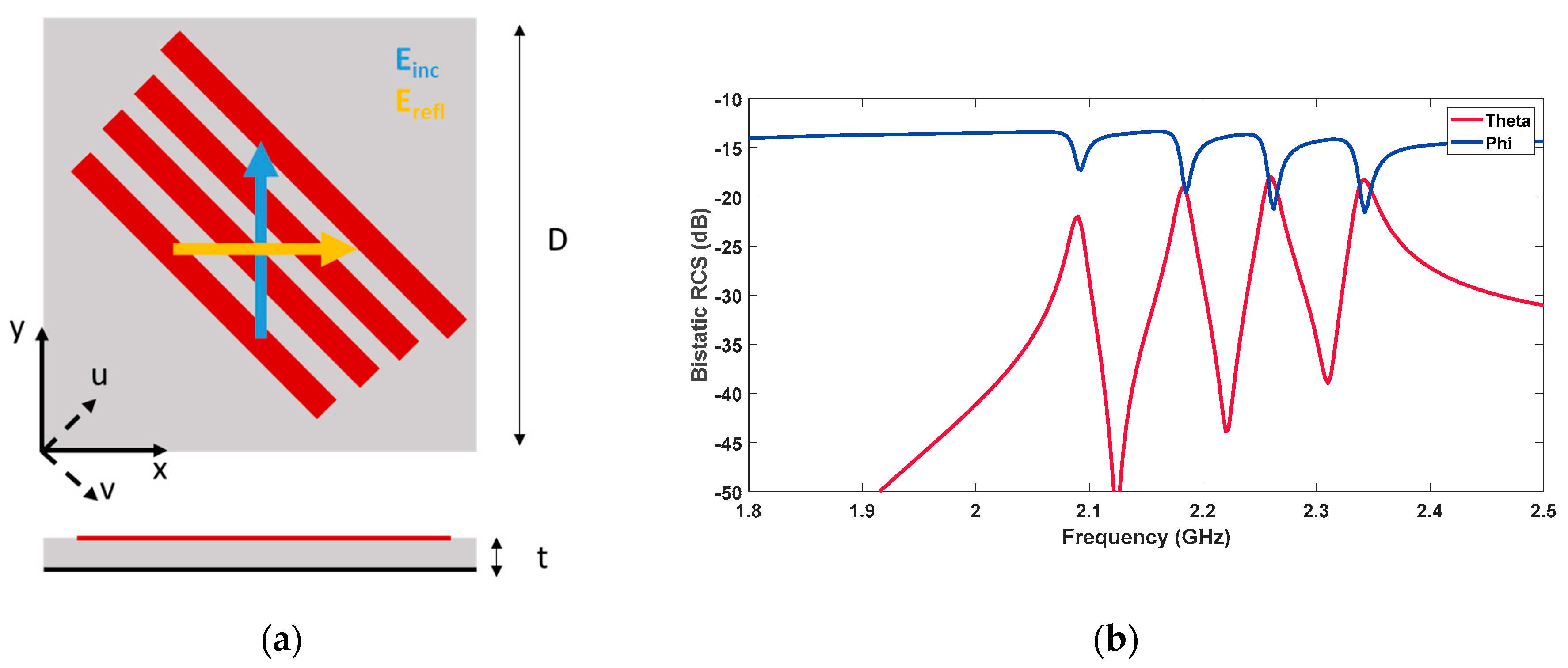
Some depolarizing tags have been designed and fabricated to characterize the performance of the reader. The tags are formed by a series of dipoles of different length placed at an adequate distance from a metallic ground plane. The two-layer surface acts as a multi-frequency polarization converter [14,15]. The device is able to convert the polarization of the impinging wave only when the angle of incidence is close to 45° with respect to the orientation of the dipole.
The unit cell that has been selected for the design of the multi-frequency polarization converter is reported in Figure 4. The dipoles are printed on a thin FR4 slab of 0.2 mm and glued on a Rohacell spacer, t, of 3 mm, which is backed by a metallic ground plane. The size of the resonator, D, is equal to 67 mm. The polarization converter stack-up is reported in the same figure. By modifying the length of the dipoles, it is possible to select the working frequencies of the polarization converter. The physical mechanism of the linear polarization converter can be described by considering the additional coordinates system that originated from the two perpendicular symmetric axes u and v, which are rotated 45° with respect to the y axis, as shown in the Figure. After the decomposition into u and v components, the incident electric field E i n c can be written as follows:
E i n c = E 0 y ^ = E 0 / 2 u ^ + E 0 / 2 v ^
Indicating with Ru and Rv the reflection coefficient in the uv-coordinates system, the reflected electric field can be consequently, the reflected electric field E r e f l can be written as follows:
E r e f l = R u E 0 / 2 u ^ + R v E 0 / 2 v ^
According to relation (2), E r e f l will be parallel to the x-axis if the following conditions are met:
R u = 1 ,   R v = 1
The conditions in (3) are met at the resonance frequency of the dipole-ground plane structure where the reflection coefficient along the dipole (Ru) is characterized by a phase crossing the zero, and the reflection coefficient orthogonal to the dipole (Rv) is characterized by a phase of 180°. In order to guarantee that the Ru and Rv needs to be equal or very close to 1, a dielectric substrate with a very low tangent loss is required. For this reason, a Rohacell spacer is used. The frequency response of the investigated structure has initially been analyzed as an infinitely periodic one for assessing the effect of the resonators by using a Periodic Method of Moments (PMoM) [16]. Afterwards, a simulation of the single unit cell was carried out by Ansys HFSS v.18. Both the co-polar and cross-polar RCS of the tag is reported in Figure 4b.

4. Reader Antennas

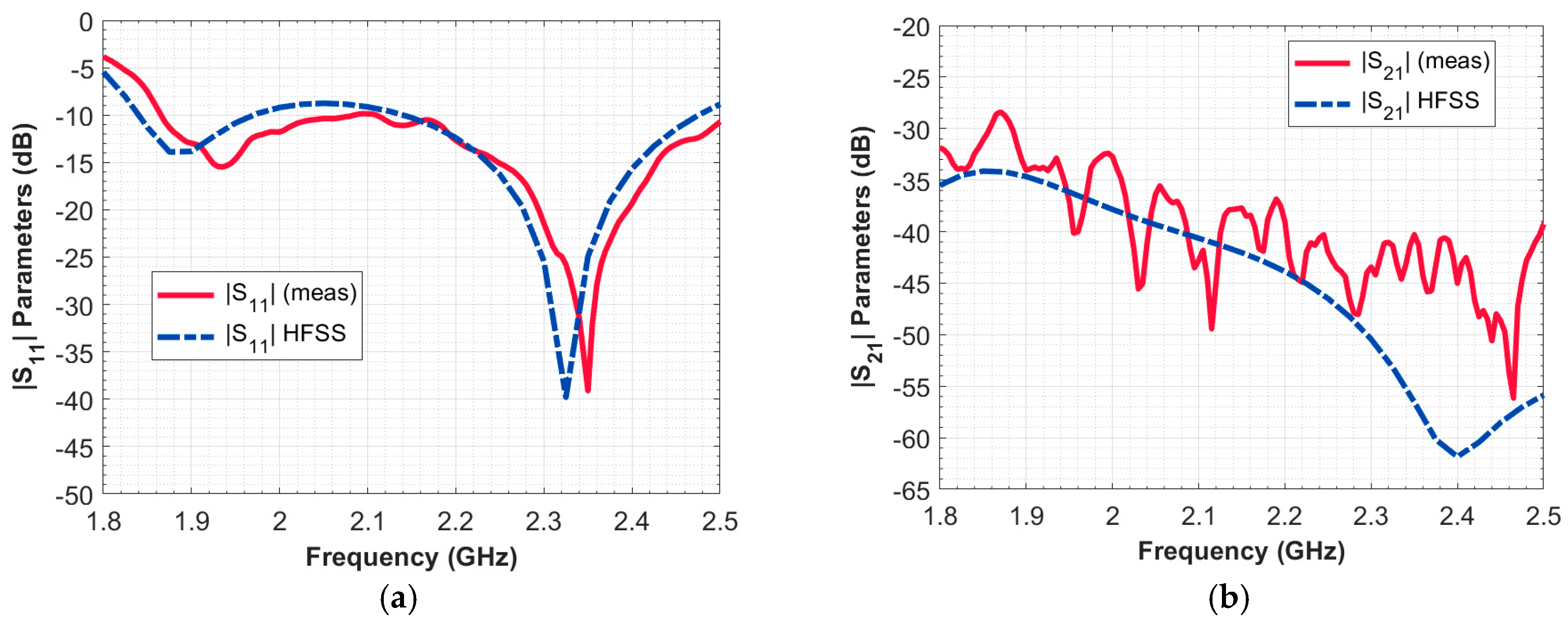
The designed tag encodes data into the frequency spectrum by resorting to resonant structures. The resonant structure operates in the (1.9–2.5) GHz Band. The design encodes the information in the cross-polar scattering as the tag is also working on metallic objects [17]. A typical drawback of frequency domain tag is the need of a large spectrum for data encoding. In order to obtain reliable RCS measurements, wideband and compact wideband antennas need to be designed. The main objectives of the project have therefore been to guarantee, in the whole band in which the tag information is encoded, a high level of gain and, at the same time, a very low level of coupling between the two antennas (i.e., low value of the S 21 scattering parameter). The overall system, as shown in Figure 5, consists of two radiating elements, namely two wideband E-Shaped Antennas printed on a 0.2 mm thick FR4 substrate and placed at a distance of 15 mm from the ground plane [18]. The aim of the project has also been to optimize the size of the radiators in order to obtain a compact structure. The configuration consists of two orthogonal antennas, one transmitting and one receiving, with both operating in linear polarization, in order to reliably retrieve the cross-polar component backscattered from the tag when it is interrogated. In this way, it is possible to distinguish the RCS of the cross-polar component of the tag from that of the clutter in the real scenario, because the latter has a dominant frequency response in the co-polar component. To achieve this goal, or at least to ensure an isolation between −30 dB and −50 dB in the analyzed frequency range, the distance at which the two antennas can be positioned on the FR4 substrate was numerically optimized using Ansys HFSS software. In addition, once this optimal distance was found, to provide a further lowering of S 21 , a structure consisting of a thin metallic slab was introduced and suitably dimensioned. As evidence of this point, the curves of | S 21 | are shown in Figure 6 and overlapped in two different cases: The former refers to the configuration with the metallic wall and the latter to the same configuration as the first but without this metallic slab. As we can see, for all the frequencies of interest, the trend in the former case is always lower than the other, and the lowering of the | S 21 | level improves as the frequency increases. The information encoded in the tag is contained in the spectrum of the cross-polar component of the RCS that is between 1.9 GHz and 2.5 GHz, so a simple patch antenna configuration is not a good solution to obtain this purpose because it is a narrow bandwidth. The method employed to increase the bandwidth is based on the insertion of two parallel slots into the antenna patch, so by modifying the length, width, and position of these slots, one can obtain a bandwidth up to 30%, which guarantees the desired performance; moreover, as shown in the Figure 6b, it is possible to obtain a Realized Gain that is always higher than 8 dB in the bandwidth of interest. Radiation patterns of the two principal planes have been obtained through simulation with Ansoft HFSS and are shown in Figure 7a,b, respectively. To verify the correct behaviour of the E-shaped patch antenna, the simulated scattering parameters were compared with the measurements carried out by using a Keysight network analyzer in a non-anechoic environment, which was the Microwave Laboratory of the department of Information Engineering at the University of Pisa. As is evident from Figure 8, the value of the measured S 11 module is always less than −10dB from 1.9 to 2.5 (GHz); the behaviour of the | S 21 | is also consistent with respect to the simulated curve, as it always remains below −35 dB and improves as the frequency increases. The slight discrepancies between the measurement and simulations of scattering parameters is attributed to fabrication and assembly tolerances. The specific antenna geometry is shown in Figure 5. The single radiating element is a traditional wide-band microstrip antenna, where the patch size is characterized by ( L ,   W ,   h _ a i r ) and it is fed by a coaxial probe at position ( X f , Y f ) . Two parallel slots are placed into the E-shaped patch symmetrically with respect to the feed point. The slot length ( L S ) , width ( W S ) , and position ( P S ) are important parameters in achieving the desired performances. Various simulations were therefore carried out to jointly optimize these values; in particular, the obtained antenna parameters are listed below (in millimeters):
( L , W ) = ( 70 , 50 ) , h _ a i r = 15 , ( X f , Y f ) = ( 35 , 6 ) , ( L S , W S ) = ( 40 , 6.6 ) , P S = 9 , p a t c h _ o f f s e t = 70
From Figure 8a, it can be observed that the antenna has two resonant frequencies: 1.93 GHz and 2.35 GHz. The antenna frequency band with −10 dB return loss covers the frequency range of 1.86–2.5 GHz. It has a bandwidth of 29.36% with a center frequency of 2.18 GHz. This particularly high bandwidth is achieved by combining patch and slot effects. Indeed, the antenna width W controls the higher resonant frequency, while the slots control the lower resonant frequency.

5. Experiments

This section is dedicated to the experimental verification of the reader. In particular, the frequency response of the designed four-bit tags was measured in a non-anechoic environment at a distance of 20 cm. Calibration with the background was not necessary since the measured signal level was sufficiently higher than the antenna coupling. The maximum read range of this non-compensated measurement approach is directly related to the antenna coupling level which, for our antennas, was kept below −35 dB in all the analyzed frequency bands. The measurement setup is shown in Figure 9. In Figure 10, the spectral response measured with the reader is compared with the VNA connected to the readers’ antennas. The agreement between the curves is satisfactory as the portable reader is capable of detecting the four frequency peaks even if there are some small disagreements on the measured level of backscattered signals.

6. Discussion

Further proof of the practical easiness and convenience in the adoption of the proposed reader can be inferred from the comparison reported in Table 2, where the performance and cost of some available chipless RFID readers are summarized.

7. Conclusions

In this paper, the architecture for a low-cost chipless reader has been presented, fabricated, and experimentally verified. The reader operates in the frequency band of 2–2.5 GHz and is equipped with two wideband and low-profile antennas. The reader is completely integrated in a single board, and its cost for a volume of 1 k pcs is around $120. The reader antennas consist of two orthogonally placed E-shaped patch arrays, and the coupling is maintained below −35 dB. The reader operates in cross-polarization and has been tested with some depolarizing tags composed of four oblique dipoles. The agreement between the results provided by a VNA and the proposed reader is satisfactory.

Author Contributions

L.B. and L.M. developed the reader. F.C. and S.T. designed the chipless tags. S.T., S.G. and F.C. designed the reader antennas. L.B., L.M., S.G., F.C. and S.T. performed measurements. F.C., S.T., L.B., L.M. prepared the manuscript. G.M. coordinated the project and revised the manuscript.

Funding

This research was partially funded by H2020 Programme, Call MSCA-RISE-2014, Project EMERGENT, GA n. 645771.

Conflicts of Interest

The authors declare no conflict of interest. The founding sponsors had no role in the design of the study; in the collection, analyses, or interpretation of data; in the writing of the manuscript, and in the decision to publish the results.

References

  1. Ramos, A.; Girbau, D.; Lazaro, A.; Villarino, R. Wireless Concrete Mixture Composition Sensor Based on Time-Coded UWB RFID. IEEE Microw. Wirel. Compon. Lett. 2015, 25, 681–683. [Google Scholar]
  2. Costa, F.; Genovesi, S.; Monorchio, A. A Chipless RFID Based on Multiresonant High-Impedance Surfaces. IEEE Trans. Microw. Theory Tech. 2013, 61, 146–153. [Google Scholar] [CrossRef]
  3. Vena, A.; Perret, E.; Tedjini, S. Chipless RFID Tag Using Hybrid Coding Technique. IEEE Trans. Microw. Theory Tech. 2011, 59, 3356–3364. [Google Scholar] [CrossRef]
  4. Preradovic, S.; Karmakar, N.C. Design of short range chipless RFID reader prototype. In Proceedings of the 2009 International Conference on Intelligent Sensors, Sensor Networks and Information Processing (ISSNIP), Melbourne, Australia, 7–10 December 2009; pp. 307–312. [Google Scholar]
  5. Vithalkar, A. Chipless RFID reader. Bachelor’s Thesis, Delhi University, New Delhi, India, 18 April 2018. [Google Scholar]
  6. Preradovic, S.; Karmakar, N.C. Multiresonator based chipless RFID tag and dedicated RFID reader. In Proceedings of the 2010 IEEE MTT-S International Microwave Symposium, Anaheim, CA, USA, 23–28 May 2010; pp. 1520–1523. [Google Scholar]
  7. Koswatta, R.V.; Karmakar, N.C. A Novel Reader Architecture Based on UWB Chirp Signal Interrogation for Multiresonator-Based Chipless RFID Tag Reading. IEEE Trans. Microw. Theory Tech. 2012, 60, 2925–2933. [Google Scholar] [CrossRef]
  8. Karmakar, N.C.; Koswatta, R.; Kalansuriya, P.; E-Azim, R. Chipless RFID Reader Architecture; Artech House: Norwood, MA, USA, 2013; ISBN 978-1-60807-561-4. [Google Scholar]
  9. Garbati, M.; Siragusa, R.; Perret, E.; Halopé, C. Low cost low sampling noise UWB Chipless RFID reader. In Proceedings of the 2015 IEEE MTT-S International Microwave Symposium, Phoenix, AZ, USA, 17–22 May 2015; pp. 1–4. [Google Scholar]
  10. Garbati, M.; Perret, E.; Siragusa, R. Chipless RFID Reader Design for Ultra-Wideband Technology: Design, Realization and Characterization; Elsevier: Oxford, UK, 2018; ISBN 978-0-08-102761-5. [Google Scholar]
  11. Lázaro, A.; Villarino, R.; Costa, F.; Genovesi, S.; Gentile, A.; Buoncristiani, L.; Girbau, D. Chipless Dielectric Constant Sensor for Structural Health Testing. IEEE Sens. J. 2018, 18, 5576–5585. [Google Scholar] [CrossRef]
  12. XeThru Shop. Single-Chip Radar Sensor with Sub-mm Resolution—XeThru. Available online: https://shop.xethru.com/ (accessed on 4 December 2018).
  13. UWB Radar|UWB Sensor|2D ISAR|3D ISAR|RCS Systems|UWB Antenna|Delay Line. Available online: http://www.geozondas.com/main_page.php?pusl=5 (accessed on 4 December 2018).
  14. Borgese, M.; Costa, F.; Genovesi, S.; Monorchio, A.; Manara, G. Multi-frequency polarizarition converter with enhanced angular robustness. In Proceedings of the 2016 IEEE International Symposium on Antennas and Propagation (APSURSI), Fajardo, Puerto Rico, 26 June–1 July 2016; pp. 669–670. [Google Scholar]
  15. Borgese, M.; Costa, F.; Genovesi, S.; Monorchio, A.; Manara, G. Optimal Design of Miniaturized Reflecting Metasurfaces for Ultra—Wideband and Angularly Stable Polarization Conversion. Sci. Rep. 2018, 8, 7651. [Google Scholar] [CrossRef]
  16. Mittra, R.; Chan, C.H.; Cwik, T. Techniques for analyzing frequency selective surfaces—A review. Proc. IEEE 1988, 76, 1593–1615. [Google Scholar] [CrossRef]
  17. Costa, F.; Gentile, A.; Genovesi, S.; Buoncristiani, L.; Lazaro, A.; Villarino, R.; Girbau, D. A Depolarizing Chipless RF Label for Dielectric Permittivity Sensing. IEEE Microw. Wirel. Compon. Lett. 2018, 28, 371–373. [Google Scholar] [CrossRef]
  18. Yang, F.; Zhang, X.-X.; Ye, X.; Rahmat-Samii, Y. Wide-band E-shaped patch antennas for wireless communications. IEEE Trans. Antennas Propag. 2001, 49, 1094–1100. [Google Scholar] [CrossRef]
  19. Blischak, A.T.; Manteghi, M. Embedded Singularity Chipless RFID Tags. IEEE Trans. Antennas Propag. 2011, 59, 3961–3968. [Google Scholar] [CrossRef]
  20. Garbati, M.; Siragusa, R.; Perret, E.; Halopé, C. Impact of an IR-UWB Reading Approach on Chipless RFID Tag. IEEE Microw. Wirel. Compon. Lett. 2017, 27, 678–680. [Google Scholar] [CrossRef]
  21. Buchanan, N.B.; Fusco, V. Single VCO chipless RFID near-field reader. Electron. Lett. 2016, 52, 1958–1960. [Google Scholar] [CrossRef] [Green Version]
Figure 1. Architecture of the portable reader for frequency domain chipless tags.
Electronics 08 00035 g001
Figure 2. Portable reader developed for frequency domain chipless tags. (a) 3D Rendering, (b) Printed Circuit Board Assembled.
Electronics 08 00035 g002
Figure 3. Firmware sequences of the portable reader for frequency domain chipless tags.
Electronics 08 00035 g003
Figure 4. Simulated frequency response of a 1 × 1 tag.
Electronics 08 00035 g004
Figure 5. Geometry of a wide-band E-shaped antenna consisting of two parallel slots in the patch. (a) Top view, (b) side view, (c) antenna prototypes.
Electronics 08 00035 g005
Figure 6. (a) Simulated | S 21 | of the E-shaped patch antenna. Comparison between the adopted configuration (with a metallic slab) and the one without the latter. (b) Calculated Realized Gain (dB) of the E-shaped patch antenna versus the frequency.
Electronics 08 00035 g006
Figure 7. Cross-pol radiation patterns calculated at the frequencies 1.9, 2.2, and 2.5 GHz respectively. (a) Radiation pattern on the φ = 0 ° , (b) φ = 90 ° .
Electronics 08 00035 g007
Figure 8. Comparison between simulated and measured scattering parameters of the E-shaped patch antenna. On the left (a) is shown | S 11 | vs. frequency, on the right (b) | S 21 | vs. frequency.
Electronics 08 00035 g008
Figure 9. Measurement setup.
Electronics 08 00035 g009
Figure 10. Measured response of the four-bit depolarizing tag; comparison between the portable chipless reader and the VNA (Vector Network Analyzer).
Electronics 08 00035 g010
Table 1. Costs of the reader for a production of 1 k pcs.
Analog/Digital Control SectionRF Tx ChannelRF Rx Channel
Microprocessor R5F5631ECDFB: $8.2Pwr Divider BP2U1+: $1.05Antenna: $15
DAC LTC7545ABSW#PBF: $4.3RF Amp PGA-105+: $1.55RF Amp PGA-105+: $1.55
VCO ROS-2490C+: $17.3Antenna: $15PG Detector AD8302ARUZ: $12.5
ADC AD7472ARUZ: $9.9Passive components + other: $7.7Passive components + other: $2.95
PCB + Passive components + other: $2.3Assembling + functional test: 9.7$Assembling + functional test: 8$
Assembling + functional test: $3
Total: $45Total: $35Total: $40
Total costs for 1 K pcs: $120
Table 2. Performance and cost comparison of chipless RFID tag readers.
Reference[7][19][20][21]This work
Operating bandwidth4–8 GHz50–20.5 GHz3.1–10.6GHz2.4–3.4 GHz2–2.5 GHz
Reader systemPCB circuitVNA-basedPCB circuitVCO, oscilloscope, ramp generatorPCB circuit
Cost<$650high<2.5 Keuro (antenna not included)medium$120 (antenna included)
# of reference measurementsNo need of a reference measurementsReference measurements requiredNo need of a reference measurementsReference measurements requiredNo need of a reference measurements