Sub-Milliwatt Transceiver IC for Transcutaneous Communication of an Intracortical Visual Prosthesis
Abstract
:1. Introduction
2. System Requirements and Considerations
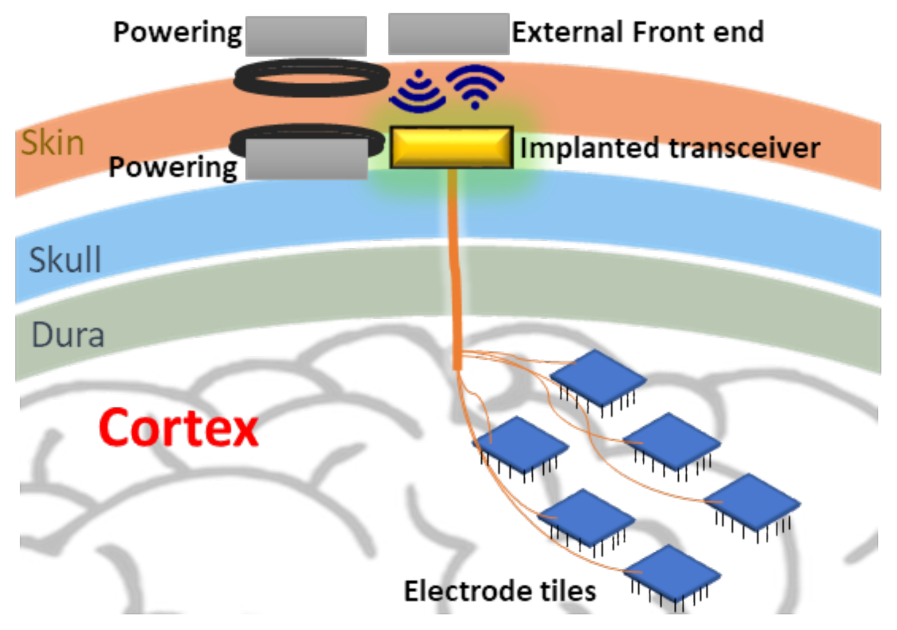
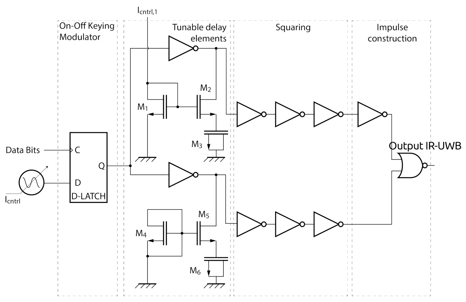
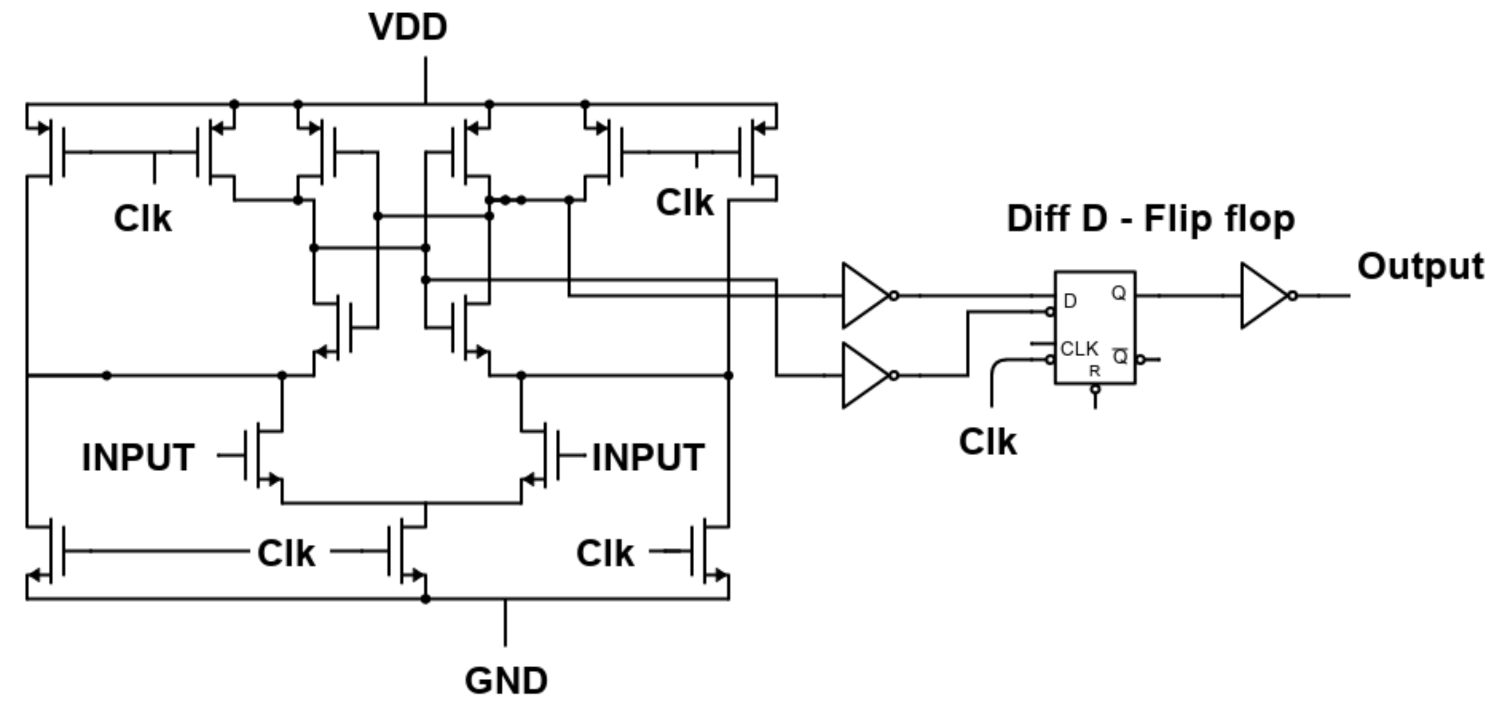
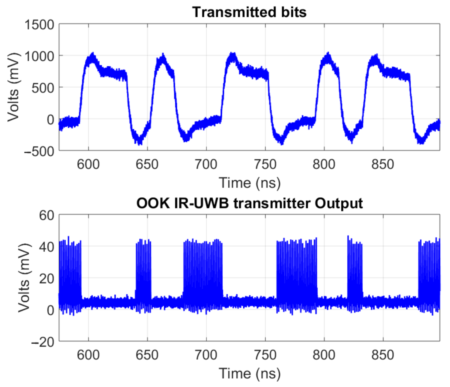
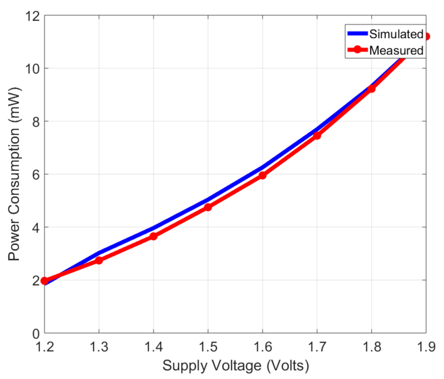
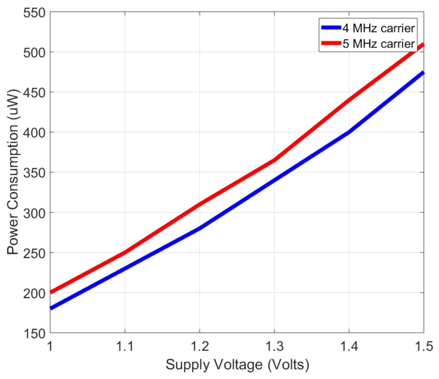
- Power consumption: Based on power consumption reported in [11,20], the projected power consumption of the implant side of the 1024 electrode visual prosthesis without a wireless interface is in the order of 100 mW. Considering the wireless power transfer, and possible battery constraints at the implant side, it is desired that the wireless system adds no more than 10–30% extra power to the power budget at the implant side. This implies that only a low-power solution for the implanted transceiver will create a viable system. The external transceiver above the skin will be allowed to consume more power. Our proposed non-coherent BPSK receiver will fulfill this due to its simple architecture and predominantly digital components. For the uplink, on-off keying (OOK) is used for the IR-UWB transmitter because of its simpler architecture making for a low-power transmitter.
- Transmission data rate: It is required to transmit a minimum of 23 Mbps for compressed data with electrode recordings [13]. The receiver is required to handle a minimum of 200 kbps of stimulation data [19]. IR-UWB for the uplink has the potential to deliver high data rate for short distances. Using an inductively-coupled link with BPSK at low frequency will provide a sufficient data rate, while yielding a low-power solution [21].
- Bit-error-rate (BER): the uplink and downlink system should give a BER of at least 10 over the full communication chain with an external side. BPSK is used for the downlink because it has a better theoretical bit error rate performance than other modulation schemes, such as amplitude shift keying and frequency shift keying [22]. The BER target is checked by using the IC results in the overall link budget. The focus of this work is on a low-power implanted side transceiver IC. Any need for improved BER could be taken care of by adjusting the link budget through the coil design with the external side. The case of the uplink, for example, where the IR-UWB receiver is external, reported receivers [23,24] at similar sensitivities already meet the BER target of 10. Similarly, for the downlink case, where the transmitter is external, the transmit voltage can be scaled easily to meet the implanted receiver sensitivity of 50 mV. In addition, straightforward coil design can already realize the required channel bandwidth.
- Security: with the increasing risk of communication security breaches, the wireless link needs to be secure, especially at the physical layer. Therefore, short range transcutaneous communication is proposed from beneath the skin to the receiver just outside the head. The expected transmission path through skin is expected to be in the range of 3–7 mm [25].
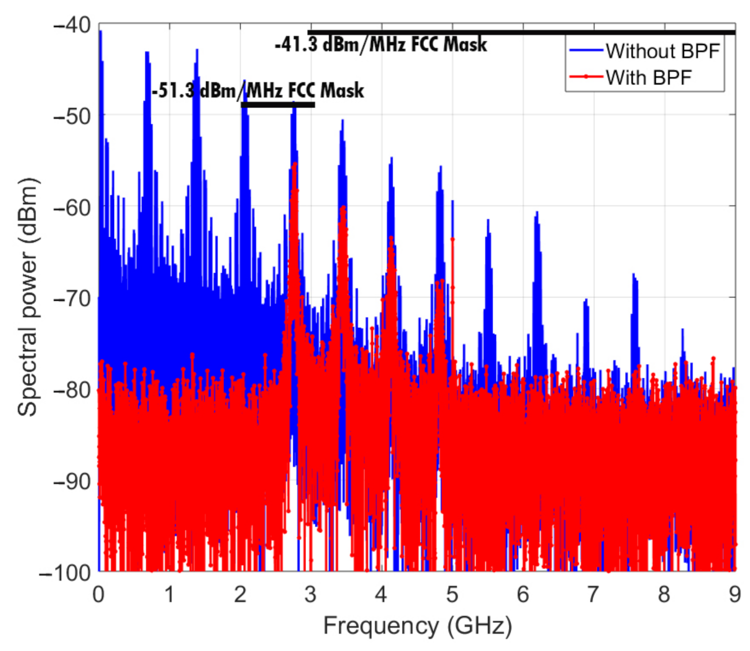
- Co-existence with other sub-systems: in the overall wireless system of the visual prosthesis, the downlink and wireless powering are also present. The wireless link should be able to cope with other sub-systems in terms of frequency spectrum use, interference, and cross talk. Using the 3–5 GHz band for the uplink and the 4–12 MHz band for downlink provides sufficient frequency spacing to avoid interference. In addition, we propose the use of a coupled inductive link. Furthermore, the lower 3–5 GHz band of the 3–10 GHz for UWB is preferred due to lower attenuation through the skin [9]. In principle, pulse-based systems like IR-UWB are carrierless, and our target frequency band is 3–5 GHz as opposed to a carrier frequency, which is about 4–12 MHz for the BPSK communication in the downlink. Interference will be minimal due to its localization and near-field nature.
3. Implanted Transceiver
3.1. IR-UWB Transmitter
3.2. Non-Coherent BPSK Receiver
4. Measurement Setup
4.1. Test IC
4.2. Demonstrator Board
4.3. Experimental Test Setup
5. Results
5.1. IR-UWB Transmitter
5.1.1. IC Measurement Results
5.1.2. Link Budget for Uplink
5.2. Non-Coherent BPSK Receiver
5.2.1. IC Measurement Results
5.2.2. Link Budget for Downlink
6. Discussion
6.1. Comparison with the State of the Art
6.2. Medical Safety
7. Conclusions
Author Contributions
Funding
Data Availability Statement
Acknowledgments
Conflicts of Interest
Abbreviations
| ISM | Industrial, Scientific, and Medical |
| IC | Integrated Circuit |
| SAR | Specific Absorption Rate |
| NESTOR | NEuronal STimulation for Recovery of Function |
| BPSK | Binary Phase Shift Keying |
| PLL | Phase Locked Loop |
| FSK | Frequency Shift Keying |
| ASK | Amplitude Shift Keying |
| BER | Bit Error Rate |
| CMOS | Complementary Metal–Oxide–Semiconductor |
| SPST | Single Pole Single Throw |
| IR-UWB | Impulse Radio Ultra Wide Band |
| OOK | On-Off Keying |
| DDM | Differential detection method |
| BLE | Bluetooth Low Energy |
| HBC | Human body communication |
| TTC | Transmission time control |
| P-OFDM | Pseudo orthogonal frequency-division multiplexing |
| RFIC | Radio Frequency Integrated Circuits |
| ADC | Analog to Digital Converter |
References
- Pascolini, D.; Mariotti, S.P. Global estimates of visual impairment: 2010. Br. J. Ophthalmol. 2012, 96, 614–618. [Google Scholar] [CrossRef] [Green Version]
- Bourne, R.R.A.; Flaxman, S.R.; Braithwaite, T. Magnitude, temporal trends, and projections of the global prevalence of blindness and distance and near vision impairment: A systematic review and meta-analysis. Lancet Glob. Health 2017, 5, e888–e897. [Google Scholar] [CrossRef] [Green Version]
- Dobelle, W.H. Artificial Vision for the Blind by Connecting a Television Camera to the Visual Cortex. ASAIO J. 2000, 46, 3–9. [Google Scholar] [CrossRef] [PubMed] [Green Version]
- NESTOR. Neuronal Stimulation for Recovery of Function. Available online: https://nestor-sight.com/ (accessed on 15 August 2021).
- Chen, X.; Wang, F.; Fernandez, E.; Roelfsema, P.R. Shape perception via a high-channel-count neuroprosthesis in monkey visual cortex. Science 2020, 370, 1191–1196. [Google Scholar] [CrossRef] [PubMed]
- Yin, M.; Borton, D.A.; Aceros, J.; Patterson, W.R.; Nurmikko, A.V. A 100-Channel Hermetically Sealed Implantable Device for Chronic Wireless Neurosensing Applications. IEEE Trans. Biomed. Circuits Syst. 2013, 7, 115–128. [Google Scholar] [CrossRef] [Green Version]
- Coulombe, J.; Sawan, M.; Gervais, J.F. A Highly Flexible System for Microstimulation of the Visual Cortex: Design and Implementation. IEEE Trans. Biomed. Circuits Syst. 2007, 1, 258–269. [Google Scholar] [CrossRef]
- Lowery, A.J.; Rosenfeld, J.V.; Lewis, P.M.; Browne, D.; Mohan, A.; Brunton, E.; Yan, E.; Maller, J.; Mann, C.; Rajan, R.; et al. Restoration of vision using wireless cortical implants: The Monash Vision Group project. In Proceedings of the 2015 37th Annual International Conference of the IEEE Engineering in Medicine and Biology Society (EMBC), Milan, Italy, 25–29 August 2015; pp. 1041–1044. [Google Scholar] [CrossRef]
- Bahrami, H.; Gosselin, B.; Rusch, L.A. Realistic modeling of the biological channel for the design of implantable wireless UWB communication systems. In Proceedings of the 2012 Annual International Conference of the IEEE Engineering in Medicine and Biology Society, San Diego, CA, USA, 28 August–1 September 2012; pp. 6015–6018. [Google Scholar] [CrossRef]
- Liu, T.; Bihr, U.; Becker, J.; Anders, J.; Ortmanns, M. In vivo verification of a 100 Mbps transcutaneous optical telemetric link. In Proceedings of the 2014 IEEE Biomedical Circuits and Systems Conference (BioCAS) Proceedings, Lausanne, Switzerland, 22–24 October 2014; pp. 580–583. [Google Scholar] [CrossRef]
- Chae, M.S.; Yang, Z.; Yuce, M.R.; Hoang, L.; Liu, W. A 128-Channel 6 mW Wireless Neural Recording IC With Spike Feature Extraction and UWB Transmitter. IEEE Trans. Neural Syst. Rehabil. Eng. 2009, 17, 312–321. [Google Scholar] [CrossRef] [PubMed]
- Mirbozorgi, S.A.; Bahrami, H.; Sawan, M.; Rusch, L.A.; Gosselin, B. A Single-Chip Full-Duplex High Speed Transceiver for Multi-Site Stimulating and Recording Neural Implants. IEEE Trans. Biomed. Circuits Syst. 2016, 10, 643–653. [Google Scholar] [CrossRef] [PubMed]
- Omisakin, A.; Mestrom, R.M.C.; Bentum, M.J. System Design of a Low-power Wireless Link for Neural Recording in a Visual Prosthesis. In Proceedings of the 2019 IEEE AFRICON, Accra, Ghana, 25–27 September 2019. [Google Scholar]
- Toledo, P.; Rubino, R.; Musolino, F.; Crovetti, P. Re-Thinking Analog Integrated Circuits in Digital Terms: A New Design Concept for the IoT Era. IEEE Trans. Circuits Syst. II Express Briefs 2021, 68, 816–822. [Google Scholar] [CrossRef]
- Staszewski, R.B. Digital RF and digitally-assisted RF (invited). In Proceedings of the 2011 IEEE International Symposium on Radio-Frequency Integration Technology, Beijing, China, 30 November–2 December 2011; pp. 9–16. [Google Scholar] [CrossRef]
- Zhou, M.; Liu, W. A Non-Coherent PSK Receiver with Interference-Canceling for Transcutaneous Neural Implants. In Proceedings of the 2007 IEEE International Solid-State Circuits Conference, Digest of Technical Papers, San Francisco, CA, USA, 11–15 February 2007; pp. 156–593. [Google Scholar] [CrossRef]
- Kiani, M.; Ghovanloo, M. A 13.56-Mbps Pulse Delay Modulation Based Transceiver for Simultaneous Near-Field Data and Power Transmission. IEEE Trans. Biomed. Circuits Syst. 2015, 9, 1–11. [Google Scholar] [CrossRef]
- Zgaren, M.; Sawan, M. A Low-Power Dual-Injection-Locked RF Receiver With FSK-to-OOK Conversion for Biomedical Implants. IEEE Trans. Circuits Syst. I: Regul. Pap. 2015, 62, 2748–2758. [Google Scholar] [CrossRef]
- Omisakin, A.; Mestrom, R.; Bentum, M. Low-Power Communication for an Implanted Intracortical Visual Prosthesis. In Proceedings of the 2019 13th European Conference on Antennas and Propagation (EuCAP), Krakow, Poland, 31 March–5 April 2019; pp. 1–4. [Google Scholar]
- Shahrokhi, F.; Abdelhalim, K.; Serletis, D.; Carlen, P.L.; Genov, R. The 128-Channel Fully Differential Digital Integrated Neural Recording and Stimulation Interface. IEEE Trans. Biomed. Circuits Syst. 2010, 4, 149–161. [Google Scholar] [CrossRef] [PubMed] [Green Version]
- Omisakin, A.; Mestrom, R.; Bentum, M. Low-Power BPSK Inductive Data Link for an Implanted Intracortical Visual Prosthesis. In Proceedings of the 2019 41st Conference on Engineering in Medicine and Biology EMBC, Berlin, Germany, 23–27 July 2019. [Google Scholar]
- Couch, L.W. Digital and Analog Communication Systems, 8th ed.; Prentice Hall: Hoboken, NJ, USA, 2012. [Google Scholar]
- Ebrazeh, A.; Mohseni, P. 30 pJ/b, 67 Mbps, Centimeter-to-Meter Range Data Telemetry With an IR-UWB Wireless Link. IEEE Trans. Biomed. Circuits Syst. 2015, 9, 362–369. [Google Scholar] [CrossRef]
- Zhang, Z.; Li, Y.; Mouthaan, K.; Lian, Y. A Miniature Mode Reconfigurable Inductorless IR UWB Transmitter Receiver for Wireless Short Range Communication and Vital Sign Sensing. IEEE J. Emerg. Sel. Top. Circuits Syst. 2018, 8, 294–305. [Google Scholar] [CrossRef]
- Delbeke, J.; Veraart, C. Visual Prostheses. In Encyclopedia of Medical Devices and Instrumentation, 2nd ed.; John Wiley & Sons, Inc.: Hoboken, NJ, USA, 2006; pp. 530–549. [Google Scholar]
- Wentzloff, D. Pulse-Based Ultra-Wideband Transmitters for Digital Communication. Ph.D. Thesis, Massachusetts Institute of Technology, Cambridge, MA, USA, 2007. [Google Scholar]
- Federal Communications Commission. FCC First Report and Order 02-48; Technical Report; Federal Communications Commission: Washington, DC, USA, 2002. [Google Scholar]
- Yoon, C.; Lee, J.; Park, Y.; Park, H.; Kim, J.; Pak, J.S.; Kim, J. Design of a Low-Noise UWB Transceiver SiP. IEEE Des. Test Comput. 2008, 25, 18–28. [Google Scholar] [CrossRef]
- Suman, S.; Sharma, K.G.; Ghosh, P.K. Analysis and design of current starved ring VCO. In Proceedings of the 2016 International Conference on Electrical, Electronics, and Optimization Techniques (ICEEOT), Chennai, India, 3–5 March 2016; pp. 3222–3227. [Google Scholar] [CrossRef]
- Nguyen, C.; Miao, M. Design of CMOS RFIC Ultra-Wideband Impulse Transmitters and Receivers; Springer: Cham, Switzerland, 2017. [Google Scholar] [CrossRef]
- Miao, M.; Nguyen, C. On the Development of an Integrated CMOS-Based UWB Tunable-Pulse Transmit Module. IEEE Trans. Microw. Theory Tech. 2006, 54, 3681–3687. [Google Scholar] [CrossRef]
- Weste, N.; Harris, D. CMOS VLSI Design: A Circuits and Systems Perspective, 4th ed.; Addison-Wesley Publishing Company: Boston, MA, USA, 2010. [Google Scholar]
- Puers, R.; Thoné, J. Short Distance Wireless Communications. In Bio-Medical CMOS ICs; Yoo, H.J., van Hoof, C., Eds.; Springer: Boston, MA, USA, 2011. [Google Scholar] [CrossRef]
- Omisakin, A.; Mestrom, R.M.C.; Bentum, M.J. Low-Power Wireless Data Transfer System for Stimulation in an Intracortical Visual Prosthesis. Sensors 2021, 21, 735. [Google Scholar] [CrossRef]
- Asgarian, F.; Sodagar, A.M. A high-data-rate low-power BPSK demodulator and clock recovery circuit for implantable biomedical devices. In Proceedings of the 2009 4th International IEEE/EMBS Conference on Neural Engineering, Antalya, Turkey, 29 April–2 May 2009; pp. 407–410. [Google Scholar] [CrossRef]
- Cenci, P.; Bolatkale, M.; Rutten, R.; Lassche, G.; Makinwa, K.; Breems, L. A 28 nm 2 GS/s 5-b single-channel SAR ADC with gm-boosted StrongARM comparator. In Proceedings of the ESSCIRC 2017—43rd IEEE European Solid State Circuits Conference, Leuven, Belgium, 11–14 September 2017; pp. 171–174. [Google Scholar] [CrossRef]
- Diligent Inc. Analog Discovery 2; Diligent Corporation: New York, NY, USA, 2015. [Google Scholar]
- Teledyne LeCroy. WaveMaster 8 Zi-B Oscilloscopes 4–30 GHz; Teledyne LeCroy: Chestnut Ridge, NY, USA, 2019. [Google Scholar]
- Liu, D.; Geng, S.; Rhee, W.; Wang, Z. A high efficiency robust IR-UWB receiver design for high data rate CM-range communications. In Proceedings of the 2014 IEEE International Symposium on Circuits and Systems (ISCAS), Melbourne, VIC, Australia, 1–5 June 2014; pp. 1901–1904. [Google Scholar] [CrossRef]
- Kuo, F.; Binsfeld Ferreira, S.; Chen, H.R.; Cho, L.; Jou, C.; Hsueh, F.; Madadi, I.; Tohidian, M.; Shahmohammadi, M.; Babaie, M.; et al. A Bluetooth Low-Energy Transceiver with 3.7-mW All-Digital Transmitter, 2.75-mW High-IF Discrete-Time Receiver, and TX/RX Switchable On-Chip Matching Network. IEEE J. Solid-State Circuits 2017, 52, 1144–1162. [Google Scholar] [CrossRef] [Green Version]
- Liu, D.; Ni, X.; Zhou, R.; Rhee, W.; Wang, Z. A 0.42-mW 1-Mb/s 3- to 4-GHz Transceiver in 0.18 um CMOS With Flexible Efficiency, Bandwidth, and Distance Control for IoT Applications. IEEE J. Solid-State Circuits 2017, 52, 1479–1494. [Google Scholar] [CrossRef]
- Teng, K.; Heng, C. A 370-pJ/b Multichannel BFSK/QPSK Transmitter Using Injection-Locked Fractional-N Synthesizer for Wireless Biotelemetry Devices. IEEE J. Solid-State Circuits 2017, 52, 867–880. [Google Scholar] [CrossRef]
- Lee, S.; Song, K.; Yoo, J.; Yoo, H.J. A Low-Energy Inductive Coupling Transceiver With Cm-Range 50-Mbps Data Communication in Mobile Device Applications. IEEE J. Solid-State Circuits 2010, 45, 2366–2374. [Google Scholar] [CrossRef]
- Maity, S.; Chatterjee, B.; Chang, G.; Sen, S. BodyWire: A 6.3-pJ/b 30-Mb/s −30 dB SIR Tolerant Broadband Interference-Robust Human Body Communication Transceiver Using Time Domain Interference Rejection. IEEE J. Solid-State Circuits 2019, 54, 2892–2906. [Google Scholar] [CrossRef]
- Hu, Q.; Tang, X.; Tang, W. Integrated Asynchronous Ultrawideband Impulse Radio With Intrinsic Clock and Data Recovery. IEEE Microw. Wirel. Components Lett. 2017, 27, 416–418. [Google Scholar] [CrossRef]
- Wang, X.Y.; Dokania, R.K.; Apsel, A.B. A Crystal-Less Self-Synchronized Bit-Level Duty-Cycled IR-UWB Transceiver System. IEEE Trans. Circuits Syst. I: Regul. Pap. 2013, 60, 2488–2501. [Google Scholar] [CrossRef]
- Tang, W.; Chen, S.; Culurciello, E. Live demonstration: A FSK-OOK ultra wideband impulse radio system with spontaneous clock and data recovery. In Proceedings of the 2012 IEEE International Symposium on Circuits and Systems (ISCAS), Seoul, Korea, 20–23 May 2012; pp. 696–700. [Google Scholar] [CrossRef]
- Lyu, H.; Liu, X.; Babakhani, A. A 100-M/s 2.6-pJ/pulse compact UWB impulse transmitter based on antenna-and-pulse-generator codesign. IEICE Electron. Express 2019, 16, 20190672. [Google Scholar] [CrossRef] [Green Version]
- Lee, M.C.; Karimi-Bidhendi, A.; Malekzadeh-Arasteh, O.; Wang, P.T.; Do, A.H.; Nenadic, Z.; Heydari, P. A CMOS MedRadio Transceiver With Supply-Modulated Power Saving Technique for an Implantable Brain -Machine Interface System. IEEE J. Solid-State Circuits 2019, 54, 1541–1552. [Google Scholar] [CrossRef]
- Liu, Y.; Bachmann, C.; Wang, X.; Zhang, Y.; Ba, A.; Busze, B.; Ding, M.; Harpe, P.; van Schaik, G.; Selimis, G.; et al. 13.2 A 3.7mW-RX 4.4mW-TX fully integrated Bluetooth Low-Energy/IEEE802.15.4/proprietary SoC with an ADPLL-based fast frequency offset compensation in 40 nm CMOS. In Proceedings of the 2015 IEEE International Solid-State Circuits Conference—(ISSCC) Digest of Technical Papers, San Francisco, CA, USA, 22–26 February 2015; pp. 1–3. [Google Scholar] [CrossRef]
- Bae, J.; Song, K.; Lee, H.; Cho, H.; Yoo, H. A 0.24-nJ/b Wireless Body-Area-Network Transceiver With Scalable Double-FSK Modulation. IEEE J. Solid-State Circuits 2012, 47, 310–322. [Google Scholar] [CrossRef]
- Cho, H.; Lee, H.; Bae, J.; Yoo, H. A 5.2 mW IEEE 802.15.6 HBC Standard Compatible Transceiver With Power Efficient Delay-Locked-Loop Based BPSK Demodulator. IEEE J. Solid-State Circuits 2015, 50, 2549–2559. [Google Scholar] [CrossRef]
- Oshiro, M.; Maruyama, T.; Tokairin, T.; Tuda, Y.; Wang, T.; Koide, N.; Ogasawara, Y.; Ta, T.T.; Yoshida, H.; Sami, K. A 3.2 mA-RX 3.5 mA-TX fully integrated SoC for Bluetooth Low Energy. In Proceedings of the 2016 IEEE Asian Solid-State Circuits Conference (A-SSCC), Toyama, Japan, 7–9 November 2016; pp. 1–4. [Google Scholar] [CrossRef]
- Hu, S.; Chen, P.; Quinlan, P.; Staszewski, R.B. A 0.7-V Sub-mW Type-II Phase-Tracking Bluetooth Low Energy Receiver in 28-nm CMOS. IEEE Trans. Circuits Syst. I: Regul. Pap. 2021, 68, 2317–2328. [Google Scholar] [CrossRef]
- Hu, S.; Du, J.; Chen, P.; Nguyen, H.M.; Quinlan, P.; Siriburanon, T.; Staszewski, R.B. A Type-II Phase-Tracking Receiver. IEEE J. Solid-State Circuits 2021, 56, 427–439. [Google Scholar] [CrossRef]
- Saadeh, W.; Altaf, M.A.B.; Alsuradi, H.; Yoo, J. A 1.1-mW Ground Effect-Resilient Body-Coupled Communication Transceiver With Pseudo OFDM for Head and Body Area Network. IEEE J. Solid-State Circuits 2017, 52, 2690–2702. [Google Scholar] [CrossRef]
- Al-Kalbani, A.I.; Yuce, M.R.; Redouté, J.M. Safe SAR levels in inductively powered brain implanted visual prostheses. In Proceedings of the International Symposium on Electromagnetic Compatibility—EMC EUROPE, Rome, Italy, 17–21 September 2012; pp. 1–6. [Google Scholar] [CrossRef]
- Seese, T.M.; Harasaki, H.; Saidel, G.M.; Davies, C.R. Characterization of tissue morphology, angiogenesis, and temperature in the adaptive response of muscle tissue to chronic heating. Lab. Investig. A J. Tech. Methods Pathol. 1998, 78, 1553–1562. [Google Scholar]
- Kim, S.; Normann, R.A.; Harrison, R.; Solzbacher, F. Preliminary Study of the Thermal Impact of a Microelectrode Array Implanted in the Brain. In Proceedings of the 2006 International Conference of the IEEE Engineering in Medicine and Biology Society, New York, NY, USA, 30 August–3 September 2006; pp. 2986–2989. [Google Scholar]
- Thotahewa, K.M.S.; Redout, J.M.; Yuce, M.R. Electromagnetic and thermal effects of IR-UWB wireless implant systems on the human head. In Proceedings of the 2013 35th Annual International Conference of the IEEE Engineering in Medicine and Biology Society (EMBC), Osaka, Japan, 3–7 July 2013; pp. 5179–5182. [Google Scholar] [CrossRef]





| Uplink Transmitter | Downlink Receiver | |
|---|---|---|
| Power conusumption | <10 mW | <10 mW |
| Data rate | >23 Mbps | >200 kbps |
| Bit error rate | <10 | <10 |
| Security | 3–7 mm short link | 3–7 mm short link |
| Frequency band | 3–5 GHz | 4–12 MHz |
| [40] | [41] | [42] | [43] | [44] | This Work | |
|---|---|---|---|---|---|---|
| Data rate | 1 Mbps | 1 Mbps | 11 Mbps | 50 Mbps | 30 Mbps | 50 Mbps |
| Power consumption | 3.7 mW | 0.42 mW | 4 mW | 0.0237 mW | 0.093 mW | 0.3 mW |
| Frequency | 2.4 GHz | 3–5 GHz | 401–428 MHz | 0–200 MHz | Broadband | 3–5 GHz |
| Modulation | BLE | UWB | QPSK | TTC | HBC | UWB |
| Technology | 28 nm | 180 nm | 130 nm | 180 nm | 180 nm | 180 nm |
| Supply Voltage | 1 V | 1.8 V | 1 V | 1 V | 1 V | 1.3 V |
| [10] | [11] | [12] | [48] | [45] | [47] | [46] | This Work | |
|---|---|---|---|---|---|---|---|---|
| Data rate | 100 Mbps | 90 Mbps | 500 Mbps | 100 Mbps | 3 Mbps | 30 Mbps | 0.14 Mbps | 50 Mbps |
| Power consumption | 2.1 mW | 1.6 mW | 5.4 mW | 0.26 mW | 5.4 mW | 30 mW | 0.085 mW | 0.3 mW |
| Frequency | Light | 3–5 GHz | 3–7 GHz | 6.8–9 GHz | Sub-GHz | Sub-GHz | 3–5 GHz | 3–5 GHz |
| Modulation | - | UWB | UWB | UWB | UWB | UWB | UWB | UWB |
| Technology | - | 350 nm | 130 nm | 180 nm | 180 nm | 350 nm | 90 nm | 180 nm |
| Supply Voltage | - | 1.65 V | 1.8 V | 1.5 V | - | 3.3 V | - | 1.3 V |
| [50] | [51] | [52] | [53] | [54] | [55] | [43] | This Work | |
|---|---|---|---|---|---|---|---|---|
| Data rate | 1.3 Mbps | 10 Mbps | 11 Mbps | 1 Mbps | 1 Mbps | 1 Mbps | 50 Mbps | 1 Mbps |
| Power consumption | 5.2 mW | 3.2 mW | 2.4 mW | 9.6 mW | 0.9 mW | 1.5 mW | 0.041 mW | 0.2 mW |
| Frequency | 18–23 MHz | 40–120 MHz | 2.4 GHz | 2.4 GHz | 2.4 GHz | 2.4 GHz | 0–200 MHz | 4 MHz |
| Modulation | BPSK | Double FSK | BLE | BLE | BLE | BLE | DDM | BPSK |
| Technology | 130 nm | 180 nm | 40 nm | 65 nm | 28 nm | 28 nm | 180 nm | 180 nm |
| Supply Voltage | 1.2 V | 1 V | 1 V | 3 V | 0.7 V | 0.7 V | 1 V | 1.3 V |
| [16] | [8] | [17] | [18] | [56] | [49] | This Work | |
|---|---|---|---|---|---|---|---|
| Data rate | 2 Mbps | 100 kbps | 13.56 Mbps | 8 Mbps | 2 Mbps | 0.01 Mbps | 1 Mbps |
| Power consumption | 6.2 mW | - | 2.2 mW | 0.6 mW | 1.1 mW | 0.092 mW | 0.2 mW |
| Frequency | 20 MHz | 5 MHz | 13.56 MHz | 902–928 MHz | 20–120 MHz | 413–419 MHz | 4 MHz |
| Modulation | DPSK | - | PDM | FSK-ASK | P-OFDM | OOK | BPSK |
| Technology | 350 nm | - | 350 nm | 130 nm | 65 nm | 180 nm | 180 nm |
| Supply Voltage | - | 1 V | 1 V | 3 V | 1.1 V | 1.5 V | 1.3 V |
Publisher’s Note: MDPI stays neutral with regard to jurisdictional claims in published maps and institutional affiliations. |
© 2021 by the authors. Licensee MDPI, Basel, Switzerland. This article is an open access article distributed under the terms and conditions of the Creative Commons Attribution (CC BY) license (https://creativecommons.org/licenses/by/4.0/).
Share and Cite
Omisakin, A.; Mestrom, R.; Radulov, G.; Bentum, M. Sub-Milliwatt Transceiver IC for Transcutaneous Communication of an Intracortical Visual Prosthesis. Electronics 2022, 11, 24. https://doi.org/10.3390/electronics11010024
Omisakin A, Mestrom R, Radulov G, Bentum M. Sub-Milliwatt Transceiver IC for Transcutaneous Communication of an Intracortical Visual Prosthesis. Electronics. 2022; 11(1):24. https://doi.org/10.3390/electronics11010024
Chicago/Turabian StyleOmisakin, Adedayo, Rob Mestrom, Georgi Radulov, and Mark Bentum. 2022. "Sub-Milliwatt Transceiver IC for Transcutaneous Communication of an Intracortical Visual Prosthesis" Electronics 11, no. 1: 24. https://doi.org/10.3390/electronics11010024
APA StyleOmisakin, A., Mestrom, R., Radulov, G., & Bentum, M. (2022). Sub-Milliwatt Transceiver IC for Transcutaneous Communication of an Intracortical Visual Prosthesis. Electronics, 11(1), 24. https://doi.org/10.3390/electronics11010024


