2D Materials: From Structures to Functions

A special issue of Crystals (ISSN 2073-4352). This special issue belongs to the section "Inorganic Crystalline Materials".

Deadline for manuscript submissions: closed (30 September 2020) | Viewed by 21470

Special Issue Editors


E-Mail Website
Guest Editor
Dipartimento di Ingegneria Industriale Via del Politecnico 1, Università di Roma "Tor Vergata", I-00133 Roma, Italy
Interests: thin film technology; chemical vapor deposition synthesis; synthetic diamond; self-assembled nanomaterials; layered double hydroxides; electrical and optical properties
Special Issues, Collections and Topics in MDPI journals

E-Mail Website
Co-Guest Editor
Department of Physics and Chemistry - Emilio Segrè, Viale delle Scienze Ed. 17, University of Palermo, 90128 Palermo, Italy
Interests: Molecular printing; 3D Printing; Dip Pen Nanolithography; Atomic Force Microscopy; Microfluidics; Nanowires; Fluorescence lifetime; nanomaterials/DNA/aptamer-based sensor; POC devices; DNA/aptamer; enzymes; biosensor design; medical applications; food and environmental applications
Special Issues, Collections and Topics in MDPI journals

Special Issue Information

Dear Colleagues,

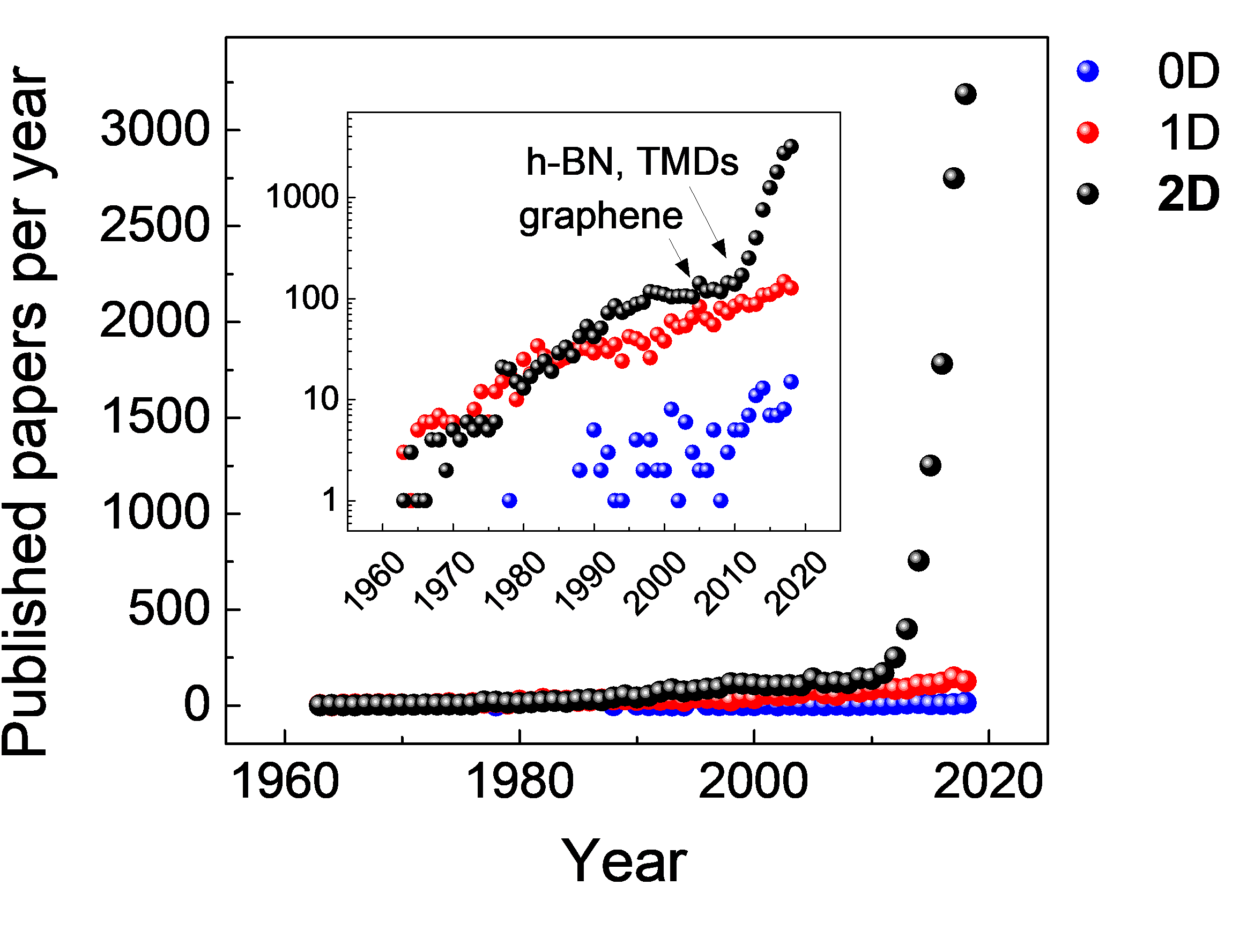
Research in low-dimensional materials has been enjoying extraordinary growth in recent years, increasingly attracting the attention of a multidisciplinary scientific audience both for fundamental science and for technological applications. In particular, the current decade of the 2010s saw the boom of two-dimensional (2D) materials, triggered by pioneering works on graphene in 2004 and subsequent identification, at the beginning of 2010s, of other atomically thin monolayer systems, such as monolayer hexagonal boron nitride (h-BN) and transition metal dichalcogenides (TMDs). Since then, 2D materials and their combination in lateral and vertical heterostructures have been gaining an impressive research interest, accelerated by the availability of an increasingly broad portfolio of 2D candidate materials. The consequent result is the exponential growth in published papers per year, which passed from 139 in 2010 to 3189 in 2018 (see figure below). 2D materials are without doubt one of the most prolific areas of research in the last few years. Due to their thinness, enhanced surface effects, and unprecedented tunable confinement and geometry-related properties, 2D materials constitute a versatile platform for the realization of a new class of functional systems, opening up important applications in very different fields, namely, surface chemistry and (photo)catalysis, DNA nanostructures, biosensors, band–gap engineering, photovoltaics, electronics, photonics, energy storage, harvesting and conversion, nanomedicine, spintronics, and valleytronics. Moreover, van der Waals (vdW) heterostructures have recently emerged as an additional avenue to engineer new properties by stacking 2D compounds in a desired fashion.

text

Number of published research papers per year on zero-, one-, and two-dimensional (0D, 1D, 2D, respectively) materials. For each case, the displayed data are results of Scopus database searches for the eight keywords “**D [or **-dimensional] materials [or compounds, or semiconductors, or crystals]”, where ** = 0 (zero), 1 (one), 2 (two). Milestones in the literature of 2D materials, like the first papers on graphene and those on monolayers of hexagonal boron nitride (h-BN) and transition metal dichalcogenides (TMDs) are indicated in the inset, where results are reported in semi-logarithmic scale. From 2010 to the present, the number of publications per year on 2D materials jumped exponentially from 139 in 2010 to 3189 in 2018.

Given the widespread contemporary interest in 2D materials, crystals, and compounds, the aim of this Special Issue is to provide an up-to-date international platform that can enable scientists from various disciplines to publish the latest advancements and up-to-date reviews on the following topics:

- Novel approaches for preparation of stable and large-scale 2D crystals: bottom–up direct synthesis methods (e.g., chemical vapor deposition, wet–chemical methods, topochemical synthesis), and top–down exfoliation routes (e.g., micromechanical, ultrasonic, ion-exchange exfoliation);

- New efforts put forward to expand the portfolio of 2D materials to search from for optimal properties, encouraging both high-throughput computational methods and experimental research for synthesis of new 2D crystals;

- Lateral and vertical 2D material heterostructures: characterization, fabrication, and study of related devices;

- Characterization techniques of 2D materials: electronic, optical, mechanical properties, morphological analysis (e.g., SEM, TEM), crystallographic studies, and AFM measurements. Particular attention should be given to the study of crystal properties, and to investigating the influence of measurement conditions (e.g., moisture, ambient gas/2D surface interaction, supporting substrate) on the results from characterization techniques;

- Novel applications of 2D materials in pharmacy, biology, medicine, and green chemistry;

- Light–matter interactions in 2D materials, through excitons and polarons;

- Chemical functionalization of 2D materials;

- Ion beam modifications of 2D materials, plasma induced changes to 2D systems, defect engineering;

- Integration of 2D materials with conventional semiconductors for electronics and optoelectronics;

- Theory and modelling of 2D materials and related devices.

Dr. Giuseppe Prestopino
Dr. Giuseppe Arrabito
Guest Editors

Manuscript Submission Information

Manuscripts should be submitted online at www.mdpi.com by registering and logging in to this website. Once you are registered, click here to go to the submission form. Manuscripts can be submitted until the deadline. All submissions that pass pre-check are peer-reviewed. Accepted papers will be published continuously in the journal (as soon as accepted) and will be listed together on the special issue website. Research articles, review articles as well as short communications are invited. For planned papers, a title and short abstract (about 100 words) can be sent to the Editorial Office for announcement on this website.

Submitted manuscripts should not have been published previously, nor be under consideration for publication elsewhere (except conference proceedings papers). All manuscripts are thoroughly refereed through a single-blind peer-review process. A guide for authors and other relevant information for submission of manuscripts is available on the Instructions for Authors page. Crystals is an international peer-reviewed open access monthly journal published by MDPI.

Please visit the Instructions for Authors page before submitting a manuscript. The Article Processing Charge (APC) for publication in this open access journal is 2600 CHF (Swiss Francs). Submitted papers should be well formatted and use good English. Authors may use MDPI's English editing service prior to publication or during author revisions.

Keywords

  • Green chemistry
  • Surface chemistry
  • Growth of 2D crystals: bottom–up and top–down strategies
  • Characterization techniques: electronic transport, optical, and mechanical properties
  • Exfoliation of parent layered compounds
  • Nanoscale engineering
  • van der Waals 2D materials
  • 2D materials
  • Lateral heterostructures
  • Vertical heterostructures
  • Quantum confinement
  • Photophysics of 2D compounds

Published Papers (6 papers)

Order results
Result details
Select all
Export citation of selected articles as:

Research

0 pages, 4167 KiB  
Article
RETRACTED: Artificial Intelligence Algorithm Enabled Industrial-Scale Graphene Characterization
by Wei Sun Leong, Giuseppe Arrabito and Giuseppe Prestopino
Crystals 2020, 10(4), 308; https://doi.org/10.3390/cryst10040308 - 16 Apr 2020
Cited by 12 | Viewed by 4011 | Retraction
Abstract
No characterization method is available to quickly perform quality inspection of 2D materials produced on an industrial scale. This hinders the adoption of 2D materials for product manufacturing in many industries. Here, we report an artificial-intelligence-assisted Raman analysis to quickly probe the quality [...] Read more.
No characterization method is available to quickly perform quality inspection of 2D materials produced on an industrial scale. This hinders the adoption of 2D materials for product manufacturing in many industries. Here, we report an artificial-intelligence-assisted Raman analysis to quickly probe the quality of centimeter-large graphene samples in a non-destructive manner. Chemical vapor deposition of graphene is devised in this work such that two types of samples were obtained: layer-plus-islands and layer-by-layer graphene films, at centimeter scales. Using these samples, we implemented and integrated an unsupervised learning algorithm with an automated Raman spectroscopy to precisely cluster 20,250 and 18,000 Raman spectra collected from layer-plus-islands and layer-by-layer graphene films, respectively, into five and two clusters. Each cluster represents graphene patches with different layer numbers and stacking orders. For instance, the two clusters detected in layer-by-layer graphene films represent monolayer and bilayer graphene based on their Raman fingerprints. Our intelligent Raman analysis is fully automated, with no human operation involved, is highly reliable (99.95% accuracy), and can be generalized to other 2D materials, paving the way towards industrialization of 2D materials for various applications in the future. Full article
(This article belongs to the Special Issue 2D Materials: From Structures to Functions)
Show Figures

Figure 1

11 pages, 10118 KiB  
Article
Electrochemical Characterization of CVD-Grown Graphene for Designing Electrode/Biomolecule Interfaces
by Keishu Miki, Takeshi Watanabe and Shinji Koh
Crystals 2020, 10(4), 241; https://doi.org/10.3390/cryst10040241 - 26 Mar 2020
Cited by 4 | Viewed by 3254
Abstract
In research on enzyme-based biofuel cells, covalent or noncovalent molecular modifications of carbon-based electrode materials are generally used as a method for immobilizing enzymes and/or mediators. However, the influence of these molecular modifications on the electrochemical properties of electrode materials has not been [...] Read more.
In research on enzyme-based biofuel cells, covalent or noncovalent molecular modifications of carbon-based electrode materials are generally used as a method for immobilizing enzymes and/or mediators. However, the influence of these molecular modifications on the electrochemical properties of electrode materials has not been clarified. In this study, we present the electrochemical properties of chemical vapor deposition (CVD)-grown monolayer graphene electrodes before and after molecular modification. The electrochemical properties of graphene electrodes were evaluated by cyclic voltammetry and electrochemical impedance measurements. A covalently modified graphene electrode showed an approximately 25-fold higher charge transfer resistance than before modification. In comparison, the electrochemical properties of a noncovalently modified graphene electrode were not degraded by the modification. Full article
(This article belongs to the Special Issue 2D Materials: From Structures to Functions)
Show Figures

Figure 1

11 pages, 2150 KiB  
Article
Preparation of Few-Layered Wide Bandgap MoS2 with Nanometer Lateral Dimensions by Applying Laser Irradiation
by Mitra Mahdavi, Salimeh Kimiagar and Fahimeh Abrinaei
Crystals 2020, 10(3), 164; https://doi.org/10.3390/cryst10030164 - 2 Mar 2020
Cited by 30 | Viewed by 5089
Abstract
In this study, we report a new method for the quick, green, and one-step preparation of few-layered molybdenum disulfide (MoS2) nanosheets with wide bandgap. MoS2 nanosheets with small lateral dimension and uniform size distribution were synthesized for various applications. MoS [...] Read more.
In this study, we report a new method for the quick, green, and one-step preparation of few-layered molybdenum disulfide (MoS2) nanosheets with wide bandgap. MoS2 nanosheets with small lateral dimension and uniform size distribution were synthesized for various applications. MoS2 powder was synthesized using the hydrothermal method; then, thinned by applying laser irradiation with different energies from 40 to 80 mJ. Transmission electron microscopy (TEM), X-ray diffraction (XRD), Fourier transform infrared spectroscopy (FTIR), UV-Vis absorption spectra, and photoluminescence (PL) spectra were applied for the characterization of the MoS2 nanosheets in terms of morphology, crystal structures, and optical properties. The widest calculated bandgap 4.7 eV was for the sample under 80 mJ laser energy. The results confirmed the successful preparation of highly pure, uniform, and few-layered MoS2 nanosheets. Furthermore, it was possible to enhance the production rate of MoS2 nanosheets (including nanosheets and nanoparticles) through laser irradiation. Thus, the present paper introduces a simple and green alternative approach for preparing few-layered MoS2 nanosheets of transition metal dichalcogenides or other layered materials. Full article
(This article belongs to the Special Issue 2D Materials: From Structures to Functions)
Show Figures

Figure 1

9 pages, 2005 KiB  
Article
The Effect of Ion Irradiation Density on the Defect of Graphene: A Molecular Dynamics Study
by Jinfu Lin, Shulong Wang, Hongxia Liu, Kai Yin, Lei Wu and Wei Li
Crystals 2020, 10(3), 158; https://doi.org/10.3390/cryst10030158 - 1 Mar 2020
Cited by 3 | Viewed by 2599
Abstract
This paper analyzes graphene irradiation effects using a molecular dynamic simulation software, large-scale atomic / molecular massively parallel simulator (LAMMPS). We propose a hypothesis for the effective range of incident ions based on simulation results of irradiation effects that were found using a [...] Read more.
This paper analyzes graphene irradiation effects using a molecular dynamic simulation software, large-scale atomic / molecular massively parallel simulator (LAMMPS). We propose a hypothesis for the effective range of incident ions based on simulation results of irradiation effects that were found using a suspended single-layer graphene. This explains the influence mechanism of irradiation density on the degree of material defects. This paper does key research on how copper substrate influences a single- and bi-layer graphene. The results show that for a single-layer graphene (SLG) the substrate increases the effective range of the incident ions. Within a certain range of the irradiation density, the substrate enhances the defect production on graphene in low-energy irradiation (<5 keV). However, due to the shielding effect of the substrate, the overall trend of graphene damage will be reduced. For the bi-layer graphene (BLG), the effect of the indirect action range is more obvious than that of the direct-action range. In the case of low irradiation density, the knock-on atoms of BLG are much less than suspended SLG. Full article
(This article belongs to the Special Issue 2D Materials: From Structures to Functions)
Show Figures

Figure 1

9 pages, 3521 KiB  
Article
Introducing Electrode Contact by Controlled Micro-Alloying in Few-Layered GaTe Field Effect Transistors
by Xiuxin Xia, Xingdan Sun, Hanwen Wang and Xiaoxi Li
Crystals 2020, 10(3), 144; https://doi.org/10.3390/cryst10030144 - 25 Feb 2020
Cited by 3 | Viewed by 3070
Abstract
Recently, gallium telluride (GaTe) has triggered much attention for its unique properties and offers excellent opportunities for nanoelectronics. Yet it is a challenge to bridge the semiconducting few-layered GaTe crystals with metallic electrodes for device applications. Here, we report a method on fabricating [...] Read more.
Recently, gallium telluride (GaTe) has triggered much attention for its unique properties and offers excellent opportunities for nanoelectronics. Yet it is a challenge to bridge the semiconducting few-layered GaTe crystals with metallic electrodes for device applications. Here, we report a method on fabricating electrode contacts to few-layered GaTe field effect transistors (FETs) by controlled micro-alloying. The devices show linear I-V curves and on/off ratio of ∼10 4 on HfO 2 substrates. Kelvin probe force microscope (KPFM) and energy dispersion spectrum (EDS) are performed to characterize the electrode contacts, suggesting that the lowered Schottky barrier by the diffusion of Pd element into the GaTe conduction channel may play an important role. Our findings provide a strategy for the engineering of electrode contact for future device applications based on 2DLMs. Full article
(This article belongs to the Special Issue 2D Materials: From Structures to Functions)
Show Figures

Figure 1

10 pages, 3589 KiB  
Article
Tunable and Polarization-Independent Plasmon-Induced Transparency in a Fourfold Symmetric Metal-Graphene Terahertz Metamaterial
by Guanqi Wang, Xianbin Zhang, Xuyan Wei and Gaoqi Zhang
Crystals 2019, 9(12), 632; https://doi.org/10.3390/cryst9120632 - 28 Nov 2019
Cited by 4 | Viewed by 2156
Abstract
The introduction of graphene into metamaterials allows for more flexible and convenient control of electromagnetic waves. In this paper, one simple plasmon-induced transparency (PIT) structure with tunability and polarization independence is investigated in the terahertz (THz) regime. The simulation results indicate that the [...] Read more.
The introduction of graphene into metamaterials allows for more flexible and convenient control of electromagnetic waves. In this paper, one simple plasmon-induced transparency (PIT) structure with tunability and polarization independence is investigated in the terahertz (THz) regime. The simulation results indicate that the transparent window can be manipulated in a wide range and even switched off by merely changing the Fermi energy of graphene. By continuously altering the resonance intensity of the dark resonator using the graphene, the PIT resonance can be actively manipulated. The behavior can be elucidated by the classical coupled two-particle model, which corresponds well to the simulation results. Owing to the fourfold symmetric structure, the proposed PIT device exhibits polarization-independent characteristics. This work provides design guidance for metal-graphene THz modulators. Full article
(This article belongs to the Special Issue 2D Materials: From Structures to Functions)
Show Figures

Figure 1

Back to TopTop