Article

Electronic Structure of C60/Zinc Phthalocyanine/V2O5 Interfaces Studied Using Photoemission Spectroscopy for Organic Photovoltaic Applications

1
Department of Physics, Yonsei University, 1 Yonseidae-gil, Wonju-si, Gangwon-do 26493, Korea
2
Institute of Physics and Applied Physics, Yonsei University, 50 Yonsei-ro, Seodaemun-Gu, Seoul 03722, Korea
3
Department of Physics, Kangwon National University, 1 Gangwondaehak-gil, Chuncheon-si, Gaongwon-do 24341, Korea
*
Author to whom correspondence should be addressed.
Molecules 2018, 23(2), 449; https://doi.org/10.3390/molecules23020449
Submission received: 13 January 2018 / Revised: 11 February 2018 / Accepted: 14 February 2018 / Published: 18 February 2018
(This article belongs to the Special Issue Advanced Functional Dyes)

Abstract

:
The interfacial electronic structures of a bilayer of fullerene (C60) and zinc phthalocyanine (ZnPc) grown on vanadium pentoxide (V2O5) thin films deposited using radio frequency sputtering under various conditions were studied using X-ray and ultraviolet photoelectron spectroscopy. The energy difference between the highest occupied molecular orbital (HOMO) level of the ZnPc layer and the lowest unoccupied molecular orbital (LUMO) level of the C60 layer was determined and compared with that grown on an indium tin oxide (ITO) substrate. The energy difference of a heterojunction on all V2O5 was found to be 1.3~1.4 eV, while that on ITO was 1.1 eV. This difference could be due to the higher binding energy of the HOMO of ZnPc on V2O5 than that on ITO regardless of work functions of the substrates. We also determined the complete energy level diagrams of C60/ZnPc on V2O5 and ITO.

Graphical Abstract

1. Introduction

Organic photovoltaics (OPVs) have received increasing attention over the past few years due to their potential as a renewable, cheap, and economical source of power [1,2,3,4,5,6]. However, despite significant recent advances in their cell performance, the current power conversion efficiencies remain too low for commercial viability of such cells. A general problem of organic electronic devices is the poor transport of charge carriers at the interface between electrodes and the organic semiconductor. Consequently, recent efforts have been made to improve charge transport and collection at the electrodes. In particular, the use of transition metal oxides as a transparent electrode has attracted considerable interest [7]. Indium tin oxide (ITO) is widely used as an electrode in OPV fabrication and as a transparent conducting electrode for light-emitting diodes due to its reasonable transparency in the visible region, good conductivity, and ease of patterning. However, the surface chemistry of ITO is difficult to control [8] and ITO has become approximately 10 times more expensive over the past few years due to diminishing indium resources [9]. In fact, the cost of indium is expected to increase because of the increasing demand from producers of solar cells in addition to the demand from the existing flat-panel display industry [10]. Transition metal oxides are believed to prevent unwanted chemical reactions between transparent electrodes and an optically active organic layer [11,12,13]. Furthermore, a high work function material such as a metal oxide is desirable to decrease the series resistance in devices [14]. Due to different oxidation states, vanadium can be used to create many compounds with oxygen such as vanadium monoxide (VO), vanadium sesquioxide (V2O3), vanadium dioxide (VO2), vanadium pentoxide (V2O5), V3O7, V6O13, and V4O9 [15], which exhibit specific properties depending on structure. At a critical temperature, crystallographic transformation shows that vanadium oxide accompanies a reversible semiconductor-to-metal transition that alters its optical and electrical properties [16]. Among the possible compounds of vanadium oxides, the stable V2O5 phase possesses a wide optical band gap, good chemical and thermal stability, and excellent thermoelectric properties, which suggest that V2O5 is a potential candidate in several applications including electro-chromic displays, gas sensing, and optoelectronic devices [17,18,19,20]. Different deposition techniques such as spray pyrolysis, ultrasonic spray pyrolysis, spin coating, thermal evaporation, electron beam evaporation, radio frequency sputtering, dc magnetron sputtering, sol-gel, and chemical vapor deposition have been used to deposit vanadium oxide thin films in order to improve the optical and electrical properties of transparent conductive oxides (TCOs).
In this study, the electronic structures and energy level alignment of a bilayer of C60 and ZnPc grown on V2O5 thin films deposited using radio frequency sputtering under various conditions were studied. The electronic structure was measured using in-situ ultraviolet photoemission spectroscopy (UPS) and X-ray photoemission spectroscopy (XPS). The separation of the highest occupied molecular orbital (HOMO) of the donor and the lowest unoccupied molecular orbital (LUMO) of the acceptor (EDHOMO–EALUMO) was measured for each bilayer because EDHOMO–EALUMO is a strong factor in determining the magnitude of the measured open circuit voltage (VOC) of an OPV cell based on a donor–acceptor heterojunction [21,22].

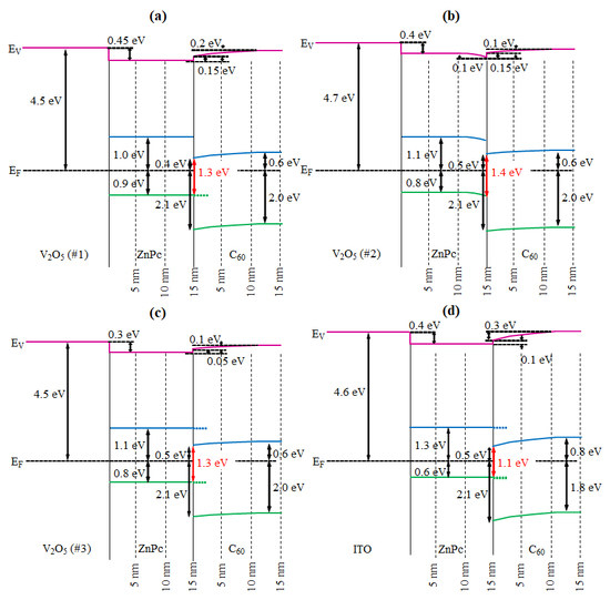
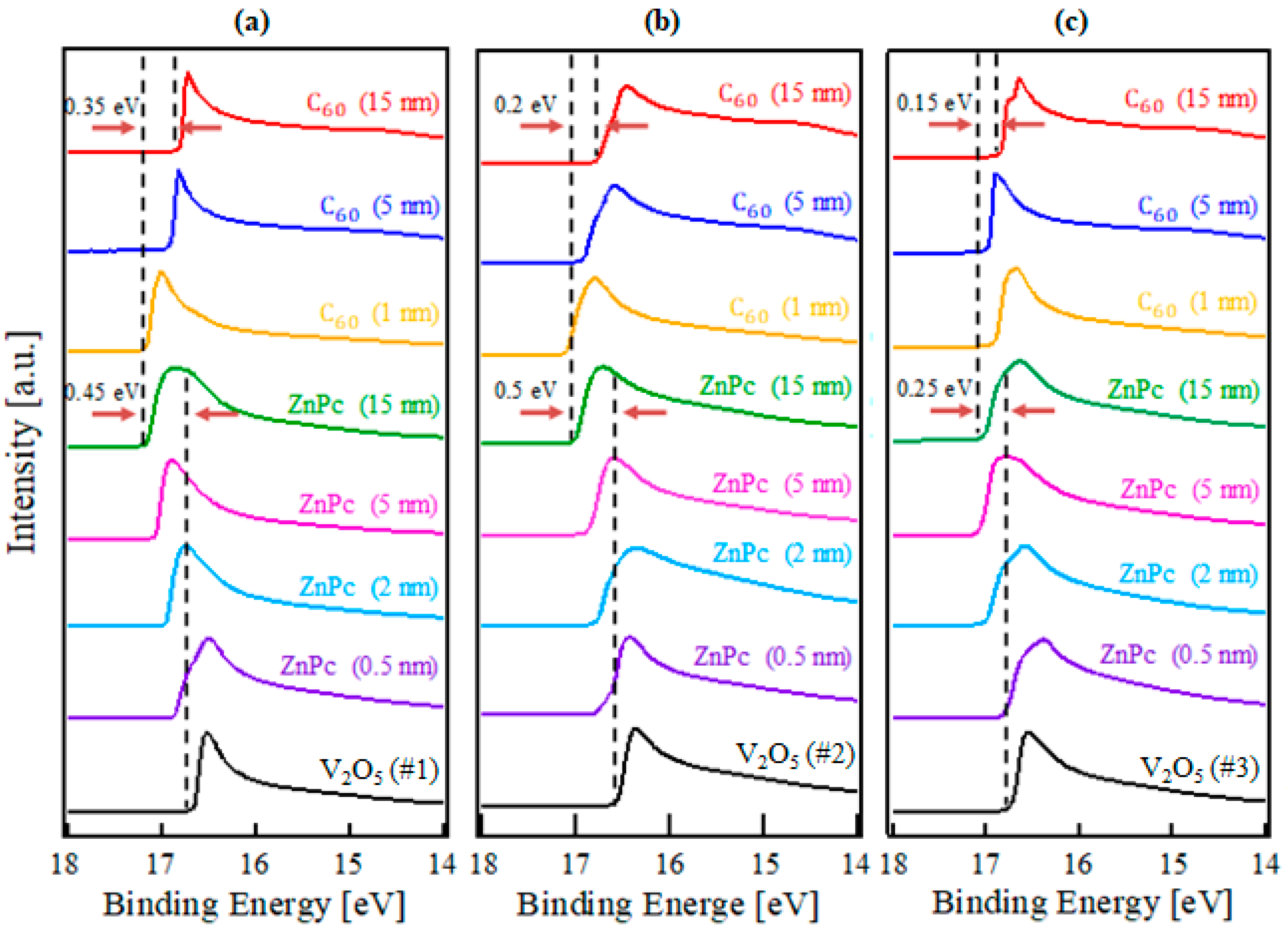
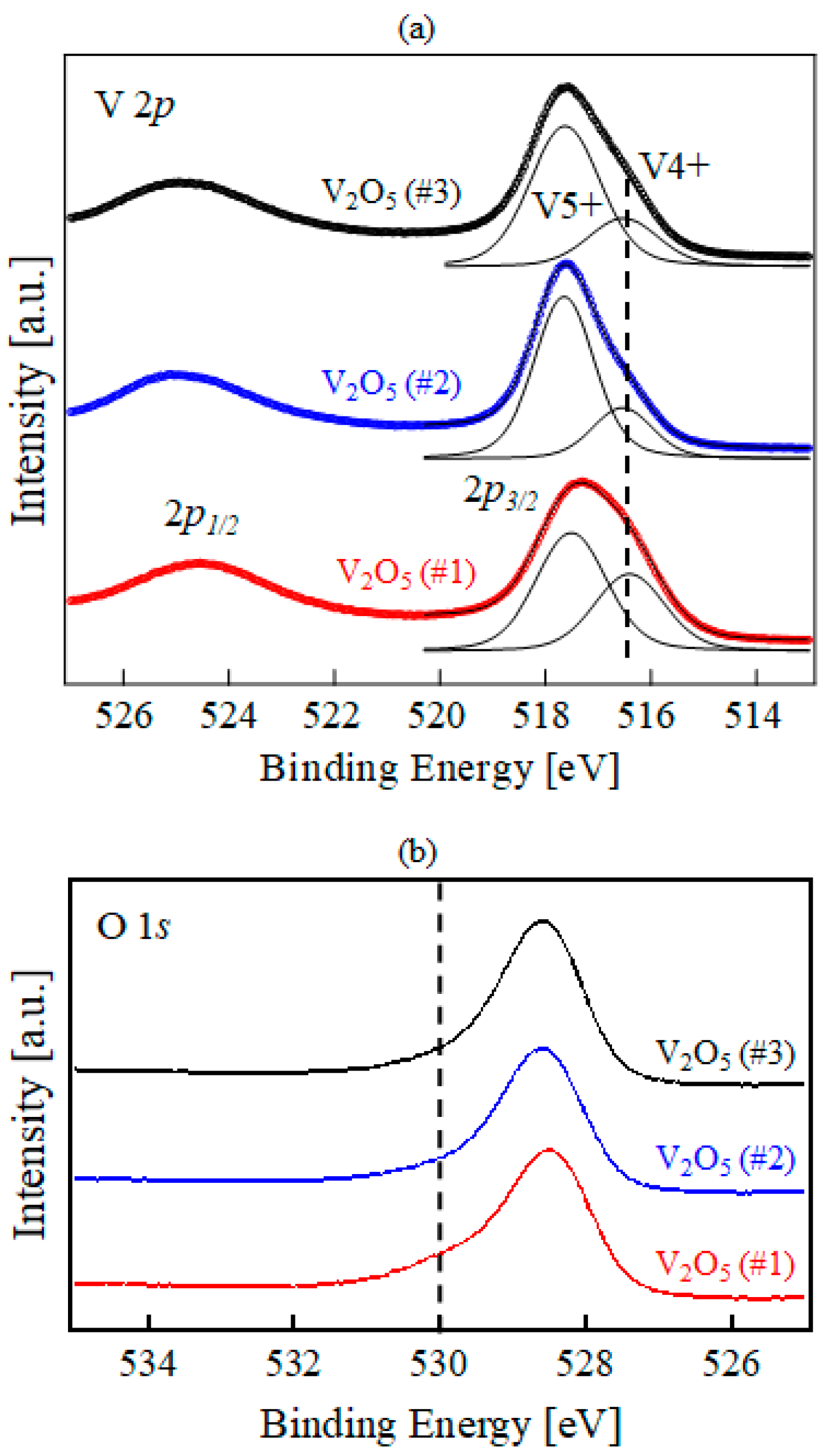
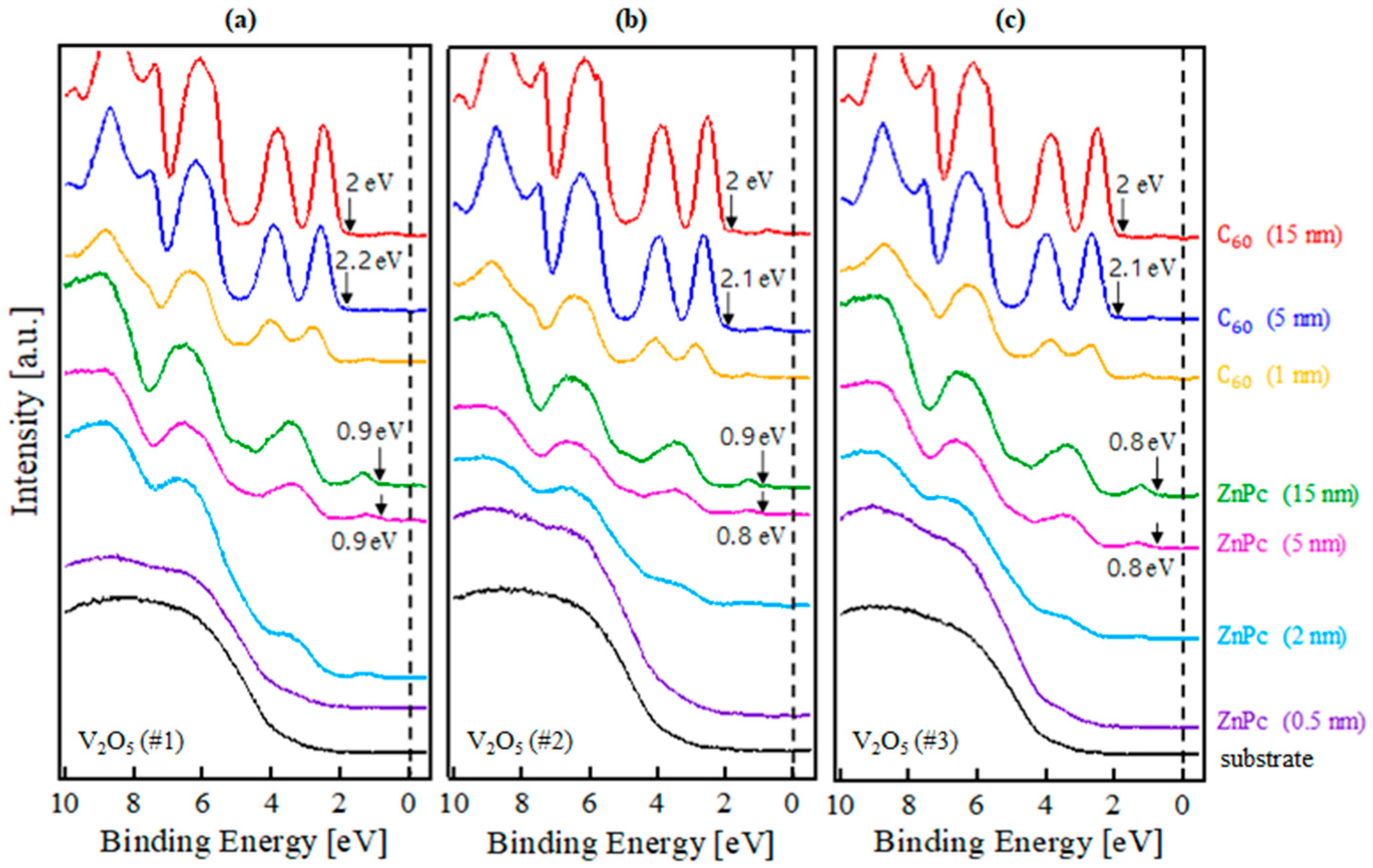
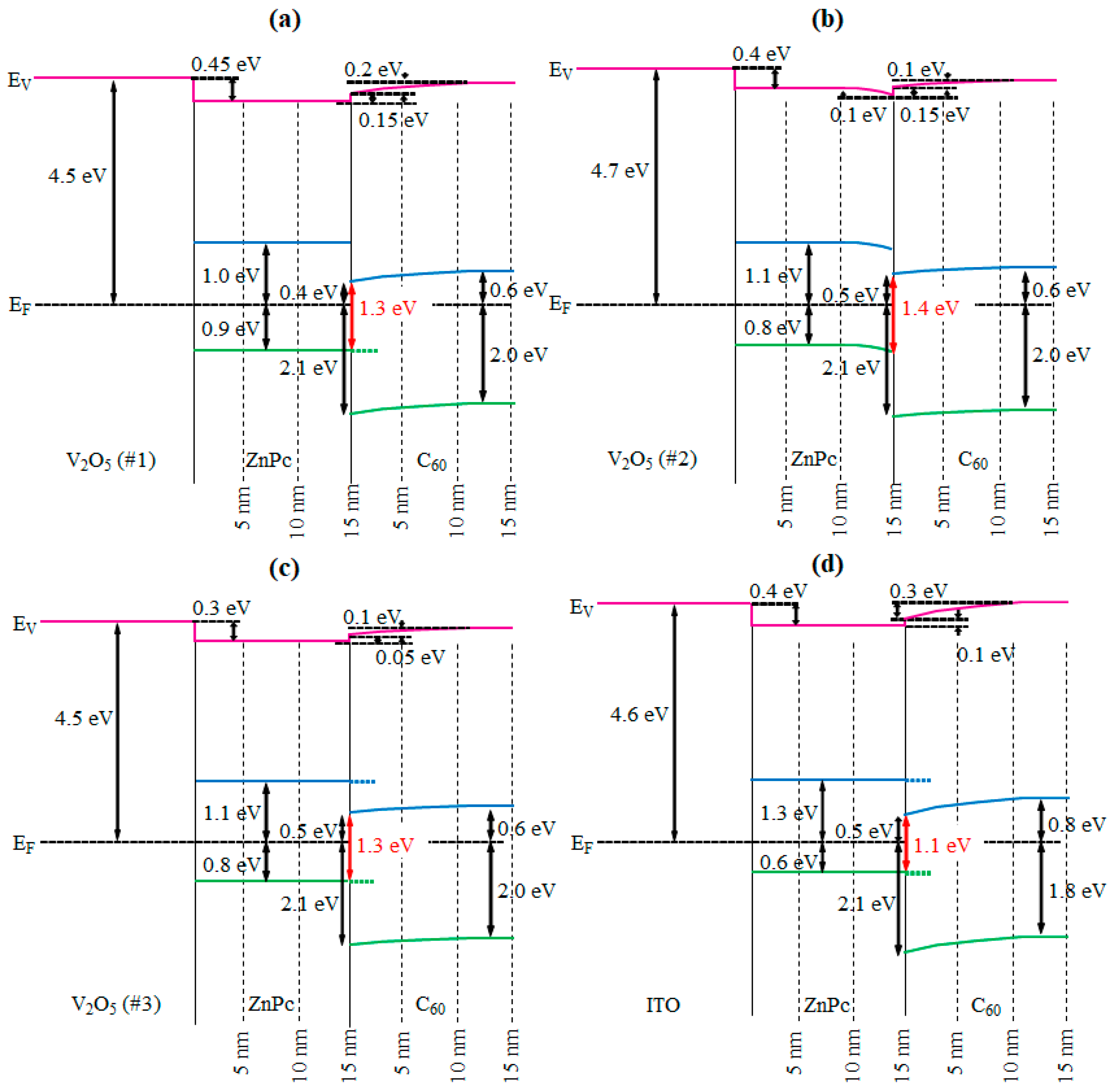
2. Results and Discussion

As shown in Table 1, V2O5 samples were fabricated under three different growth conditions. The V2O5 #1 sample was grown in an Ar atmosphere for 5 min, and the V2O5 #2 sample was grown in an Ar atmosphere for 20 min. Alternatively, the V2O5 #3 sample was deposited in an Ar:O2 atmosphere (at a ratio of 29:1) for 20 min. The sheet resistances of the samples were not significantly different.
To determine the chemical state of the elements in the obtained samples, XPS analysis was carried out. These results are shown in Figure 1. For vanadium, a complex energy distribution of V 2p photoelectrons was obtained. The V 2p core level spectrum is dominated by a spin-orbit doublet with peaks at binding energies of about 517.5 and 525.0 eV. Both the binding energy and spin-orbit splitting are in good agreement with values previously reported for V2O5 [23]. The line shapes of these spectra were analyzed by a standard least squares fitting scheme using a convolution of Gaussian and Lorentzian peaks. The width of the Lorentzian peaks was assumed to be the same for each component. We obtain an fwhm for the Lorentzian of about 0.35 eV for V 2p3/2. The FWHM for the Gaussian resulting from the fitting procedure is 1.20~1.40 eV. As shown in Figure 1a, an additional peak in the V 2p3/2 core level was also observed at lower binding energy (about 516.4 eV) in all samples; however, the relative intensity of that in V2O5 #1 was greater than in the others. The peak position is close to that reported for single crystalline VO2 [23]. The oxidation states of vanadium V2O5 and VO2 are V5+ and V4+, respectively. This means that the V2O5 #1 sample did not have enough deposition time to form a perfect composition and had relatively more oxygen vacancies, which account for the higher defect level and greater abundance of trap-assisted conducting oxides than in the others. In Figure 1b, an additional O 1s core level was also observed at higher binding energies in all samples. The relative intensity of that of V2O5 #1 is also greater than the others in the O 1s core level spectra.
The electronic structures during the interface formation of C60/ZnPc/V2O5 #1, #2, and #3 were investigated using in-situ UPS. Figure 2 and Figure 3 show UPS spectra obtained for the deposition of C60/ZnPc on various V2O5 thin films. The spectra shown in Figure 2a–c were collected in the secondary electron cut-off region for the V2O5 #1, V2O5 #2, and V2O5 #3 layers, respectively. The supplementary material (Figure S1) illustrates the procedure used for the determination of energy-level alignment at the interface. The secondary cut-off position moved noticeably toward a higher binding energy as soon as the ZnPc deposition began on each substrate. The shift of the secondary cut-off position is attributed to the formation of an interface dipole and band bending [24,25]. However, the secondary cut-off position moved toward lower binding energies as soon as C60 deposition began on each ZnPc layer. In these spectra, the total shift of the cut-off position of ZnPc toward higher binding energies was 0.45, 0.50, and 0.25 eV, while that of C60 on the ZnPc layer was 0.35, 0.20, and 0.15 eV toward lower binding energies for V2O5 #1, V2O5 #2, and V2O5 #3, respectively.
Figure 3a–c show the evolution of HOMO onset during the growth of the C60/ZnPc layer on V2O5 #1, V2O5 #2, and V2O5 #3, respectively. As shown in Figure 3a, there was no shift in HOMO onset of ZnPc for the ZnPc/V2O5 #1 interface and the HOMO onset was measured at 0.9 eV below the Fermi level. It is clear that the HOMO of C60 gradually shifted toward lower binding energies, and total shift reached 0.2 eV after the shifts were saturated. This result confirms that band bending occurred at the C60/ZnPc interface. The saturated HOMO onset of the C60 layer was 2.0 eV below the Fermi level. In Figure 3b, the HOMO onset of ZnPc gradually shifted toward higher binding energies from 0.8 to 0.9 eV, confirming band bending at the ZnPc/V2O5 #2 interface. It was also observed that the HOMO of C60 gradually shifted toward lower binding energies, and the total shift reached 0.1 eV. The saturated HOMO onset of the C60 layer was 2.0 eV below the Fermi level. In Figure 3c, the HOMO onset of ZnPc on V2O5 #3 did not shift, and the HOMO onset was measured at 0.8 eV below the Fermi level. The HOMO of C60 shifted toward lower binding energies from 2.1 to 2.0 eV.
An energy level diagram was constructed by combining the changes of the spectra shown in Figure 2 and Figure 3. We estimate that the overall measurement errors in orbital offsets and interface dipoles are of the order of ±0.05 eV. We determined the energy positions according to the systematic procedure as described in detail in [7]. Additionally, the energy level diagram of C60/ZnPc/ITO based on our data (not shown here) is displayed. As shown in Figure 4, the energy gaps between the HOMO and LUMO of ZnPc and C60 were about 1.9 and 2.6 eV, respectively, as previously reported [26,27]. The measured work functions of V2O5 #1, V2O5 #2, and V2O5 #3 were estimated to be about 4.5, 4.7, and 4.5 eV, respectively. The energy level difference between the HOMO of the donor (ZnPc) and the LUMO of the acceptor (C60), EDHOMO–EALUMO is an important factor in determining the magnitude of VOC of OPVs based on a donor–acceptor heterojunction. However, a correction term between the real VOC and the EDHOMO–EALUMO value may be required to account for voltage losses in the device due to large diode quality factors, high reverse saturation currents, low-field-dependent mobilities of charge carriers, and voltage losses at the collection electrodes.
The C60/ZnPc heterojunction on V2O5 #2 showed the largest EDHOMO–EALUMO value (1.4 eV). The measured EDHOMO–EALUMO values on V2O5 #1 and V2O5 #3 were the same (1.3 eV). There are several factors that can affect the magnitude of EDHOMO–EALUMO at the donor–acceptor interface, including the ionization potential of a donor, the electron affinity of an acceptor, the formation of interface dipoles, and charge redistribution across the interfaces. In this case, the band bending of ZnPc was observed only at the ZnPc/V2O5 #2 interface, and the band bending moved the HOMO of the donor (ZnPc) toward higher binding energies and increased the EDHOMO–EALUMO value. In general, this is due to different degrees of charge transfer from the substrate to the ZnPc layer, and the work function difference of substrates is the origin of the different degrees of charge transfer. However, the value of band bending (0.1 eV) was almost negligible considering the measurement error. Therefore, this 0.1 eV difference of the EDHOMO–EALUMO value was not predicted to lead to enhanced values of VOC for OPVs. On the other hand, the measured EDHOMO–EALUMO values on ITO was 1.1 eV, which is smaller than those on V2O3 samples. This means that the OPV using V2O3 as an anode should have a larger VOC than that using ITO. This is because the HOMO onset of ZnPc on ITO was 0.2~0.3 eV lower than that on the V2O5 regardless of work functions of the substrates. To understand the underlying cause, further studies should be conducted comparing the charge neutrality level of ZnPc with the density of states of V2O5 and ITO. Therefore, not only the work functions of new TCOs but also the charge neutrality level of donors should be considered for controlling the VOC for high-efficiency OPVs.

3. Methods

V2O5 films on ITO substrate were prepared by radio frequency magnetron sputtering of V2O5 targets at room temperature. Before deposition the ITO substrates were sequentially cleaned ultrasonically in acetone, alcohol, and de-ionized water before finally being dried in nitrogen gas. The distance between the target and substrate was approximately 100 mm. The radio frequency magnetron working power was 200 W, and deposition times were 5 and 20 min. The base pressure was 5.7 × 10⁻⁷ Torr and the working pressure was 2.5 m Torr. As shown in Table 1, three V2O5 films at different deposition times and flowing gas compositions were prepared.
The chemical states for the V2O5 films grown on ITO were examined by XPS. XPS core level spectra of V 2p and O 1s were obtained using a monochromatic Al Ka X-ray source. In situ UPS measurements were carried out using a PHOIBOS 150 energy analyzer (SPECS GmbH, Berlin, Germany) and an ultraviolet (He I, 21.22 eV) light source. The base pressure of the analysis chamber was 5 × 10⁻¹⁰ Torr. ZnPc and C60 were thermally evaporated on V2O5 and ITO substrates at a rate of 0.01 nm/s. The total thickness and deposition rate were monitored by a quartz crystal microbalance. The secondary electron cut-off (SEC) positions were measured in normal emission geometry with a sample bias of −5 V.

4. Conclusions

The interfacial electronic structures of a bilayer of C60 and ZnPc grown on V2O5 thin films deposited using radio frequency sputtering under various conditions were studied using X-ray and ultraviolet photoelectron spectroscopy. The energy difference between the HOMO level of the ZnPc layer and the LUMO level of the C60 layer was determined and compared with that grown on ITO substrate. The energy difference of a heterojunction on all V2O5 was found to be 1.3~1.4 eV, while that on ITO was 1.1 eV. This difference could be due to the HOMO of ZnPc on V2O5 having a higher binding energy than that on ITO regardless of work functions of the substrates. We also determined the complete energy level diagrams of C60/ZnPc on V2O5 and ITO.

Supplementary Materials

The Supplementary Materials are available online.

Acknowledgments

This research was supported by the Basic Science Research Programs through the National Research Foundation of Korea (Grant No. NRF-2017R1D1A3B03034867) and Yonsei University Wonju Campus Future-leading Research Initiative (Grant No. 2017-52-0071)

Author Contributions

C.J.L. and S.W.C. designed the experiment. C.J.L., M.G.P., M.S.K., and J.H.H. performed the experiments and analyzed the data. C.J.L. and S.W.C. wrote the main manuscript text. S.C. Y.Y., M.-H.C., and H.L. participated in discussion through the work.

Conflicts of Interest

The authors declare no conflict of interest.

References

  1. Peng, Y.; Yaacobi-Gross, N.; Perumal, A.K.; Faber, H.A.; Vourlias, G.; Patsalas, P.A.; Bradley, D.D.C.; He, Z.Q.; Anthopoulos, T.D. Efficient organic solar cells using copper(I) iodide (CuI) hole transport layers. Appl. Phys. Lett. 2015, 106. [Google Scholar] [CrossRef]
  2. Falke, S.M.; Rozzi, C.A.; Brida, D.; Maiuri, M.; Amato, M.; Sommer, E.; De Sio, A.; Rubio, A.; Cerullo, G.; Molinari, E.; et al. Coherent ultrafast charge transfer in an organic photovoltaic blend. Science 2014, 344, 1001–1005. [Google Scholar] [CrossRef] [PubMed] [Green Version]
  3. Sullivan, P.; Duraud, A.; Hancox, I.; Beaumont, N.; Mirri, G.; Tucker, J.H.R.; Hatton, R.A.; Shipman, M.; Jones, T.S. Halogenated boron subphthalocyanines as light harvesting electron acceptors in organic photovoltaics. Adv. Energy Mater. 2011, 1, 352–355. [Google Scholar] [CrossRef]
  4. Silvestri, F.; Marrocchi, A.; Seri, M.; Kim, C.; Marks, T.J.; Facchetti, A.; Taticchi, A. Solution-processable low-molecular weight extended arylacetylenes: Versatile p-Type semiconductors for field-effect transistors and bulk heterojunction solar cells. J. Am. Chem. Soc. 2010, 132, 6108–6123. [Google Scholar] [CrossRef] [PubMed]
  5. Brabec, C.J. Organic photovoltaics: Technology and market. Sol. Energy Mater. Sol. C 2004, 83, 273–292. [Google Scholar] [CrossRef]
  6. Garcias-Morales, C.; Romero-Borja, D.; Maldonado, J.-L.; Roa, A.; Rodríguez, M.; García-Merinos, J.; Ariza-Castolo, A. Small molecules derived from Thieno[3,4-c]pyrrole-4,6-dione (TPD) and their use in solution processed organic solar cells. Molecules 2017, 22. [Google Scholar] [CrossRef] [PubMed]
  7. Lee, H.; Cho, S.W.; Yi, Y. Interfacial electronic structure for high performance organic devices. Curr. Appl. Phys. 2016, 16, 1533–1549. [Google Scholar] [CrossRef]
  8. Kim, J.S.; Friend, R.H.; Grizzi, I.; Burroughes, J.H. Spin-cast thin semiconducting polymer interlayer for improving device efficiency of polymer light-emitting diodes. Appl. Phys. Lett. 2005, 87. [Google Scholar] [CrossRef]
  9. Bhosle, V.; Prater, J.T.; Yang, F.; Burk, D.; Forrest, S.R.; Narayan, J. Gallium-doped zinc oxide films as transparent electrodes for organic solar cell applications. J. Appl. Phys. 2007, 102. [Google Scholar] [CrossRef]
  10. Murdoch, G.B.; Hinds, S.; Sargent, E.H.; Tsang, S.W.; Mordoukhovski, L.; Lu, Z.H. Aluminum doped zinc oxide for organic photovoltaics. Appl. Phys. Lett. 2009, 94. [Google Scholar] [CrossRef]
  11. Shrotriya, V.; Li, G.; Yao, Y.; Chu, C.W.; Yang, Y. Transition metal oxides as the buffer layer for polymer photovoltaic cells. Appl. Phys. Lett. 2006, 88. [Google Scholar] [CrossRef]
  12. Zou, J.Y.; Li, C.Z.; Chang, C.Y.; Yip, H.L.; Jen, A.K.Y. Interfacial engineering of ultrathin metal film transparent electrode for flexible organic photovoltaic cells. Adv. Mater. 2014, 26, 3618–3623. [Google Scholar] [CrossRef] [PubMed]
  13. Heo, N.; Kim, Y.; Jung, Y.; Cheon, S.; Cho, S.; Cho, S.W.; Park, S.; Yi, Y.; Smith, K.E. Interfacial electronic structure of C-60/ZnPc/AZO on photoemission spectroscopy for organic photovoltaic applications. Chem. Phys. 2016, 478, 145–149. [Google Scholar] [CrossRef]
  14. Cattin, L.; Dahou, F.; Lare, Y.; Morsli, M.; Tricot, R.; Houari, S.; Mokrani, A.; Jondo, K.; Khelil, A.; Napo, K.; et al. MoO3 surface passivation of the transparent anode in organic solar cells using ultrathin films. J. Appl. Phys. 2009, 105. [Google Scholar] [CrossRef]
  15. Beke, S. A review of the growth of V2O5 films from 1885 to 2010. Thin Solid Films 2011, 519, 1761–1771. [Google Scholar] [CrossRef]
  16. Morin, F.J. Oxides which show a metal-to-insulator transition at the neel temperature. Phys. Rev. Lett. 1959, 3, 34–36. [Google Scholar] [CrossRef]
  17. Iida, Y.; Kaneko, Y.; Kanno, Y. Fabrication of pulsed-laser deposited V2O5 thin films for electrochromic devices. J. Mater. Process. Technol. 2008, 197, 261–267. [Google Scholar] [CrossRef]
  18. Luo, Z.; Wu, Z.; Xu, X.; Du, M.; Wang, T.; Jiang, Y. Impact of substrate temperature on the microstructure, electrical and optical properties of sputtered nanoparticle V2O5 thin films. Vacuum 2010, 85, 145–150. [Google Scholar] [CrossRef]
  19. Mousavi, M.; Kompany, A.; Shahtahmasebi, N.; Bagheri-Mohagheghi, M.M. Effect of S-doping on structural, optical and electrochemical properties of vanadium oxide thin films prepared by spray pyrolysis. Phys. Scr. 2013, 88. [Google Scholar] [CrossRef]
  20. Mousavi, M.; Kompany, A.; Shahtahmasebi, N.; Bagheri-Mohagheghi, M.M. Study of structural, electrical and optical properties of vanadium oxide condensed films deposited by spray pyrolysis technique. Adv. Manuf. 2013, 1, 320–328. [Google Scholar] [CrossRef]
  21. Piper, L.F.J.; Cho, S.W.; Zhang, Y.; DeMasi, A.; Smith, K.E.; Matsuura, A.Y.; McGuinness, C. Soft X-ray spectroscopy study of the element and orbital contributions to the electronic structure of copper hexadecafluoro-phthalocyanine. Phys. Rev. B 2010, 81, 1–12. [Google Scholar] [CrossRef]
  22. Chauhan, V.; Hatton, R.; Sullivan, P.; Jones, T.; Cho, S.W.; Piper, L.; deMasi, A.; Smith, K. Elucidating the factors that determine the open circuit voltage in discrete heterojunction organic photovoltaic cells. J. Mater. Chem. 2010, 20, 1173–1178. [Google Scholar] [CrossRef]
  23. Demeter, M.; Neumann, M.; Reichelt, W. Mixed-valence vanadium oxides studied by XPS. Surf. Sci. 2000, 454–456, 41–44. [Google Scholar] [CrossRef]
  24. Lee, S.T.; Hou, X.Y.; Mason, M.G.; Tang, C.W. Energy level alignment at Alq/metal interfaces. Appl. Phys. Lett. 1998, 72, 1593–1595. [Google Scholar] [CrossRef]
  25. Ishii, H.; Sugiyama, K.; Ito, E.; Seki, K. Energy level alignment and interfacial electronic structures at organic metal and organic organic interfaces. Adv. Mater. 1999, 11, 605–625. [Google Scholar] [CrossRef]
  26. Gao, W.Y.; Kahn, A. Electronic structure and current injection in zinc phthalocyanine doped with tetrafluorotetracyanoquinodimethane: Interface versus bulk effects. Org. Electron. 2002, 3, 53–63. [Google Scholar] [CrossRef]
  27. Mitsumoto, R.; Seki, K.; Araki, T.; Ito, E.; Ouchi, Y.; Achiba, Y.; Kikuchi, K.; Yajima, S.; Kawasaki, S.; Okino, F.; et al. Soft X-ray absorption, UV photoemission, and VUV absorption spectroscopic studies of fluorinated fullerenes. J. Electron. Spectrosc. Relat. Phenom. 1996, 78, 453–456. [Google Scholar] [CrossRef]
Sample Availability: Samples of the compounds are not available from the authors.
Figure 1. (a) V 2p and (b) O 1s core level photoemission spectra of V2O5 #1, V2O5 #2, and V2O5 #3, measured with a monochromatic Al Ka X-ray source.
Molecules 23 00449 g001
Figure 2. The UPS spectra in the secondary cut-off region collected during the step-by-step layer deposition of C60/ZnPc on (a) V2O5 #1, (b) V2O5 #2, and (c) V2O5 #3 surfaces.
Molecules 23 00449 g002
Figure 3. The UPS spectra collected near the Fermi level as a function of the C60/ZnPc deposition thickness on (a) V2O5 #1, (b) V2O5 #2, and (c) V2O5 #3 surfaces.
Molecules 23 00449 g003
Figure 4. Energy level diagrams of C60/ZnPc on (a) V2O5 #1, (b) V2O5 #2, (c) V2O5 #3, and (d) ITO surfaces.
Molecules 23 00449 g004
Table 1. The growth conditions of V2O5 #1, #2, and #3.
V2O5 #1
Growth time (min)5
Gas flow (sccm)Ar = 30
Sheet resistivity (Ω/sq.)48
V2O5 #2
Growth time (min)20
Gas flow (sccm)Ar = 30
Sheet resistivity (Ω/sq.)46
V2O5 #3
Growth time (min)20
Gas flow (sccm)Ar:O2 = 29:1
Sheet resistivity (Ω/sq.)36

