A Reduced Three Dimensional Model for SAW Sensors Using Finite Element Analysis

Abstract
:1. Introduction
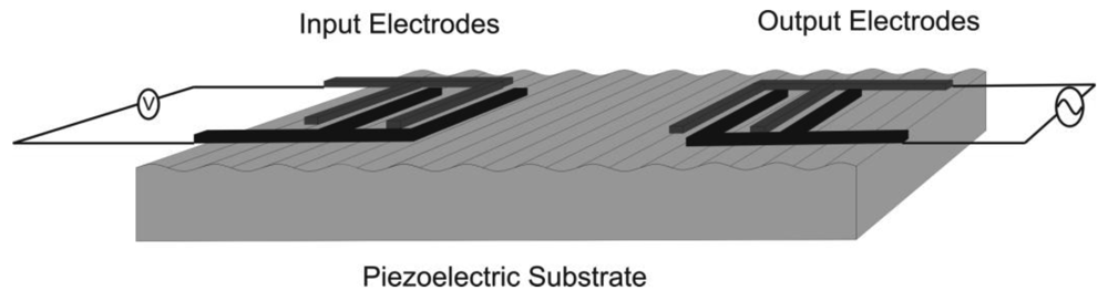
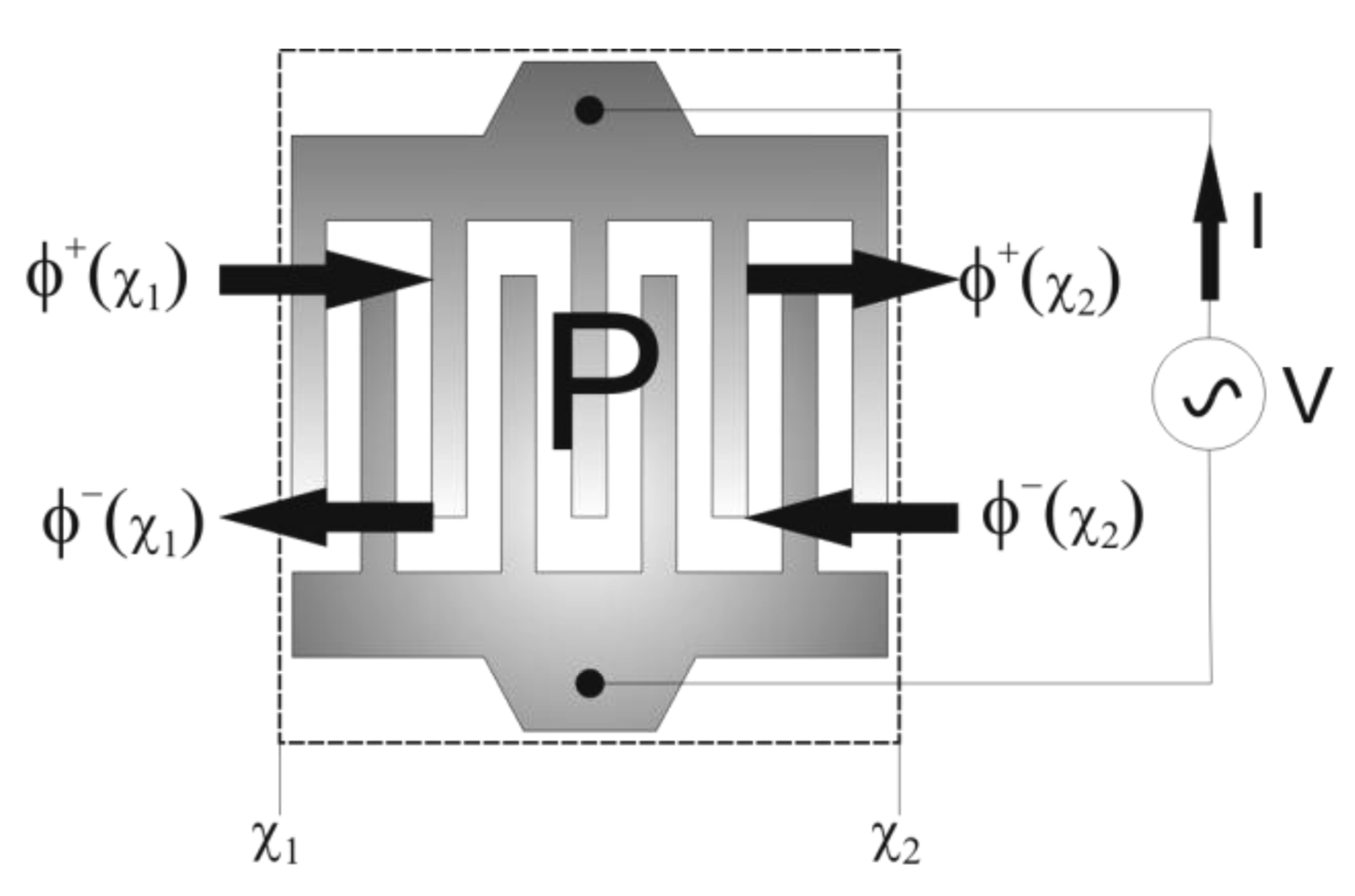
2. Operating Principle of SAW Devices
2.1. Plane Wave Solution
2.2. Frequency Response of SAW Devices
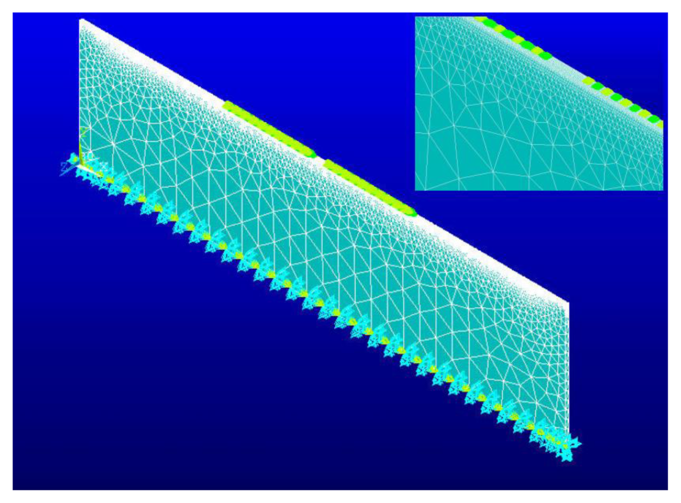
3. Numerical Model of the SAW Sensor Using the Finite Element Method
| Mass Matrix [M] | |
| Mechanical Stiffness Matrix [Kuu] | |
| Mechanical Body Force Matrix [FB] | |
| Mechanical Surface Force Matrix [FS] | |
| Mechanical Point Force Matrix [FP] | |
| Mechanical Damping Matrix [Duu] | |
| Piezoelectric Coupling Matrix [Kuφ] | |
| Dielectric Stiffness Matrix [Kφφ] | |
| Electrical Surface Charge Matrix [Qs] | |
| Electrical Point Charge Matrix [QP] | |
| *α and β are Damping coefficients | |
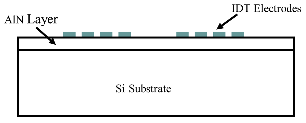
4. Reduced 3D Model (R3D) of Aluminum Nitride-Silicon (AlN/Si(111)) SAW Sensor
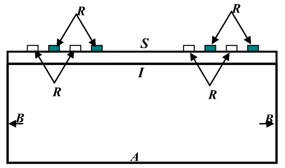
Boundary Conditions
- Clamped condition on the bottom surface A, to fix the sensor in place and reduce second order effects [7]:
- Continuity of the displacement field components Ui for i = x, y, z at interface I.
- A Traction free boundary at the free surface S (z-plane):
- The following Dirichlet conditions for the electric potential:where V(t) is the input voltage signal and O(t) is the voltage response at the output electrodes.
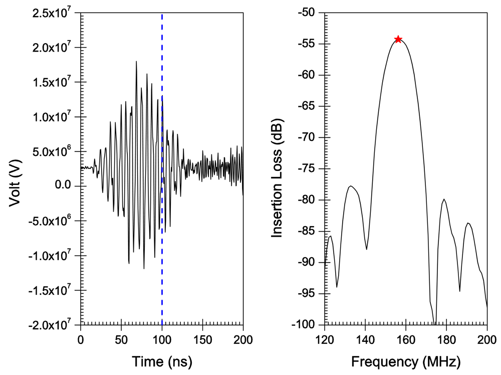
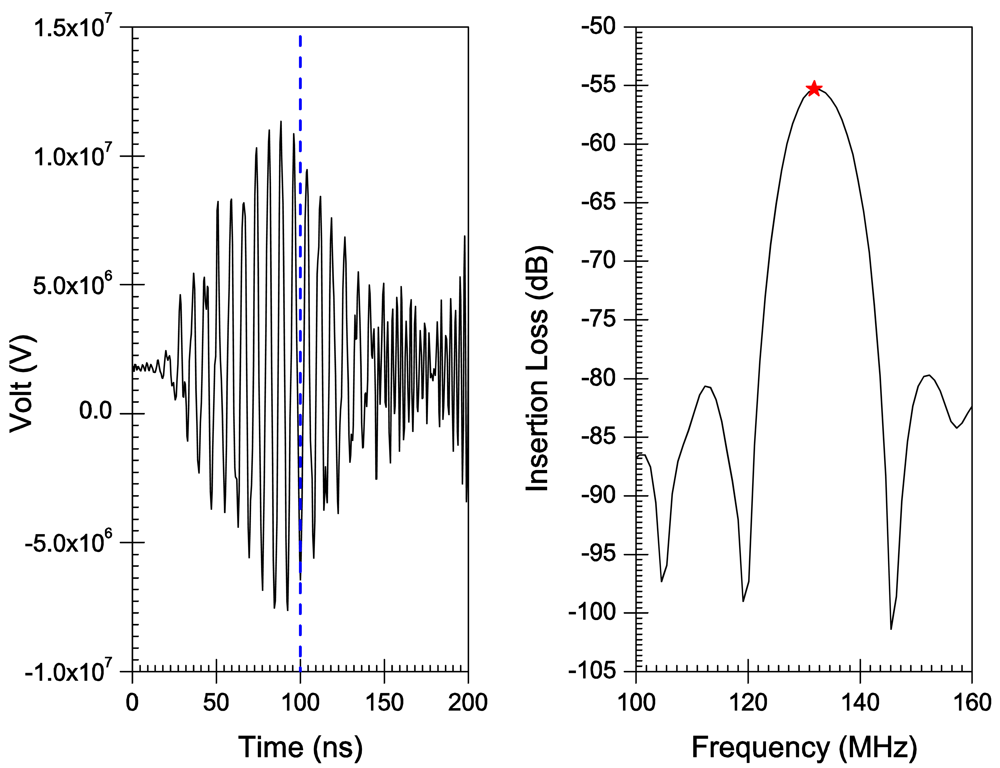
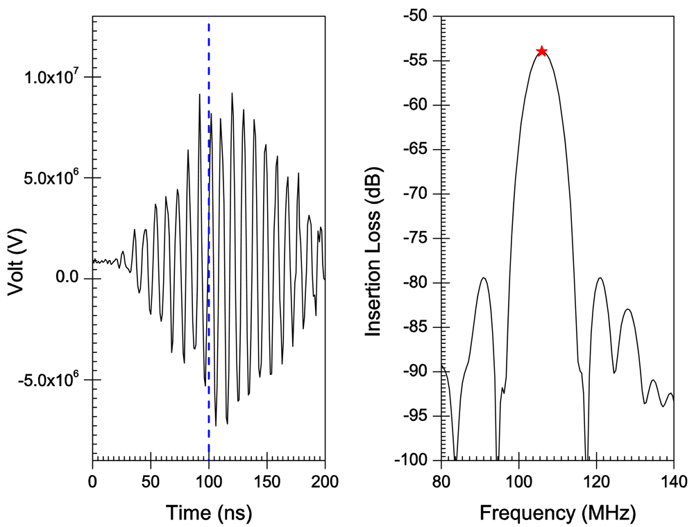
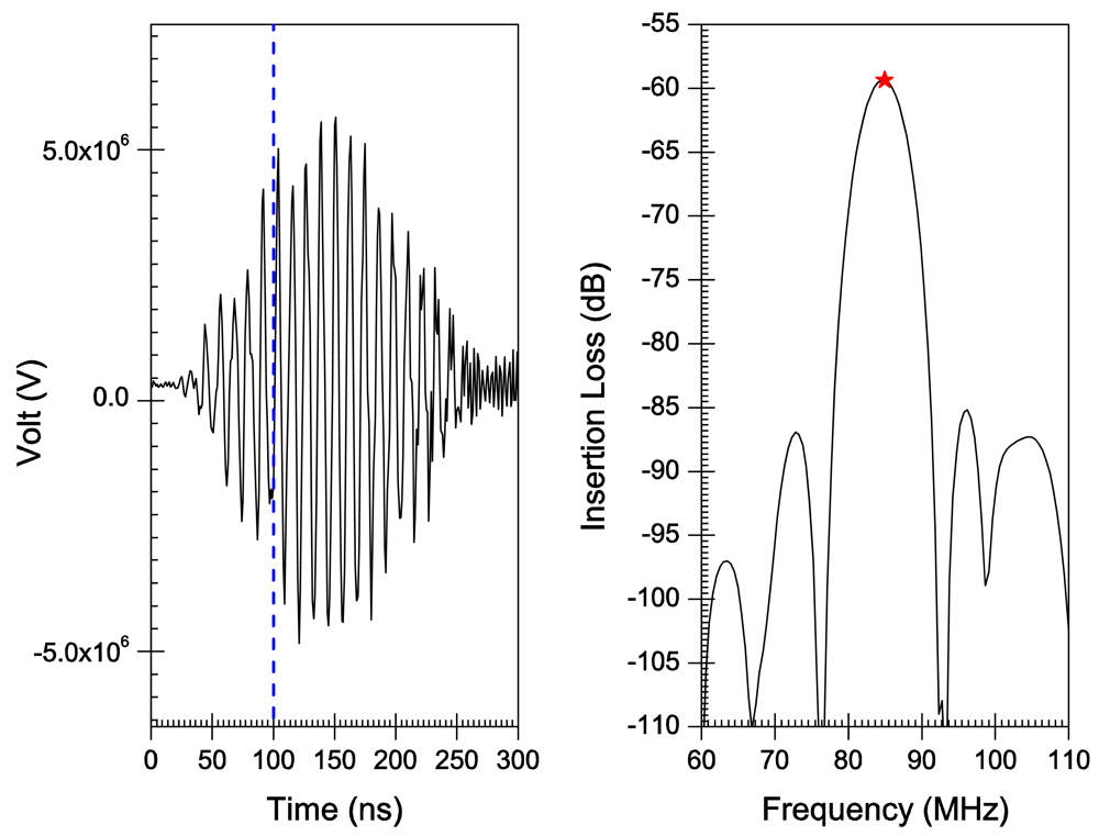
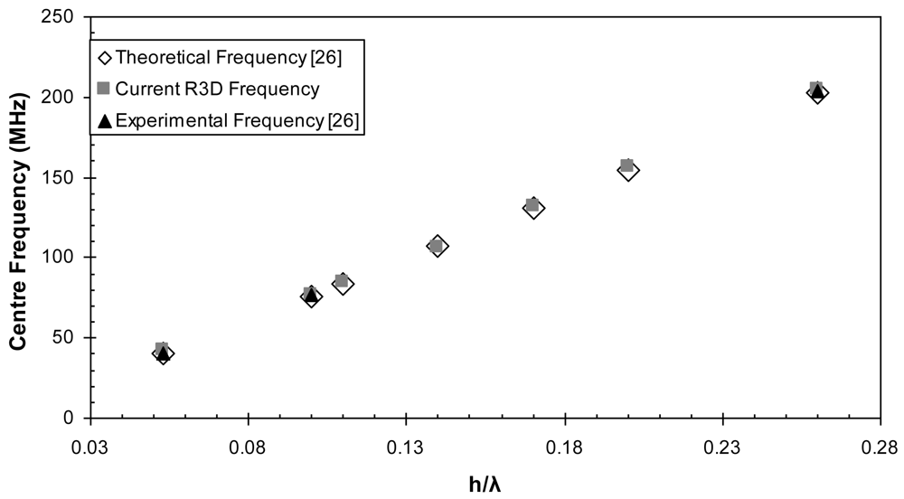
5. Results
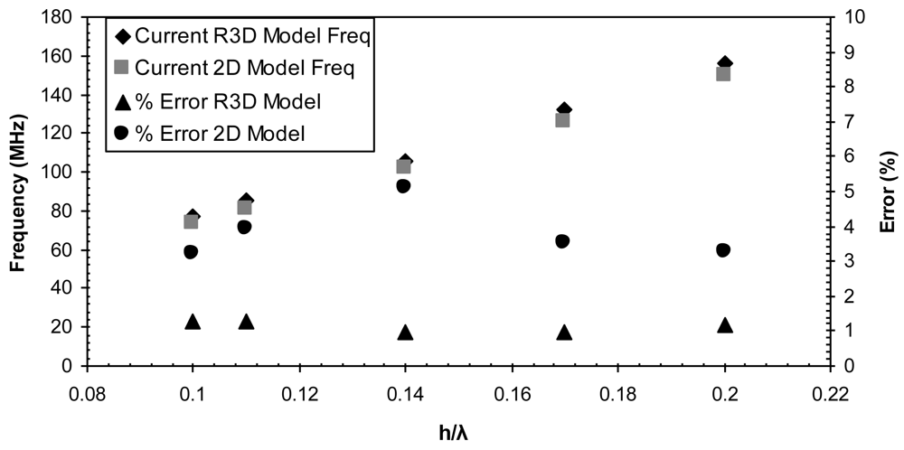
6. Discussion
7. Conclusions
Acknowledgments
References and Notes
- Liu, Y.; Cui, T. Power Consumption Analysis of Surface Acoustic Wave Sensor Systems Using ANSYS and PSPICE. Microsyst. Technol. 2007, 13, 97–101. [Google Scholar]
- Anisimkin, V.I.; Penza, M.; Valentini, A.; Quaranta, F.; Vasanelli, L. Detection of Combustible Gases by Means of a ZnO-on-Si Surface Acoustic Wave Delay Line. Sens. Actuat. B 1995, 23, 197–201. [Google Scholar]
- Hoummady, M.; Bastien, F. Acoustic Wave Viscometer. Rev. Sci. Instrum. 1999, 62, 1999–2003. [Google Scholar]
- Lee, K.; Wang, W.; Kim, G.; Yang, S. Surface Acoustic Wave Based Pressure Sensor with Ground Sheilding Over Cavity on 41 YX LiNbO3. Jpn. J. Appl. Phys. 2006, 45, 5974–5980. [Google Scholar]
- Wu, T.T.; Chen, Y.Y.; Huang, G.T.; Chang, P.Z. Evaluation of Elastic Properties of Submicrometer Thin Films Using Slanted Finger Interdigital Transducers. J. Appl. Phys. 2005, 97, 073510:1–073510:5. [Google Scholar]
- Gangadharan, S.; Varadan, V.V.; Jose, K.A.; Atashbar, M.Z. Love Wave Based Ice Sensor. Proceedings of the 1999 Smart Structures and Materials: Smart Electronics and MEMS, Newport Beach, CA, USA, March, 1999; pp. 287–293.
- Campbell, C. Surface Acoustic Wave Devices and Their Signal Processing Applications.; Academic Press: San Diego, CA, USA, 1989. [Google Scholar]
- Plessky, V. Coupling of Modes Analysis of SAW Devices. Int. J. High Speed Electron. Syst. 2000, 10, 867–947. [Google Scholar]
- Tobolka, G. Mixed Matrix Representation of SAW Transducers. IEEE Trans. Sonics Ultrason. 1979, SU-26, 426–428. [Google Scholar]
- Allik, H.; Hughes, T. Finite Element Method for Piezoelectric Vibration. Int. J. Numer. Methods Eng. 1970, 2, 151–157. [Google Scholar]
- Lerch, R. Simulation of Piezoelectric Devices by Two- and Three-Dimensional Finite Elements. IEEE Trans. Ultrason., Ferroelectr. Freq. Control 1990, 37, 233–247. [Google Scholar]
- Atashbar, M.Z.; Bazuin, B.J.; Simpeh, B.M.; Krishnamurthy, S. 3-D Finite Element Simulation Model of SAW Palladium Thin Film Hydrogen Sensor. Proceedings of IEEE International Ultrasonics, Ferroelectrics and Frequency Control, Montréal, Canada, August, 2004; pp. 549–553.
- Ippolito, S.J.; Kalantar-Zadeh, K.; Wlodarski, W.; Matthews, G.I. The Study of ZnO/XY LiNbO3 Layered SAW Devices for Sensing Applications.
- Botkin, N.; Schlensog, M.; Tewes, M.; Turova, V. A Mathematical Model of a Biosensor. Proceedings of International Conference on Modeling and Simulation of Microsystems, Hilton Head Island, SC, USA, March, 2001; pp. 231–234.
- Xu, G. Direct finite-element analysis of the frequency response of a Y-Z lithium niobate SAW filter. Smart Mater. Struct. 2000, 9, 973–980. [Google Scholar]
- Xu, G.; Jiang, Q. A finite element analysis of second order effects on the frequency response of a SAW device. J. Intell. Mater. Syst. Struct. 2001, 12, 69–77. [Google Scholar]
- Abdollahi, A.; Jiang, Z.; Arabshahi, S.A. Evaluation on Mass Sensitivity of SAW Sensors for Different Piezoelectric Materials Using Finite-Element Analysis. IEEE Trans. Ultrason., Ferroelectr. Freq. Control. 2007, 54, 2446–2455. [Google Scholar]
- Ippolito, S.J.; Kalantar-Zadeh, K.; Powell, D.A; Wlodarski, W. A 3-Dimensional Approach for Simulating Acoustic Wave Propagation in Layered SAW Devices. Proceedings of IEEE International Ultrasonics Symposium, Honolulu, HI, USA; 2003; pp. 303–306. [Google Scholar]
- Atashbar, M.Z.; Bazuin, B.J.; Simpeh, B.M.; Krishnamurthy, S. 3D FE Simulation of H2 SAW Gas Sensor. Sens. Actuat. B 2005, 111-112, 213–218. [Google Scholar]
- Wong, K.Y.; Tam, W.Y. Analysis of the Frequency Response of SAW Filters using Finite-Difference Time-domain Method. IEEE Trans. Microwave Theory Tech. 2005, 53, 3364–3370. [Google Scholar]
- Wu, S.; Wu, L.; Chang, J.H.; Chang, F.C. SAW Modes on ST-X Quartz with an AlN Layer. Mat. Lett. 2001, 51, 331–335. [Google Scholar]
- Jin, Y.; Joshi, S. Propagation of a Quasi-Shear Horizontal Acoustic Wave in Z-X Lithium Niobate Plates. IEEE Trans. Ultrason. Ferroelectr. Freq. Control 1996, 43, 494–494. [Google Scholar]
- Powell, D.A.; Zadeh, K.K.; Wlodarski, W. Numerical Calculation of SAW Sensitivity: Application to ZnO/LiTaO3 Transducers. Sens. Actuat. A 2004, 115, 456–461. [Google Scholar]
- Hietala, V.M.; Casalnuovo, S.A.; Heller, E.J.; Wendt, J.R.; Frye-Mason, G.C.; Baca, A.G. Monolithic GaAs Surface Acoustic Wave Chemical Microsensor Array. Proceedings of IEEE MTT-S International Microwave Symposium Digest, Boston, MA, USA; 2000; pp. 1965–1968. [Google Scholar]
- Hickernell, F.S.; Zinc, Oxide. Films for Acoustoelectric Device Applications. IEEE Trans. Sonics Ultrason. 1985, SU-32, 621–629. [Google Scholar]
- Caliendo, C.; Imperatori, P.; Cianci, E. Structural Morphological and Acoustic Properties of AlN Thick Films Sputtered on Si(001) and Si(111) Substrates at Low Temperature. Thin Solid Films 2003, 441, 32–37. [Google Scholar]
- Mason, W.P. Physical Acoustics Principles and Methods; Academic Press: New York, NY, USA, 1972; Volume 9. [Google Scholar]
- Tiersten, H.F. Hamilton's Principle for Linear Piezoelectric Media. Proc. IEEE. 1967, 55, 1523–1524. [Google Scholar]
- Madou, M.J. Fundamentals of Microfabrication., 2nd ed.; CRC: Boca Raton, FL, USA, 2002. [Google Scholar]
- Tsubouchi, K.; Mikoshiba, N. Zero Temperature Coefficient SAW Devices on AlN Epitaxial Films. IEEE Tran. Sonics Ultrason. 1985, SU-32, 634–644. [Google Scholar]
- Caliendo, C.; Verona, E.; Cimmino, A. Microwave frequency acoustic resonators implemented on monolithic Si/AlN substrates. Proc. SPIE. 2001, 4407, 423–430. [Google Scholar]


| Elastic Matrix in Stiffness Form (× 1011 Pa) | Piezoelectric Matrix at Constant Strain(C/m2) | Permittivity Matrix at Constant Strain (×10-11 F/m) | |||
|---|---|---|---|---|---|
| C11 | 3.45 | e15 | –0.48 | ε11 | 8 |
| C12 | 1.25 | e31 | –0.58 | ε33 | 9.5 |
| C13 | 1.2 | e33 | 1.55 | ||
| C33 | 3.95 | ||||
| C44 | 1.18 | ||||
| C66 | |||||
| Parameter | Value |
|---|---|
| Dimensions of the Si(111) Substrate | 3,000 × 500 × 11 μm |
| Dimensions of the AlN Substrate | 3,000 × 6 × 11 μm |
| Number of Electrode Pairs | 10 |
| Electrode width and Spacing | |
| Separation Distance | 2λ |
| Thickness of AlN Film | 6 μm |
| h/λ | h(μm) | Lambda(λ) (μm) | VTh(m/s) | FTh(MHz) | FExp (MHz) | FSim (MHz) |
|---|---|---|---|---|---|---|
| 0.053 | 6 | 113.2 | 4567.62 | 40.35 | 40.03 | 42.48 |
| 0.1 | 6 | 60.00 | 4570 | 76.17 | 77.12 | 77.15 |
| 0.11 | 6 | 54.55 | 4575 | 83.88 | 84.96 | |
| 0.14 | 6 | 42.86 | 4,586.67 | 107.02 | 105.96 | |
| 0.17 | 6 | 35.29 | 4,608.3 | 130.57 | 131.84 | |
| 0.2 | 6 | 30.00 | 4,633.33 | 154.44 | 156.25 | |
| 0.26 | 6 | 23.00 | 4716.8 | 202.5 | 204.061 | 205.078 |
| Reduced 3D Model Fsim (MHz) | 2D Model Fsim (MHz) | |
|---|---|---|
| 0.1 | 77.15 | 73.73 |
| 0.11 | 84.96 | 80.566 |
| 0.14 | 105.96 | 101.56 |
| 0.17 | 131.84 | 125.97 |
| 0.2 | 156.25 | 149.41 |
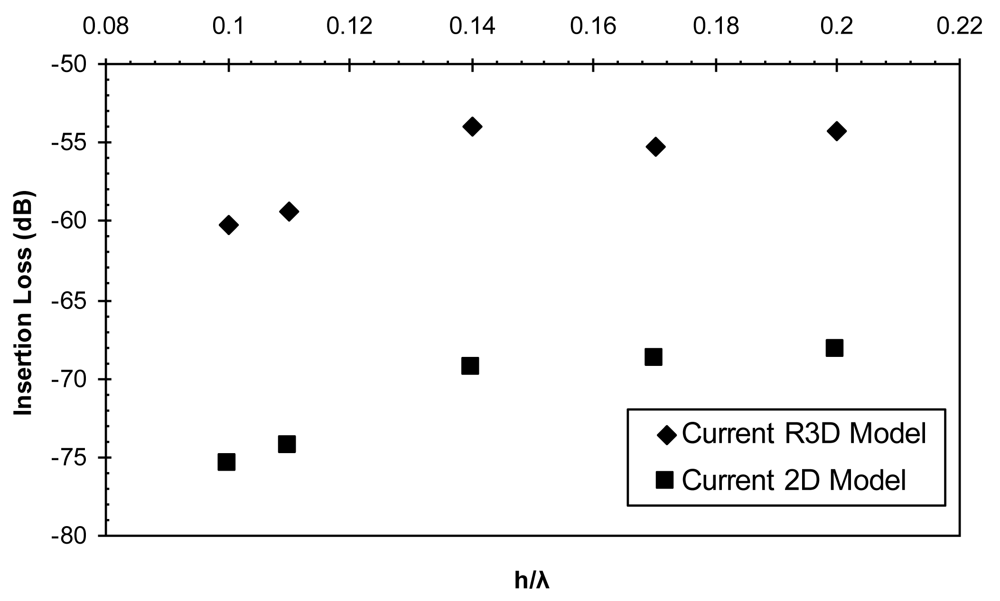
| Reduced 3D Model IL(dB) | 2D Model IL(dB) | |
|---|---|---|
| 0.1 | –60.245 | -75.444 |
| 0.11 | –59.363 | -74.358 |
| 0.14 | –53.98 | -69.315 |
| 0.17 | –55.30 | -68.80 |
| 0.2 | –54.30 | -68.15 |
© 2009 by the authors; licensee Molecular Diversity Preservation International, Basel, Switzerland. This article is an open access article distributed under the terms and conditions of the Creative Commons Attribution license (http://creativecommons.org/licenses/by/3.0/).
Share and Cite
El Gowini, M.M.; Moussa, W.A. A Reduced Three Dimensional Model for SAW Sensors Using Finite Element Analysis. Sensors 2009, 9, 9945-9964. https://doi.org/10.3390/s91209945
El Gowini MM, Moussa WA. A Reduced Three Dimensional Model for SAW Sensors Using Finite Element Analysis. Sensors. 2009; 9(12):9945-9964. https://doi.org/10.3390/s91209945
Chicago/Turabian StyleEl Gowini, Mohamed M., and Walied A. Moussa. 2009. "A Reduced Three Dimensional Model for SAW Sensors Using Finite Element Analysis" Sensors 9, no. 12: 9945-9964. https://doi.org/10.3390/s91209945
APA StyleEl Gowini, M. M., & Moussa, W. A. (2009). A Reduced Three Dimensional Model for SAW Sensors Using Finite Element Analysis. Sensors, 9(12), 9945-9964. https://doi.org/10.3390/s91209945