1. Introduction
Wide band gap (WBG) power devices are dictating the pace of development of power electronics today. There has been considerable advancement in the field of WBG semiconductor power devices. These have the benefits of enabling a high power density at high junction temperatures, coupled with faster switching speeds as compared with their silicon (Si) counterparts [
1,
2,
3,
4,
5,
6]. Thus far, silicon carbide (SiC) [
1,
2,
3] and gallium nitride (GaN) [
4,
5,
6] have been the materials of choice for most WBG modules. While GaN is the preferred choice in applications requiring <500 V, SiC excels in applications exceeding 900 V. SiC devices rated 900 V and above are available in chip sizes spanning just tens of square millimeters. In addition, the switching losses associated with SiC are much lower than the values reported for silicon power devices. SiC devices can be switched at higher frequencies resulting in filtering circuits that occupy less package real estate than their silicon counterparts.
Contributing further to the cause of power density is the fact that WBG devices may operate at high junction temperatures, thus introducing the possibility of employing more volumetrically efficient thermal management schemes. This combination can have a great impact on system miniaturization to help realize system architectures that do not even exist at the present time [
7]. Although the properties of WBG materials seem almost too good to be true at first glance, the realized performance of these power devices are only as good as the package design. Even as the die sizes of the WBG power devices are continually shrinking and the performance is improving, packaging technology is not keeping pace with these developments.
In a modern power electronics module, the size of the passive components and thermal management dictate the overall size. The power stage typically occupies a small fraction of the total volume. This, coupled with weak interconnections using wire bonds, introduces a spate of opportunities for improvement. In fact, eliminating wire bonds and designing shorter interconnects with lower parasitics itself could lead directly to a reduction in the size of passive circuit elements.
3D packaging has always been an attractive buzzword in the world of electronics packaging [
8,
9,
10,
11]. Most of the efforts in this area have been largely focused toward microelectronics, but the benefits translate to higher power modules as well [
12]. However, it is necessary to take a step back and critically evaluate the need for a 3D approach and weigh it carefully against any foreseen disadvantages. It has been mentioned before that even in current state-of-the-art multi-chip modules (MCMs), coefficient of thermal expansion (CTE) mismatch of a single interface is a cause of concern—3D electronics packaging takes this problem and literally multiplies it by the number of tiers in the design. This poses the threat that 3D electronics packaging may open a plethora of design challenges.
The immediate benefits of using a 3D topology are clearly apparent—a reduction in parasitics, use of efficient distributed cooling schemes, a reduction in footprint and consequent increase in power density. However, caution should be exercised regarding the implementation of such a scheme and the ramifications it may have on the overall system performance. The question being asked here is: are we solving a problem, or trading one problem for a host of others?
Research in electronics packaging over the past two decades bears testimony to the desire to move away from wire bonding as an interconnection method [
13,
14,
15,
16]. There have been several attempts to propose alternative methods, and many of these will be investigated in this paper in due course. Most of the methods reported a decrease in the parasitic inductance in the critical switching loops and projected a relative increase in reliability as compared with modules having wire bonded interconnections.
The packaging of SiC power devices are deeply rooted in the wire bonding approach used for silicon metal-oxide-semiconductor field-effect transistors (MOSFETs) and insulated gate bipolar transistors (IGBTs). Wire bonding has been the standard approach used in MCMs because of ease-of-use and low production costs. As far as performance of an interconnect goes, parasitic inductance, reliability, and cost/manufacturability are the major parameters. Wire bonds offer a significant parasitic inductance; however, it does not manifest itself too adversely at switching frequencies ranging up to tens of kHz. Since most commercially available silicon power modules are well within this specification, switching transients resulting from the parasitic inductance of a wire bond are still within tolerable limits. However, the situation is very different with WBG devices which have shown promise at frequencies exceeding 1 MHz. It is for this reason that many GaN manufacturers have adopted a land grid array (LGA) or ball grid array (BGA) approach in favor of wire bonding. On the down side, the reliability concerns of such approaches have prevented a wide-spread adoption of these techniques across the WBG industry.
This paper aims at investigating the trends in SiC power packaging over the past decade and highlights some of the high-performance modules.
Section 2 summarizes the chief requirements of SiC packaging. From a survey of these advanced wire bonded SiC modules in
Section 3, the major technology bottlenecks for the further advancement of SiC packaging technology are assessed.
Section 4 makes a case for wire bondless packaging. Investigations into previous work in silicon 3D wire bondless packaging are presented in
Section 5. Some of the more recent 3D integration efforts in SiC modules are described in
Section 6, followed by a summary of future efforts and directions in
Section 7.
2. Requirements of Silicon Carbide Packaging
In the case of any power device technology—Si, SiC, or GaN—the goal should be to ensure that the package does not hinder the performance of the device. A common example of this is package parasitics. Through hole and surface mount packages have been standard choices for discrete power devices for an extended period of time. In fact, many high performance power electronics systems still use discrete devices—they are simple to assemble and easy to replace upon failure. Most of these applications used switching frequencies in the range of 1–5 kHz. As packaging materials are added to the package, the electrical path to the terminals increases significantly. Additional parasitic inductance is perhaps the most significant adversity that arises at the result of this. As power MOSFETs were introduced and became popular, the major manufacturers began making power devices available in bare die form. This offered power module designers more flexibility to minimize parasitics and increase power density. This became especially important as switching frequencies increased. Switching frequencies up to 25 kHz are becoming increasingly common for SiC power modules. This requires a more thoughtful consideration with respect to module layout and interconnect technologies. Some practices, such as including a Kelvin source terminal for the gate driver return path, have become extremely helpful for SiC module design. Some manufacturers like Wolfspeed have also been including an additional Kelvin source terminal with their discrete devices as well.
SiC power devices have the potential to impact power density at all levels in the package—a reduction in the size and number of power devices, a reduction in the size and number of passives for filtering circuits, and a reduction in the volume of thermal management [
1]. The advent of high voltage SiC power devices will eliminate the need to parallel a large number of power die. This will reduce system complexity and improve system reliability. However, a careful examination is required to be able to assess the requirements of SiC packaging.
Although measures are being taken to reduce the critical switching loop parasitics in SiC power modules, it must be acknowledged that wire bonds are one of the major causes of parasitics. Even a short wire bond has an inherent parasitic inductance that often dominates the total parasitic inductance of the entire loop [
2]. These stray inductances do not affect the circuit if the switching frequencies are low enough. Considering that the switching losses of Si power devices increased significantly with switching frequency, rudimentary parasitic minimization strategies provided satisfactory electrical performance. However, despite having relatively lower switching frequencies the overshoot arising from the power loop parasitic inductance ensured that selected power devices had to be over-rated to able to accommodate this.
Meade conducted a detailed study on the parasitic problem in 2008 [
3]. A simple DC-DC converter topology was chosen to demonstrate the effect of parasitic loop inductances on electrical performance. The turn-off losses dominated, especially as the switching frequency approached 2 MHz. A drastic reduction of the turn-off losses was demonstrated for a wire bond-less packaging method at 3 MHz switching frequency. The losses were much worse for discrete devices. Traditional wire bonded techniques resulted in nearly twice the turn-off losses as compared with the wire bond-less technique. Another interesting fact was that paralleling wire bonds does not alleviate he parasitic problem. The mutual inductance between adjacent wires starts dominating, and there is a limit to which increasing the number of wire bonds can help—a fact presented in a 2016 publication by Yang [
17]. Wire bond-less packaging must be pursued as a thrust area for SiC packaging if high voltages and currents are desired to be switched at several MHz. However, faster switching would directly translate to a risk of producing greater electromagnetic interference (EMI), and caution must be exercised to prevent this.
EMI suppression is another cardinal aspect of package design that has assumed importance owing to rising dv/dt rates in power electronic circuits. One of the common design philosophies which we will encounter in due course is to integrate the gate driver circuit closer to the power device to form low-area switching loops to reduce parasitics. Although this is the correct approach in principle, high slew rates introduce injected current spikes through the parasitic capacitances in the circuit. Future SiC modules must take this into account. As gate drivers and decoupling capacitors are included in the module itself, care should be taken to decouple spurious current spikes from influencing false turn-on events and leading to premature module failure.
From the viewpoint of thermal design, there are two principal thrust areas: (1) thermo-mechanical design strategies for low stress and high reliability; and/or (2) double-sided cooling methodologies. While the first area is advantageous regardless of package type, the latter depends on the critical performance criteria for a given module.
There has been a substantial amount of work in identifying and developing materials having a close CTE match with SiC. Many of the approaches are discussed in this paper in due course. Die attach failure and interconnect failure are among the chief ways in which CTE mismatch manifests itself. This may be attributed to the CTE of a wire bond or bond pad being significantly different as compared with SiC. Another common location at which delamination occurs is the interface between the substrate and heat spreader (or heat sink). Some of the solutions that have been proposed to address these issues are using compliant mechanical materials like sintered silver as the die attach material. The “sponge-like” nature of this material makes it adept at cushioning CTE mismatch stresses. Other methods include the development of alloys and metal-matrix composite materials like MoCu or AlSiC. The CTE of these materials are very well matched to SiC and can be tailored by altering the composition of the compounds. These materials are easy to plate and bond to both the devices and heat sinks (or baseplates).
Double sided cooling is another option in order to reduce thermo-mechanical stresses. If the junction temperature is controlled to a low enough value, CTE mismatch stresses will not adversely impact module reliability. However, a double-side cooled module necessitates a wire bond-less packaging approach. Double-sided cooling is also advantageous in modules employing a large number of chips. This may be a very good proposition for vehicle under hood applications, where the ambient temperature is already at elevated levels. A single-sided cooling solution may simply not be enough to handle the thermal load.
While we are on the issue of thermal performance, there is an important factor to consider. Contemporary Si devices are rated to operate at a junction temperature of 175 °C. Most commercially available SiC devices are also rated for a similar temperature range, although researchers have been able to demonstrate a decent performance at higher temperatures as well. The theoretical limit of SiC as a semiconductor material is well beyond 500 °C. Yet the ratings of commercially available devices do not reflect this advantage. One issue could be the reliability of the chip metallization at elevated temperatures—an extremely valid concern. However, there are other factors at play here. These concerns have been echoed in a 2009 publication by Wrzecionko [
18]. They demonstrated that although the theoretical limit for the operation of SiC power devices can be as high as 700 °C, in reality the optimum temperature was less than 300 °C. The authors were of the opinion that if a device is operated below the optimum temperature, it was not possible to take complete advantage of the junction gate field-effect transistor (JFET). A higher than optimum temperature of operation, on the other hand, ran the risk of thermal runaway. The paper also demonstrated that the power density could be improved greatly by either using a chip with a larger area and/or using double-sided cooling. Both the suggested methods were prescribed with the intention of reducing the thermal resistance. This particular study involved SiC JFETTs, but the same concerns are applicable to MOSFETs as well. A cooler junction temperature also has a positive influence on module reliability.
One of the other concerns of SiC packaging is the metallization of the bare die power devices. The surface finish for all SiC power devices is aluminum for the top side bond pads. This is understandable, since aluminum wire bonding is one of the most widely used means of interconnection. The bottom side finish is usually silver to aid wetting during the soldering process. The silver finish also facilitates advanced die attachment processes like silver sintering. To be able to implement wire bond-less procedures, a reliable and solderable top surface finish is required. One way to circumvent this issue is the use of pressure contacts on the top pads. However, there may be contact resistance issues using these methods that may need to be addressed. A metallurgical bond will require the top side finish to be a solderable metal. This may be done during device fabrication, or re-engineered during the assembly process by incorporating a plating, evaporation, or sputtering test. Electroless Ni/Ag has been a standard plating process for rendering IC chips solderable in the past, and it could work for power devices as well. However, there is no evidence to address the long term reliability of these approaches, especially in high temperature environments. There is no clear answer for an optimized metallization stack up that can attain the same thermal performance standards that SiC devices have been reported to have.
Material concerns should not be limited to metallization alone. Interconnects and encapsulation materials should also withstand comparable thermal stresses. Perhaps the most exhaustive subject of thermo-mechanical stress analysis has been die attach materials. This is perhaps because the die attach interface is both electrically and thermally critical, and extremely prone to cracking under thermal stress. There are analytical models of die attach materials and long-term reliability prediction algorithms based on these models. However, as the operating temperature rises, all parts of the package will assume importance and have to be thoroughly studied before it can be incorporated into a commercial product.
3. Trends in Wire Bonded Silicon Carbide Packaging
SiC power devices have been predicted to have tremendous potential to be the next generation material in the semiconductor industry [
1,
2,
3,
19,
20,
21]. These devices have been shown to operate in extremely high ambient temperatures with very low degradation in performance [
22]. The packaging methods employed for SiC power modules, however, have not witnessed much change from the traditional silicon die attach and wire bond process flow.
This was not considered to be a huge obstacle until recently, since the SiC material system itself was found to be much superior to silicon. SiC devices performed much better than their Si counterparts, even while using standard packaging approaches. However, as engineers around the world are gaining a better understanding of SiC devices, the limits of the Si-based packaging schemes are becoming more evident. Most of these packaging approaches bear fundamental performance limits imposed by the physical limits of Si device physics. For example, wire bonding has sufficed as an interconnect technology in modules that switched at the safe operating limits of SiC power devices. Similarly, CTE mismatch stresses were tolerable in Si power modules, most of which were rated at much lower maximum operating temperatures as compared with SiC. As SiC power devices are demonstrated to operate in ambient temperatures pushing the 500 °C mark, most Si power module material choices will be rendered unusable. Nevertheless, even without employing unconventional and “out-of-the-box” packaging methods, SiC packaging efforts over the years have successfully demonstrated some noteworthy feats.
A 2007 study from Arkansas Power Electronics International (APEI) Inc. (now Wolfspeed, Fayetteville, AR, USA) documented the test results of a 4 kW three-phase power inverter operating at a junction temperature of 250 °C [
23]. The design and choice of packaging materials used was a combination of known-good approaches for MCMs using Si IGBTs. The power devices in the module were SiC JFETs. Extending the results to a 10 kW inverter based on an identical approach, the authors predicted a 75% overall decrease in the volume as compared with a comparable Si inverter. One major reason for this was the high temperature operability of the SiC devices, which reduced the requirement of volume-intensive thermal management methods.
Most packages developed around this time did not push the envelope in terms of incorporating novel packaging materials, but there was a growing consensus among industry and academia for the need to think unconventionally to extract maximum benefits.
This issue was addressed in a 2008 paper from General Electric, in which design choices were explored to ensure operation at 250 °C [
24]. Substrates, die, attach materials, interconnects, and encapsulation materials were explored individually. Direct bonded copper (DBC) substrates were observed to fail within the first 20-30 cycles of testing, clearly exposing the need for new substrate technologies at higher temperatures. Sintered thick film silver metallization on alumina performed the best showing no failures up to 1000 thermal cycles. Direct bonded aluminum (DBA) on aluminum nitride also performed comparably and may be a high temperature alternative as well. As far as die attach materials were concerned, it was reported that 95Pb5Sn high temperature solder was good at absorbing CTE mismatch stresses. A novel miniature top-loading laminated bus structure was designed for this module. This enabled a low-inductance path to the power devices, and in-turn allowed them to switch at a faster frequency.
Interconnect inductances were further reduced by using vertical spring-loaded pins instead of wire bonds. The spring-loaded pins were also reported to be more compliant under thermo-mechanical stress. Common epoxy mold compounds did not hold up to partial discharge testing under high temperatures. Nusil and Sylgard were the only compounds that yielded satisfactory performance up to at least 400 h of testing. The temperature for module testing however was limited to 100 °C, and there was no documented data for the system/module reliability with respect to time or temperature.
A more recent study published in 2011 documented the design benefits of SiC power converters over silicon based converters [
25]. In this study, a 1.5 MW wind turbine frequency converter was designed. The first step in this study was a characterization of the switching characteristics of the SiC power device as a function of temperature. It was reported that the switching loss of the SiC device were almost unaffected by temperature, but that for silicon devices the losses increased by 56.3% when the case temperature increased to 125 °C from 25 °C.
The system was also analyzed at switching frequencies of 3 kHz and 50 kHz. At both frequencies, the losses associated with the silicon converter far exceeded the SiC converter. The loss in efficiency for a Si IGBT beyond 20 kHz made it unusable, while the efficiency of the SiC converter even at 50 kHz exceeded 85%. This, of course, introduced possibilities for a significant reduction in the size and cost of the passive circuit elements for the filtering circuitry. The power losses associated with the filtering passives were also reported to decrease.
Another interesting part of this study was high temperature operation of the converters. At an operating temperature of 150 °C the volume of the SiC based converter was substantially smaller than the Si converter. Moreover, the SiC converter did not need liquid cooling, and the overall cost of the heatsink was also much lower than the Si converter. At a junction temperature of 300 °C, the situation improved further for the SiC converter offering a 49.5% additional reduction in volume as compared with the 150 °C converter. Silicon power modules cannot operate at these temperatures, and SiC modules can go even higher with the appropriate packaging choices. Unfortunately, no hardware was tested over time to validate the reliability of operation in a 300 °C ambient.
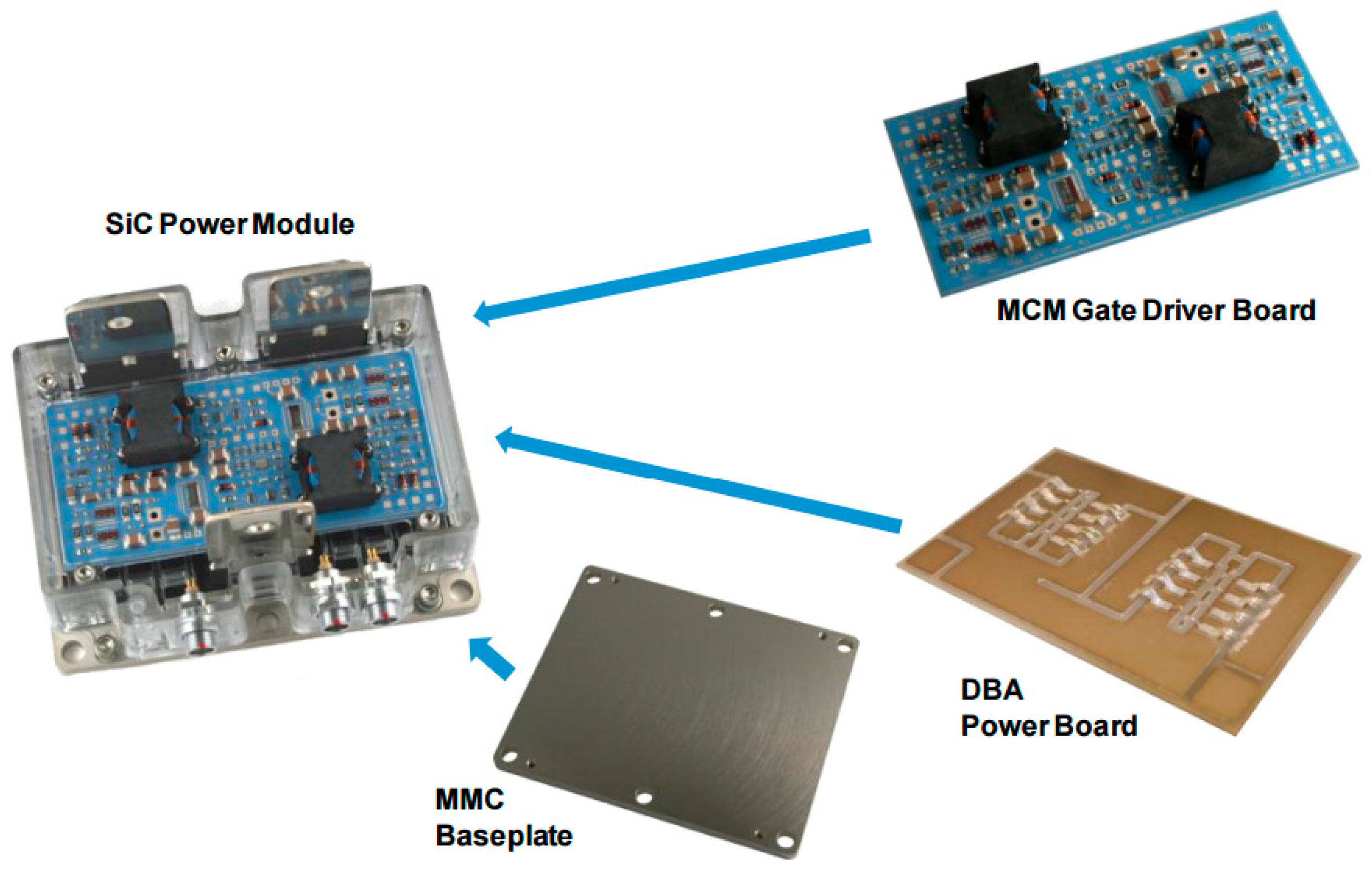
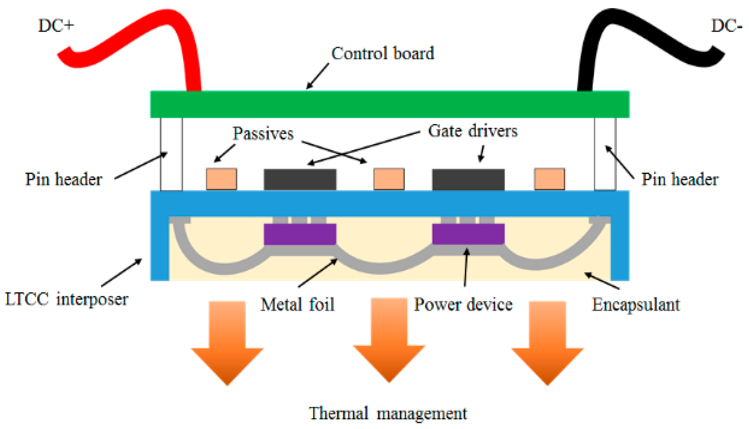
An effort from APEI Inc. in conjunction with the University of Arkansas in 2008 showcased a leap in next generation packaging for SiC modules [
26]. The highly integrated half bridge module (
Figure 1) was capable of operating at 250 °C and also won the R&D 100 award in 2009.
The gate driver board was made of low temperature co-fired ceramic (LTCC) material capable of withstanding high temperatures. The magnetics used were fabricated in-house in order to meet the temperature requirements, and the size of the passives were reduced considerably by driving the half-bridge at 150 kHz switching frequency. To enable an increased switching frequency, the gate driver board was mounted directly atop the power stage to offer a low inductance vertical path for the gate signal. The stacked approach also reduced the footprint of the module, enabling high density integration even at elevated temperatures. As a proposition for future work for reducing the size and enhancing performance, it was discussed that the gate driver would be placed on the power stage to further reduce parasitics.
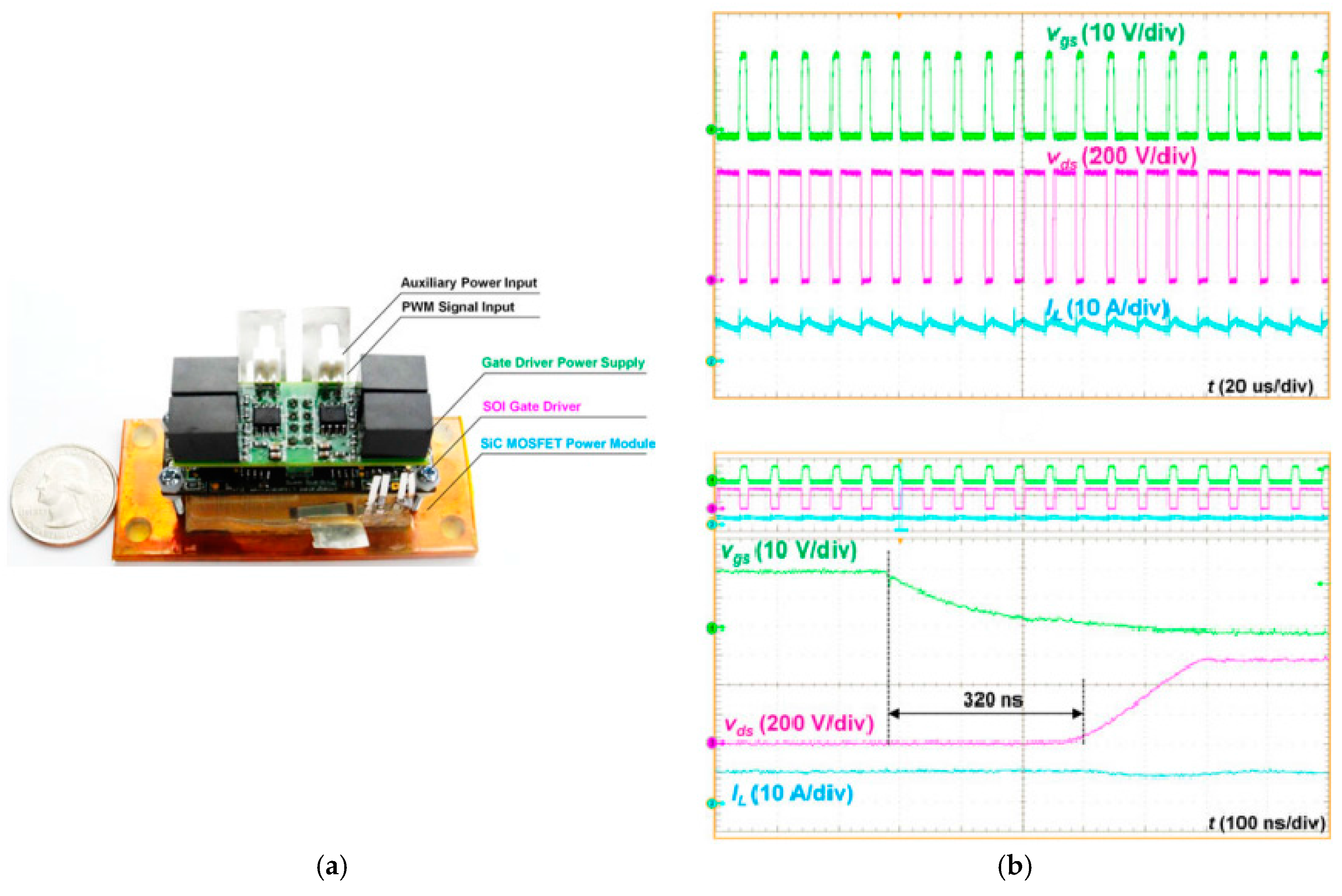
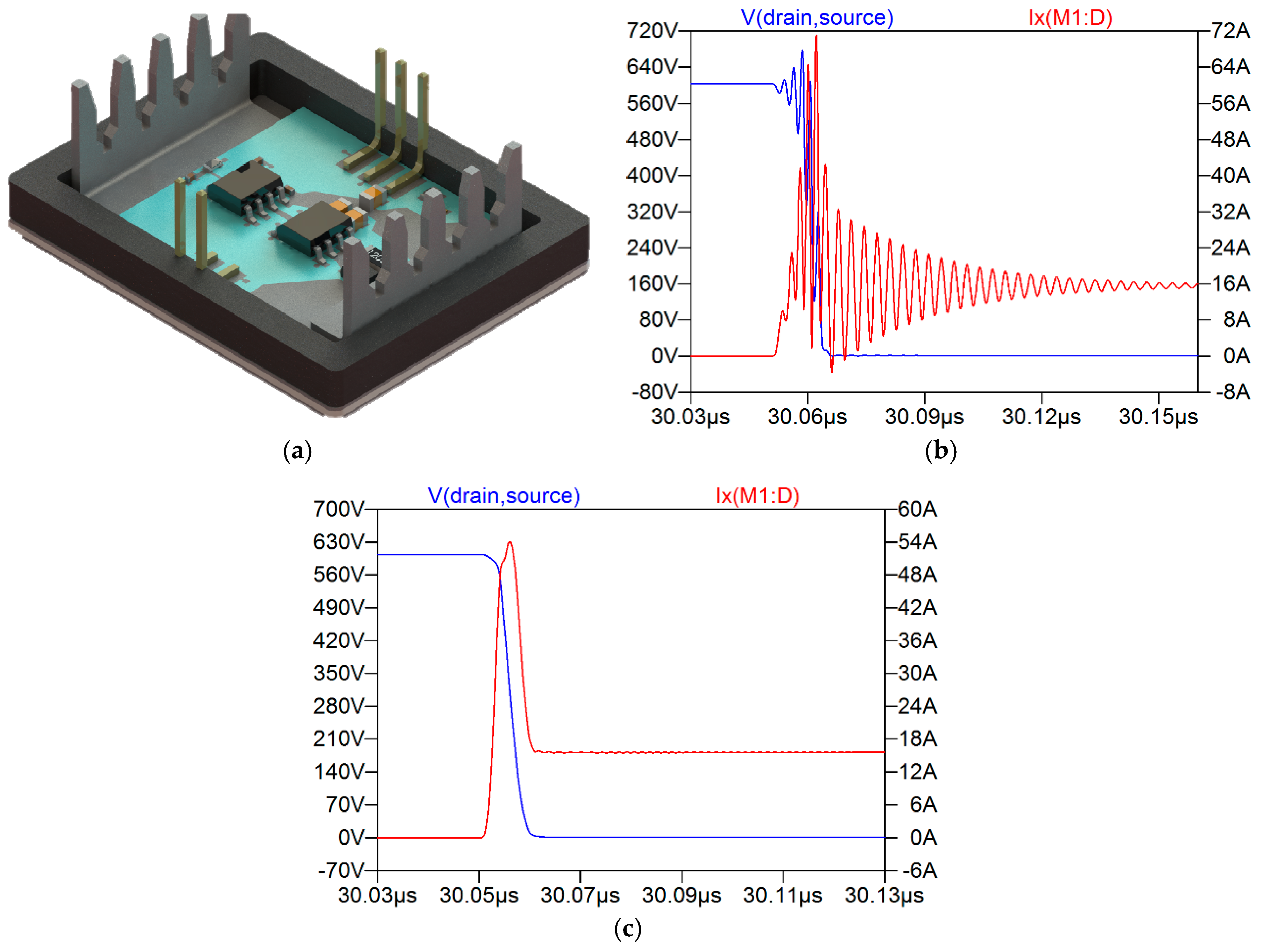
For most applications involving high voltage slew rates at high temperatures, the choice of gate driver becomes a limitation. In many investigations, the SiC module itself was tested inside a high temperature oven, while the gate driver and controls were placed in a lower ambient temperature. This problem was addressed in a 2015 publication by Wang et al. [
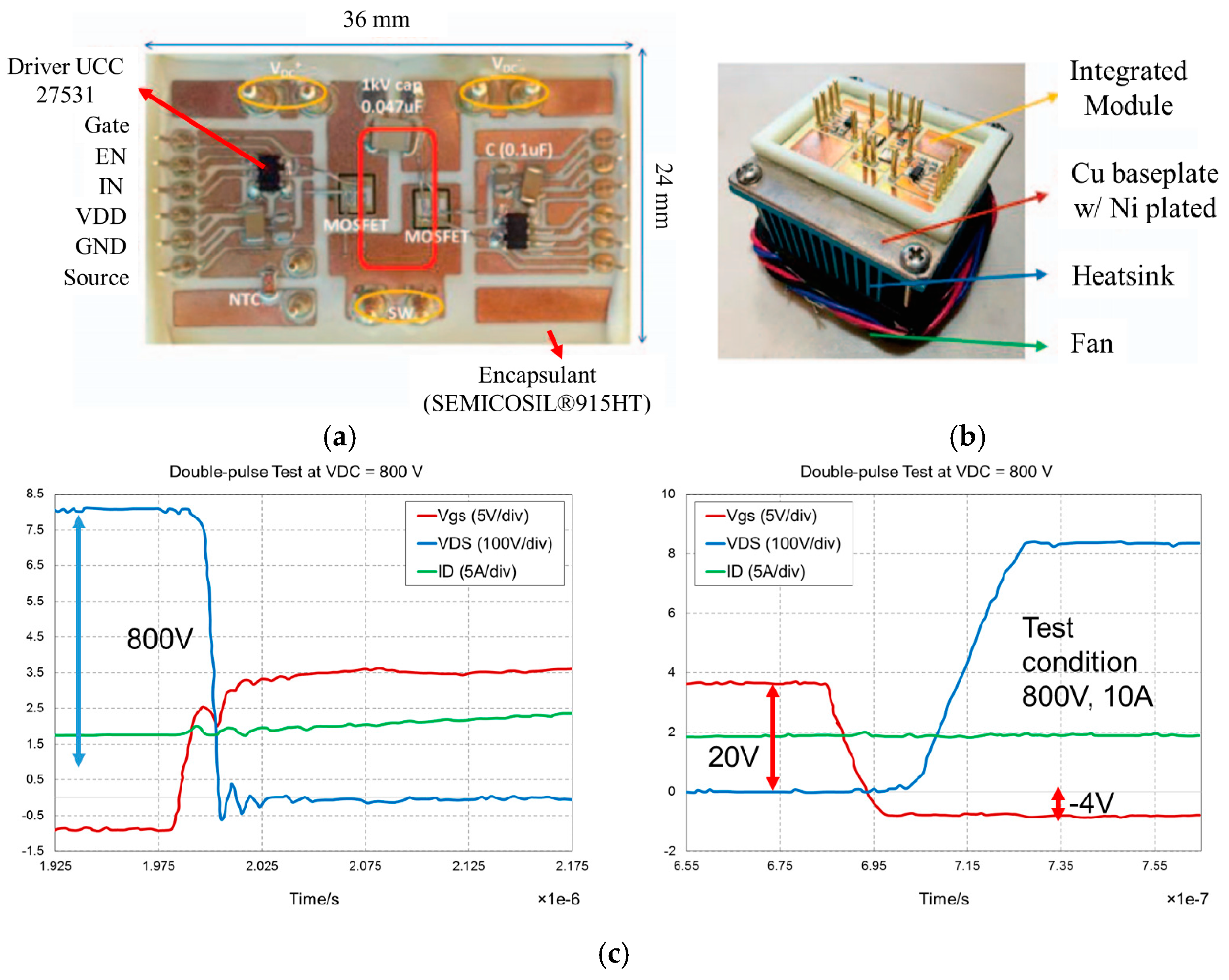
27], in which a silicon-on-insulator (SOI) gate driver was integrated with a SiC power module. The integrated module shown in
Figure 2a was operated at a temperature of 200 °C and a switching frequency of 100 kHz (
Figure 2b). This study brings to light the importance and necessity of gate drivers which match the performance of the SiC power devices. A denser integration of the gate driver and the power devices would mean that the driver chip also experiences similar temperatures as the power die.
From all the above studies, it was clear that the performance of a module is package limited. Not one of the studies investigated revealed that SiC had failed as a material at high temperatures. All the expressed concerns dealt with the dearth of adequate packaging materials and technologies at these temperatures.
The story of the high frequency applications of SiC bear a striking resemblance to the high temperature applications. The material itself can switch well into the MHz range. At these frequency levels, the passives employed may be a fraction of the size compared with what is used today. The overall system cost, volume, weight, and losses will also decrease. However, the system implementation is the bottleneck. A high switching frequency implies a high slew rate for the switching currents and voltages. This induces undesirable current spikes through the parasitic capacitances present within the system, leading to a potential system failure due to a false switching event. This phenomenon discourages applications involving frequencies in excess of several hundred kHz. Nonetheless, switching reliably and efficiently at 50 kHz is in itself a huge improvement over silicon MOSFETs and IGBTs. This section explores notable efforts in pushing toward higher switching frequencies, and aims to identify the barriers that prevented a further increase in frequency.
A 2003 study by Elasser et al. [
28] contrasted the performance of the then novel SiC diode against commercially available silicon diodes. Switching losses during reverse recovery at high d
i/d
t were one of the parameters of comparison, and the performance was compared at room temperature as well as at 150 °C. The circuit was tested in a boost converter topology switched at 100 kHz, with a silicon IGBT. It is important to note that this was a low power application with a 500 W full load, but it was sufficient to illustrate the benefits of SiC technology and the concerns with inferior packaging of SiC devices.
Table 1 lists the results of the analysis. The results showed an order of magnitude decrease in the switching losses associated with the SiC devices. Furthermore, the reduction seemed impervious to an increase in junction temperature, where the losses for the silicon based counterparts nearly doubled with an identical temperature increase.
Several studies have been published since, which have supplemented the favorable recovery characteristics of SiC SBDs. It is hardly surprising that they are ubiquitous in most high performance power modules that are produced today. In 2011, Adamowicz et al. [
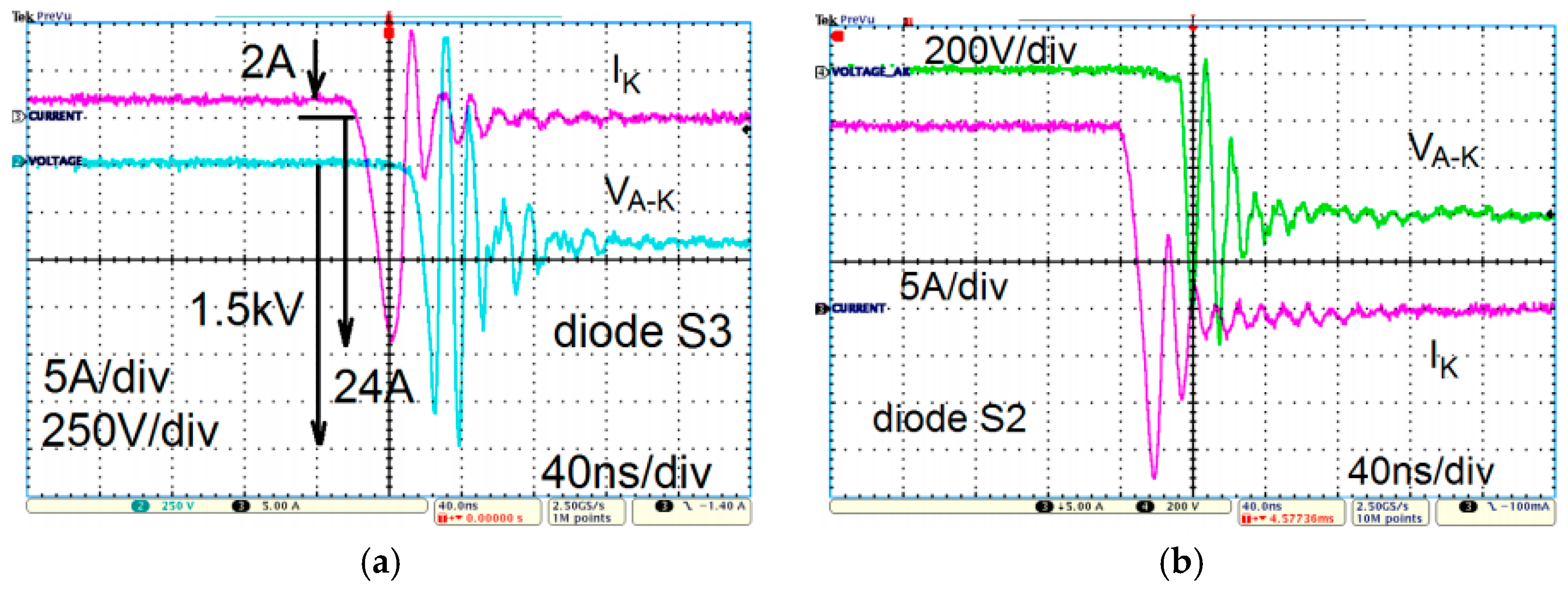
29] conducted a similar study, with a cardinal difference. They fully appreciated the benefits of a near-zero reverse recovery offered by SiC diodes, but with caution toward the implications from the standpoint of EMI. A 100 kHz converter was constructed using SiC JFETs and SiC freewheeling diodes (FWDs). The performance was also contrasted by using a Si FWD in conjunction with the SiC JFETs.
Figure 3a shows the turn-off waveform for the silicon fast diode. The performance was unacceptable at 100 kHz with the reverse recovery current exceeding 24 A while carrying just 2 A. Voltage perturbations were also reported in the test circuit as a result of EMI with magnitudes exceeding 1.5 kV. This could potentially kill power supplies, gate drivers, and even the power devices themselves.
Figure 3b shows the result for one of the SiC diodes under investigation. Oscillations could still be observed in the turn-off waveforms, but were tolerable. An interesting observation was that two diodes with similar characteristics showed slightly different damping on the gate-source signal. It was deduced that the source lead parasitic inductance contributed the gate-source ringing. This is another instance where it was proved yet again that the performance of the SiC device was packaging limited. The estimated lead inductances in the discrete components used for this study were reported to be around 20 nH.
Since this time, most integration efforts have been focused on tighter integration to reduce interconnect inductances and mitigate the EMI arising as a consequence. This is a compelling reason for most major SiC manufacturers providing an additional Kelvin sense terminal in their discrete component packages [
30].
A significant step forward in high frequency operation and its impact on system size and performance was presented in a 2013 publication from APEI Inc. and Toyota, in conjunction with the University of Arkansas [
31]. The illustrated high power density plug in HEV battery charger also won an R&D100 award in 2014. The designed converter was switched at a frequency of 500 kHz and yielded an efficiency of 93.4%. The efficiency increased to 96.5% as a result of decreasing the switching frequency to 200 kHz, which is still an impressive frequency as compared with the competition.
The increase in switching frequency allowed the designers to reduce the size and weight of magnetics and relax the demands required by the heat sink. The result was a volumetric power density of 12 kW/L, and a gravimetric power density of 9.1 kW/kg. The weight was especially important since this module was designed to operate in a mobile system. The researchers reported that customized package design was a key enabler in being able to push the performance of SiC technology closer to what it is capable of. Design improvements included a customized low inductance power module. The gate driver board with the associated circuitry was mounted in close proximity with the power module.
The power module was mounted on a MMC baseplate to reduce the CTE mismatch and weight, and facilitated high temperature operation. Even with these commendable efforts to leverage high frequency operation, the authors reported that the thermal management and the inductors used in the module comprised 73% of the weight, and 66% of the volume respectively. It was discussed that pushing the operating frequency beyond 500 kHz would help further volumetric gains, but it was not clearly stated what prevented the authors from doing so in this revision itself.
In a separate publication in the same year, APEI reported that they had operated the X5 module at frequencies in excess of 1 MHz while maintaining an efficiency greater than 93% up to nearly 4 kW output power [
32]. It was reiterated in the paper that the design philosophy for switching at these unprecedented frequencies relied heavily on tighter integration between the power devices, drive circuitry, and decoupling capacitors.
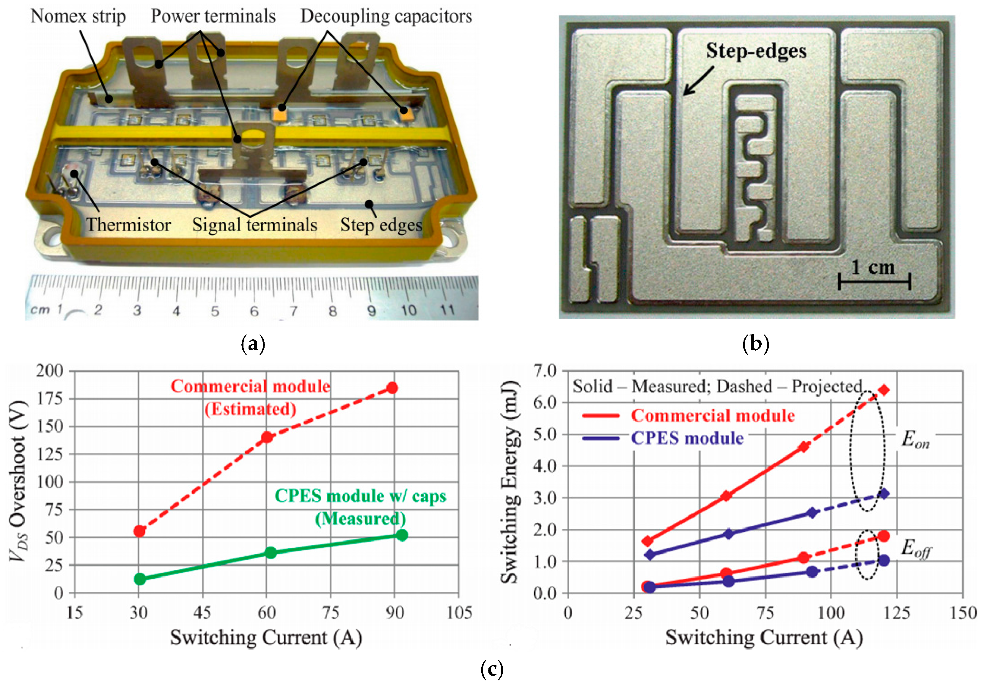
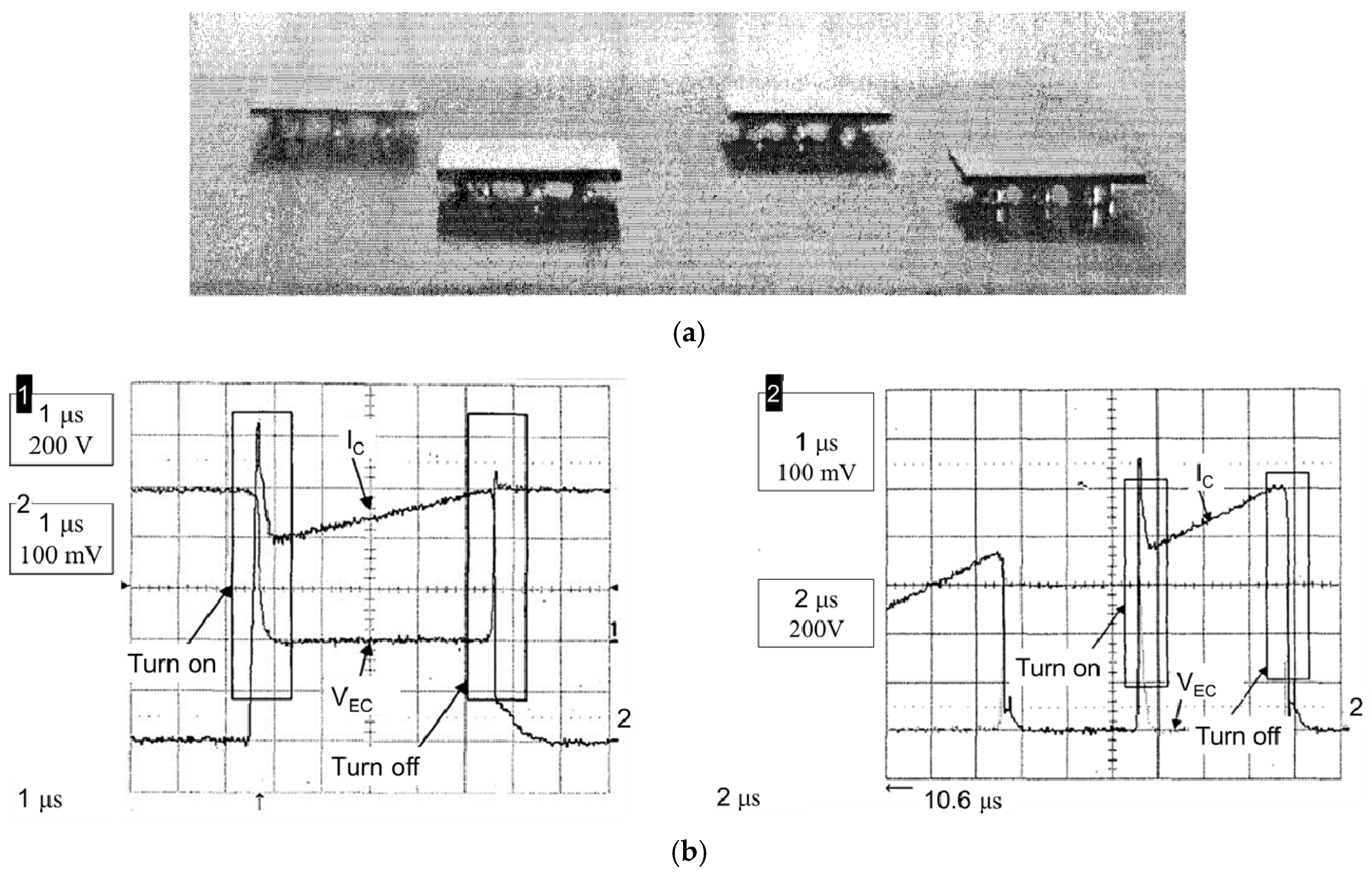
The need for a high temperature and high frequency module was also the underlying motivation for a 1.2 kV, 120 A phase leg module using SiC devices by Chen et al. [
33] in 2016. By optimizing the layout of the module, a 40% reduction in the switching loop inductance was possible, even while using wire bonded interconnections. The module was also demonstrated to operate at 200 °C junction temperature. The power module is shown in
Figure 4a. The substrate used was DBC with AlN as the ceramic—a common material if choice for SiC power modules. However, DBC substrates have gained a negative reputation for delamination during high temperature swings. To remedy this, a step-edge approach was used in which the edges of the copper traces on the DBC were etched so that they formed a tapered step on the edge. This makes the copper less prone to peeling under thermal stress [
34]. A photograph showing the patterned substrate with a step-edge is shown in
Figure 4b.
The parasitic ringing and overshoot for this module were reported to be 20% lower as compared with a commercial module even without embedding decoupling capacitors within the module.
VDS slew rates as high as 13.9 V/ns were achieved with using a 0 Ω external gate resistor due to the favorable switching transient behavior. The overshoots and switching energy comparison is shown in
Figure 4c. No EMI related issues were reported despite the unprecedentedly high voltage slew rates.
Another noteworthy accomplishment in the recent past came from researchers at the Future Renewable Electric Energy Delivery and Management (FREEDM) center (North Carolina State University, Raleigh, NC, USA). The authors in their abstract mentioned with respect to power modules that “The era for high voltage-megahertz switching has arrived [
35].” A 1.5 MHz synchronous boost converter and a 3.68 MHz half bridge inverter were demonstrated.
Figure 5a shows a photograph of the top view of the power module. It can be noticed that the gate drivers for the respective switches were mounted as close as possible to the power die on the power module itself. This resulted in a significant reduction in the gate loop parasitic inductance and prevented false turn on effects due to the EMI generated at the high d
v/d
t levels generated in the circuit.
Figure 5b shows a photograph of the module with the heatsink, and
Figure 5c shows the switching waveforms.
The efforts presented in this section summarize admirable research to place SiC technology a cut above conventional silicon power modules in terms of performance. All the above approaches used existing packaging technologies and materials in novel ways, and employed good engineering practices to develop next generation power electronics modules. However, the achievements still grossly underutilized the full gamut of performance benefits that SiC devices have to offer. One of the key enablers in pushing performance would be the interconnect technology.
Some issues are common for the packaging and integration of any class of semiconductor technology. Heat sinks and passive devices are two examples of such issues. Be it silicon, SiC, or GaN—these components occupy maximum space and weight in the package. Using WBG technology to help relax the demands of a big and heavy heat sink may alleviate the issue from the standpoint of thermal management. It will also encourage innovations in heat sink technology. However, efficiency is really a more dominant concern in power converters. Producing efficient topologies and packaging solutions may not even create substantial waste heat to begin with. This coupled with the high temperature operability of SiC devices have the potential of greatly impacting the volume occupied by the thermal management in a power module. A far as passive devices are concerned, significant reductions in size and weight are possible when switching frequencies are increased, as have been documented by several of the aforementioned research efforts.
4. Wire Bondless Packaging—The Road Forward?
The quality and reliability of power modules has a direct influence on resource utilization, the cost of production, and energy efficiency in the industry. We are at the peak of global electrification, and the trends predict a steady increase in the foreseeable future. The sphere of applications of electronic modules is ever-increasing—and it is perhaps time to move past the “one size fits all” packaging solutions that have been strongly adhered to up to now. Conventional packaging materials and methods have been known to perform poorly under both thermal and electrical stress. Hence, applications involving harsh environments have typically been most accepting of novel packaging technologies. In fact, most innovations pertaining to the field of electronics packaging have been targeted toward applications with harsh temperatures, harsh environments, high power levels, large voltage swings—or any combinations thereof.
In their 2011 paper summarizing the challenges in power packaging, Liu and Kinzer [
36] from Fairchild Semiconductor hailed SiC as a foreseeable future replacement for silicon power devices. However, they agreed that the interconnection scheme had to improve. They discussed alternatives to conventional wire bonding—such as copper ball bonding, wedge bonding, clip connections, copper stud bumps, flip-chip bonding, etc. Many of these approaches will be discussed in due course. They also discussed that as SiC chip sizes shrink, there needs to be effective mechanisms for increased heat transfer. Double-sided cooling can be explored as an example, by adopting wire bondless sandwich-type modules.
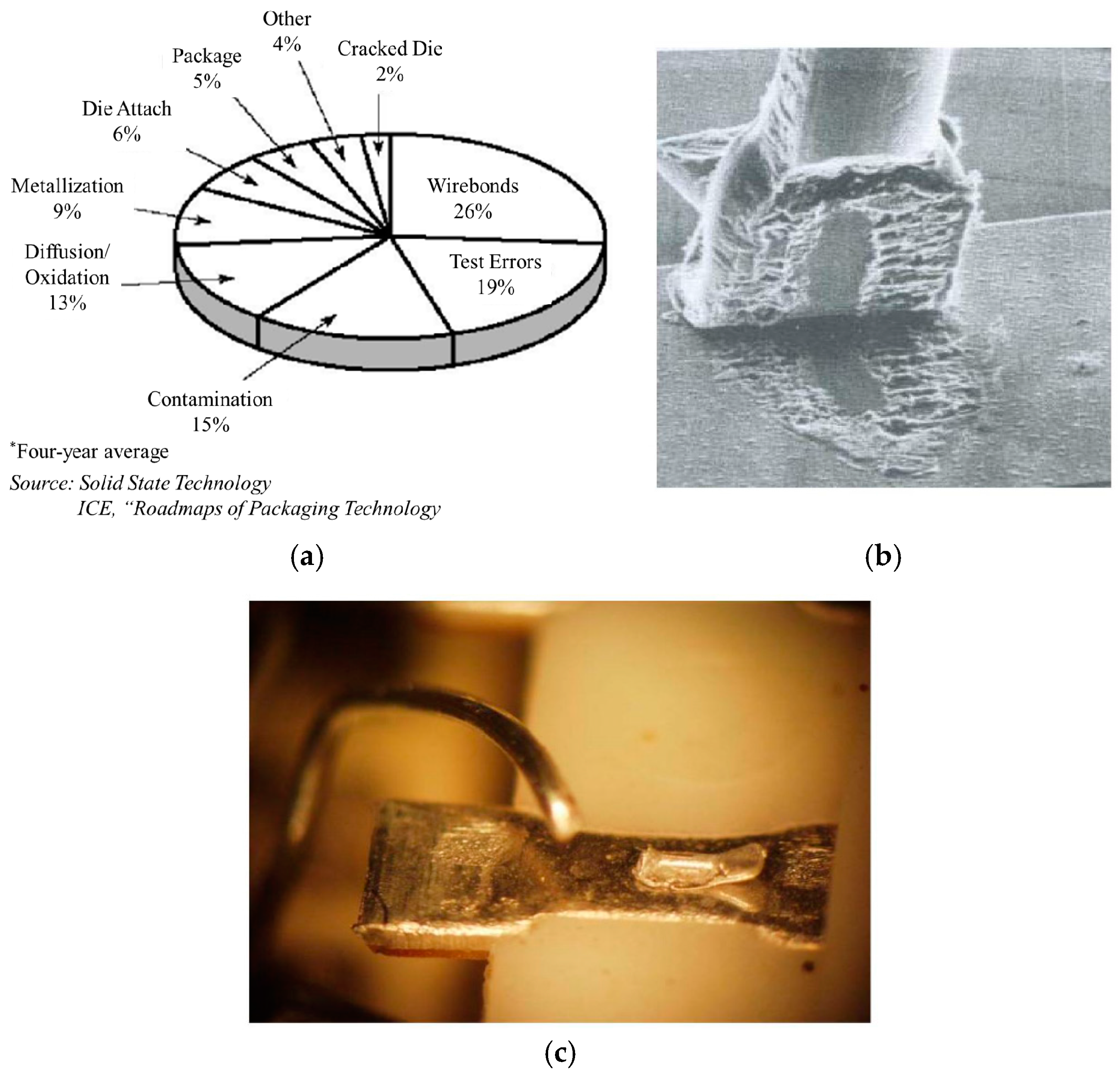
In 2007, Bower et al. [
37] documented some of the common issues that were being reported in relation to the failure of SiC modules. Unsurprisingly, wire bond fatigue topped their list, in itself accounting for the most failures associated with a single component (
Figure 6a).
Figure 6b,c shows the dominant failure mechanisms in wire bonds.
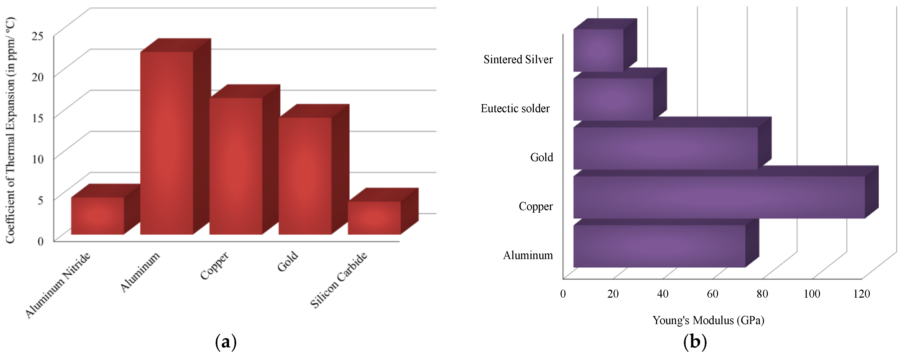
Wire bond lift off occurs due to the same reason that solder interfaces fail—due to CTE mismatch stresses between the bond pad and bonding material. However, the CTE of the metals used for wire bonding differ by a large margin from the substrate materials as shown in
Figure 7a. Hence, they are prone to fail much sooner under repeated thermal stress or high temperature than a solder joint would. In fact, CTE is not all that materials for a thermo-mechanical stress. Even eutectic solder and sintered silver have a high CTE, but they are better at absorbing thermo-mechanical stresses due to their low Young’s modulus.
Figure 7b shows a comparison of the Young’s modulus of wire bonding metals and common die attach materials.
To improve the mechanical strength of wire bonds, some measures have also been taken to utilize thick Cu/Al-Bi ribbon bonding instead of aluminum [
38]. However, like with most copper wire bonding approaches, this has the risk of damaging the die due to excessive bonding force/energy [
36]. Ribbon bonding does not, however, solve the problem of connecting the gate pad of a SiC MOSFET. With the shrinking die sizes of SiC devices, justifying the use of ribbon bonding is going to become increasingly more difficult. Also, any type of wire bonding technology eliminates the possibility of double-sided cooling or 3D integration, which brings us to our next topic.
5. 3D Integration Efforts
There have been several attempts to provide better alternatives to wire bonding through 3D wire bondless technology. Although the industry has adopted a handful of these propositions, most of the proposed solutions exist only as proof-of-concept. The main explanation for this is that the reliability and performance benefits offered by a large majority of these solutions can seldom justify the cost of a complete retooling of a manufacturing facility. If a simple solder and wire bond based module of sufficient engineering quality meets the target module lifetime with satisfactory performance, there is hardly a need to think about 3D solutions. However, this situation is rapidly changing with elevated demands on the performance and operating conditions that power modules are expected to meet. There are numerous other advantages to be realized in a well-engineered and non-conventional packaging scheme—decreased material costs, faster performance, reduced electromagnetic interference, and improved thermal management to name a few. Among the innovative schemes proposed in the last 5–10 years, only a few have managed to successfully transition into a commercial module from a proof-of-concept.
Power electronics packaging has always borrowed liberally from microelectronics packaging advances in the past. Most of the chip-on-board, flip-chip, and 3D through silicon via (TSV) research that exists in the literature is targeted toward low power microelectronics or sensor applications [
39,
40,
41,
42,
43,
44]. Low power RF circuits have also adopted wire bondless BGA-based packaging methods as state-of-the-art due to the parasitic reduction offered by such 3D integration schemes, reduced cost, and reliability benefits [
45,
46,
47,
48]. There is also a wealth of literature in support of the favorable aspects of BGAs. In fact, an application note from Fairchild Semiconductor a silicon BGA package has been described as a step in the direction of realizing the “perfect MOSFET” [
49]. However, in this investigation we only intend to include the advances in 3D/wire bondless power module packaging in detail.
Most of the 3D packaging solutions proposed to date utilize Si devices. These propositions came at a time when Si technology was hitting a limit in terms of performance. Wire bondless integration offered hope from the standpoint of better signal integrity and reliability. The inherent properties of WBG were found to be so much more superior to their existing Si counterparts, that even standard Si MOSFET and IGBT packaging techniques used for packaging SiC devices reaped huge benefits. This situation must change with the realization that the Si-based packaging approaches were tailored to the performance limits of Si semiconductor technology. It is instructive to take a close look at what benefits 3D packaging techniques had for Si packaging, and reflect upon whether this is the path to follow for highly integrated SiC modules.
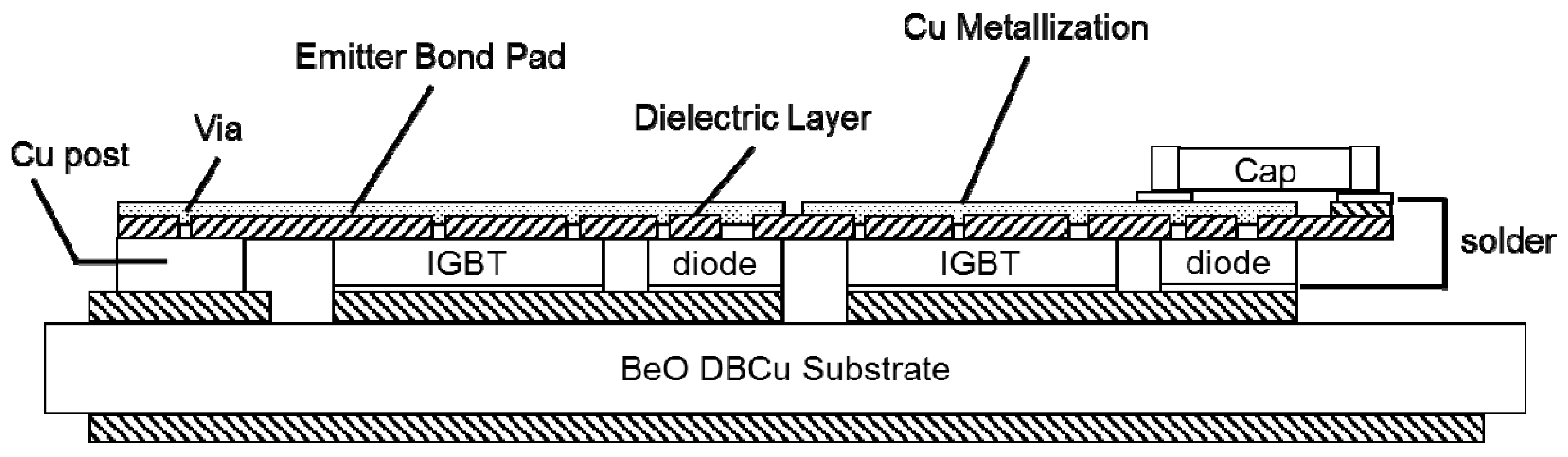
The power overlay technology proposed by General Electric in 1995 [
50] was also presented as a viable approach for wire bondless interconnections (
Figure 8). In this technology, the flexible interposer is 2 mil thick Kapton polyimide film. Vias are formed on top of the power device connections by laser ablation, and are metallized by sputtering or plating to form interconnections. Surface mount devices could be directly mounted on top of the power devices, and vertical interconnections ensured that the parasitic circuit elements were reduced significantly. This technology was capable of handling high operating voltages of up to 2400 V and a device power dissipation of up to 200 W.
The skin interconnect technology introduced by Semikron in 2011 (
Figure 9) was a major step towards both wire bond-less interconnections, as well as 3D integration [
51]. Metal traces printed on a flexible foil serve as interconnections. This foil has patterns that mate directly on top of power devices and connect to them by silver sintering technology. A 400 A, 600 V dual IGBT module using SKiN interconnections was fabricated. The thermal solution used for this module is a pin fin heat sink which is also sintered to the substrate, and is fluid cooled. This ensures high reliability performance for the module [
52] as compared to conventional solder technology. The wire bond-less SKiN module showed an average reduction of 9.68% in parasitics over a comparable wire bonded module. It was apparent from the inspection of the failure mechanisms that the joint between the flexible foil and the power device is the weak link in power cycling tests. It must be mentioned that the SKiN module survived more power cycles than any comparable state-of-the-art (SOA) module using wire bonds and bettered them by at least an order of magnitude.
In 2012, the planar interconnect technology (SiPLIT) module from Siemens was realized, which utilized copper plating over a conformally deposited insulation layer to form interconnections [
53]. The vias or openings in the insulating layer formed interconnections to the power die bond pads, and was achieved by the layer structuring process. Because of using planar interconnections, the stray inductance in these power modules showed a 50% decrease as compared to conventional wire bonded modules. The on state resistance showed a 30% decrease.
The thermal resistance offered by this packaging scheme was also lower than an aluminum wire bonded module; and the least thermal resistance was realized by using liquid cooling. From failure analysis results, it could be ascertained that the failure occurred at the junction between the copper interconnect layer and the silicon power device. The onset of failure, however, was much delayed as compared with an aluminum wire bonded module. This was attributed to the fact that copper was a relatively better match to silicon with regard to the CTE as compared to aluminum. Another reason was because this interconnect technology had a larger surface area of contact with the power die and thus the thermomechanical stresses were distributed more uniformly. This was one of the only studies that published a comprehensive reliability analysis to quantify that this approach met industry standards.
Chip-scale packaging of integrated power modules was explored by Liu et al. [
54] in 2001 as a plausible approach to improve the performance of Si IGBT power modules using 3D packaging techniques.
Figure 10a shows a photograph of the solder ball bumped devices flip-chipped onto the substrate. An 8.6% percent voltage overshoot was observed for the flip-chip module as compared with 14% overshoot of a commercially available wire bonded module (
Figure 10b). The reliability reports suggested that under thermal cycling form 0 °C to 100 °C the resistance of the solder ball interconnects did not degrade after at least 2800 cycles, and that all specimens were functionally intact after 4000 cycles.
In 2004, another integrated flip-chip module incorporating a flex-circuit was demonstrated to have 40% lower voltage overshoot and 24% lower losses as a result of implementing wire bondless techniques [
55].
Figure 11 shows the schematic of the module and the electrical benefits of the flip-chip bonding method over commercially available discrete devices. Although this is a low power module using Si devices, the benefits directly transfer to modules in the higher power range—especially since the voltage and current slew rates encountered will be more severe as the power levels rise.
In 2011, Fuji Electric [
56] proposed the use of copper pins to connect to the device bond pads instead of wire bonds(
Figure 12). The copper pins fit into the through-hole connections on the power circuit board. The copper pins were attached to the bond pad of the power device using solder. Connections to the bottom side of the die were made using copper pins as well. There were several advantages of this design apart from the obvious reduction in parasitic circuit elements: the DBC surface did not need patterning and hence the thermal resistance offered by this scheme was significantly lower than conventional methods in which the DBC must be patterned, thus eliminating conductive copper from the DBC surface and compromising thermal conductivity. The module used a rigid epoxy molding compound instead of soft silicone encapsulants normally used in wire bonded modules. It was shown in this study that rigid epoxy induced 35% less strain on the solder connections as compared to using silicones. Another interesting feature that was revealed through reliability testing was that the chief failure mode in this topology was the interfacial joint material, namely the solder. A fin heat sink was used for heat removal.
The metal post interconnected parallel plate structure (MPIPPS) module design was part of the power electronic building block (PEBB) initiative at Virginia Tech [
57,
58]. A 15 kW inverter was constructed that was capable of switching at 20 kHz, at least twice as fast as the switching speed achieved using a comparable wire bonded device.
Vertical copper posts were used to connect a driver DBC to an underlying DBC populated with power devices. The copper “posts” in this approach were separate from copper “pins” (from Fuji Electric) in that they contacted a larger area of the bond pad. This, the authors claimed provided a larger contact area for thermally induced stress distribution in the copper post. It also reduced current crowding at the junction between the interconnection post and the power device bond pad.
This study also included a detailed survey of materials that were as closely matched in CTE as physically possible in order to reduce thermal stress at the various material interfaces. This was crucial and had a direct impact on module lifetime. Inter-layers like thermal interface materials (TIMs) have also been considered. A poorly engineered interface layer drastically increases the thermal resistance of the module. Minimizing the number of interfaces from the chip to the heat sink had been proposed as a crucial aspect of the PEBB design philosophy.
One encouraging fact was revealed from the MPIPPS module—even a silicon MOSFET could be switched at a frequency of 20 kHz by adopting a wire bondless packaging scheme. This was easily double the frequency of any comparable wire bonded silicon power module of the time. Using the copper posts reduced the parasitic inductance of the interconnects to less than 2 nH, thus enabling silicon technology to be pushed to its theoretical limits.
In addition to the above power modules it is important to mention a few commercial MOSFET modules based on wire bondless technology. Although they were originally designed for low voltage silicon power MOSFETs, the design principle may serve as a base for the architecture of wire bondless SiC power modules of the future. The BGA MOSFET from Fairchild Semiconductor [
59,
60], the FlipFET, CopperStrap, and DirectFET [
61] from International Rectifier are good examples. Most of these approaches were developed to address the high parasitic source inductance and high package thermal resistance associated with the standard wire bonded SO-8 MOSFET package. Of these, the most benefits were observed for the completely wire bondless and double-side cooled DirectFET, which was reported to improve these parameters by more than 10×.
Another interesting low power silicon module was the DrMOS from Infineon. In this module, the gate drive circuit was integrated within the power module itself. This resulted in extremely low losses and high efficiencies, resulting in an increase in the allowable switching frequency. Not to mention, all this was possible at a much higher power density as a result of a highly integrated assembly. Perhaps some of the gate-driver-in-module approaches for higher power modules bear testimony to the direct adoption of the DrMOS design philosophy.
Press pack modules are among the more popular wire bondless solutions available in the market today. This solution employs mechanical pressure contacts to bond to power devices [
62,
63]. Although the target application for this is typically in the MW power range, the benefits of using this design translate directly across all power ranges. This class of modules does away with unreliable metallurgical joints like wire bonds and solder, that are prone to breaking under thermo-mechanical stresses. This type of module also has integrated short circuit protection, and is most commonly used for parallel connections between high power devices. It is not, however, an integrated power module and the gate signals must be applied externally.
Another keen insight into the packaging design problem is presented in [
64]. Material interfaces are the Achilles’ heel in power modules. The CTE mismatch between the various components in a module lead to the cracking of die attach layers and the lifting of wire bonds from the bond pads. Attachment surfaces with comparatively larger surface areas are more prone to failure by delamination.
In light of these observations, the article cites various efforts aimed at “un-packaging” where a module is stripped of unnecessary material interfaces and components in a bid to eliminate the failure modes associated with the corresponding constituents. This would directly manifest itself as an increase in reliability and module lifetime. This approach sounds ideal and gives the sense of approaching virtually monolithic electronics modules. Concepts involving embedded systems with power die, passives, and interconnections within a single interposer block follow this approach. It is also possible, if desired, to integrate thermal management within the interposer, to compensate for the comparatively lower thermal conductivities of most existing interposer materials. Is this, however, the answer to all problems?
This approach sounds ideal and theoretically solves most issues pertaining to reliability and lifetime. The cost and complexity of building such a module may be prohibitive. Integrating different components together also makes serviceability a challenge. Any kind of rework is difficult to do and may prove to be too expensive to be practical. Therefore, caution must be exercised to maintain a balance between extending the life of a module while keeping an eye on seamless serviceability in case an untimely and unforeseen failure arises.
Research in SiC power modules has redefined our conception of the performance limits of a power electronics module. Researchers continue to demonstrate prototypes capable of functioning at switching frequencies in the MHz range. SiC modules targeted toward high temperature, on the other hand, have been demonstrated to operate at temperatures above the physical limits of silicon semiconductor technology. These efforts are truly remarkable and herald in a new paradigm in the design and performance of power electronics. However, before these novel technologies are incorporated as part of systems that have a direct impact on our lives, some questions need to be answered with absolute certainty.
Let us consider the case of the high frequency SiC modules first. The information on the reliability analysis of these modules is scarce. The applications benefiting from an increased power density (as a consequence of an increased switching frequency) also require a high degree of reliability. Data centers, solar inverters for the grid, vehicular electronics—a failure to quantify reliability of these systems will have a significant impact on human life and property. It is understood that academic publications and prototypes are targeted toward demonstrating key enabling technologies. However, system reliability must be demonstrated at some level to make a technology transition possible.
As devices are switched at higher frequencies, EMI analysis is imperative. Any failures that may have occurred due to uncontrolled EMI emission must also be reported and studied. Best practices from the printed circuit board (PCB) design world may be utilized to design power modules meeting rigorous EMI specifications.
System level reliability analysis is also important for modules targeted to operate at high temperatures as well. In many studies focused on high temperature SiC modules, gate driver and control circuit boards are excluded from the elevated temperature ambient. It is well appreciated that most gate driver ICs and passives that are currently commercially available are rated for maximum operating temperatures around 125 °C. This limits researchers from demonstrating system level reliability at elevated temperatures. If the high temperature performance of the associated components around the SiC power devices are not improved, it will be difficult to justify the added costs of choosing SiC over Si IGBTs. Today commercially available Si IGBTs are rated for temperatures up to 175 °C. Hence from a strictly “high temperature” viewpoint, there needs to be some fundamental system level technological research to be able to conclusively qualify SiC as superior.
Having said that, the power density improvement offered by SiC cannot be ignored. Even if a SiC power module operates at an identical temperature level as that of a Si power module, it may theoretically operate at a much higher switching frequency and induce little or no increase in the associated switching losses. However, whether the performance gains that accompany this power density enhancement can justify the cost of using SiC technology is uncertain. There are also not many studies that relate the variation of switching losses with a variation in the junction temperature of the device. There are a few studies which suggest that it may not be possible to switch MOSFETs as fast as one might think. STMicroelectronics published an application note showing marked increase in the gate resistance with temperature [
6]. This will inhibit fast switching and may even result in higher losses in the drive circuits. Some of the above studies included in the review illustrate the advantages of using SiC technology beyond the shadow of a doubt. However, a degree of skepticism must be maintained to ascertain whether a claimed improvement in system performance would be absolutely impossible without SiC power devices. These devices are part of a larger and more complex system. While a piece-wise validation is an important first step, the need for a high level view of reliability encompassing the system as a whole cannot be disregarded.
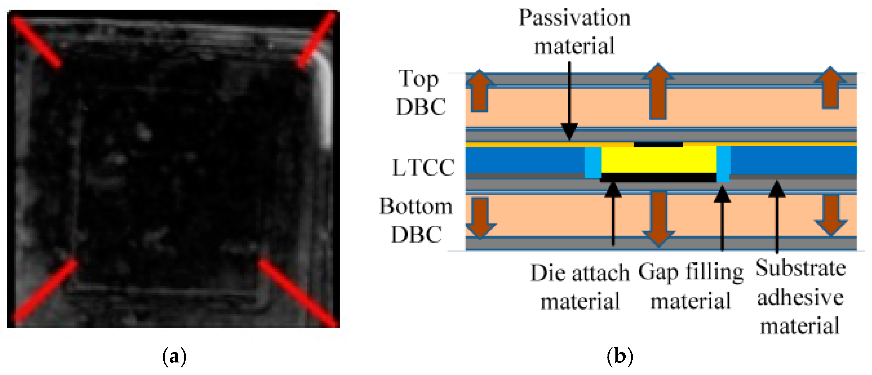
6. Present Wire Bondless Integration Efforts in Power Electronics
The realm of wire bondless SiC power MOSFET packaging, where it is capable of a much greater impact, is fairly uncharted. In 2012, researchers at the University of Arkansas developed a 6.5 kV wire bondless power module [
65]. This was followed by a similar demonstration of an LTCC-based high temperature, double-sided cooled power module in 2013 [
66]. In the 2012 version, solder was used for bonding both sides of the die to patterned DBC substrates on either side. An underfill material was used for relieving thermo-mechanical stresses. Additionally a benzocyclobutene (BCB) coating was used on the top and bottom layers to aid electrical isolation. However, after 260 thermal cycles between −40 °C and 200 °C, the solder layer was found to delaminate from the edges (
Figure 13a). The 2013 version included a rigid LTCC fixture for mechanical support instead of the underfill material (
Figure 13b). Also, sintered silver was used as the die interconnection material instead of solder owing to its superior thermo-mechanical properties. This change enabled the new version to operate at higher ambient temperatures. A double-sided cooled approach helped these novel structures maintain satisfactory operation up to 150 °C.
Additional LTCC 3D wire bondless power modules are being pursued at the University of Arkansas. One of the main reasons for using LTCC as an interposer material is the excellent CTE match it offers to SiC [
67]. The 9K7 material system from Dupont has a near perfect CTE match with SiC. Also, LTCC offers very good electrical isolation and can operate at high temperatures [
67]. This is supplemented by the fact that LTCC substrates have been the state-of-the-art for several RF and microwave engineering applications in the past, due to low dielectric losses at high frequencies. They have also been used in actuators and sensors. The LTCC material system has exhibited good reliability in these applications. All these factors work in favor of LTCC as the choice of material for an interposer in 3D SiC modules.
The 2016 3D stacked module by Dutta and Ang [
68] featured two LTCC-based standalone parallel MOSFET modules that were interconnected to form a half bridge. Each standalone module served as a switching position. The half bridge connection was facilitated by using spring loaded metallic connectors, housed in an LTCC fixture. Spring loaded interconnects have been previously used in electronics for high speed I/O with some success. The classical press pack for IGBTs has also demonstrated the viability of pressure contacts as a highly reliable interconnect approach. It will be interesting to observe the test results for high speed and high power SiC MOSFETs. The initial simulation results of the switching characteristics show promise.
The second LTCC based effort came from Zhu et al. [
69]. An LTCC interposer was used as a fixture for fuzz button interconnects. There have been several studies corroborating the benefits of using fuzz button interconnects for RF applications [
70,
71,
72,
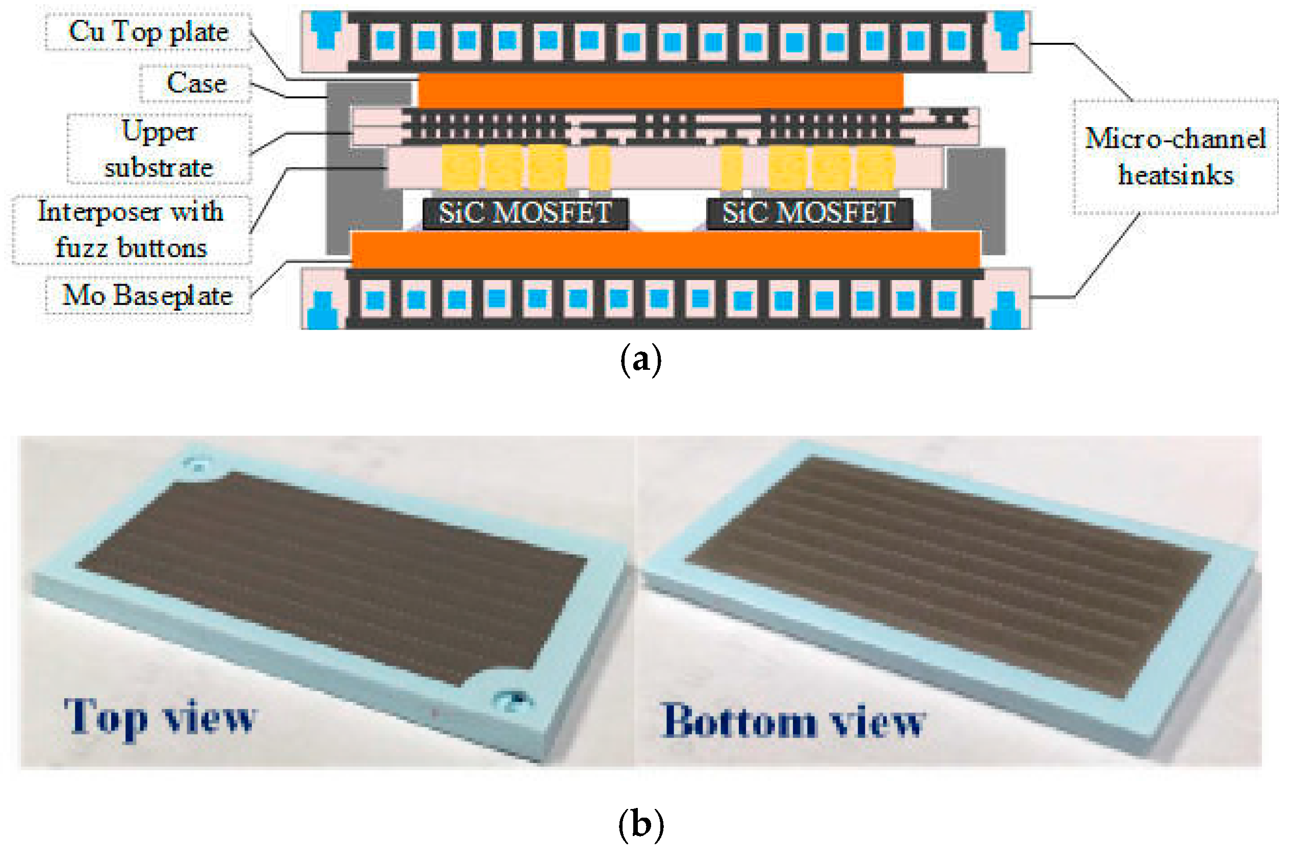
73].
Figure 14a shows a schematic of the cross section of the fuzz button press pack module. Another interesting feature of this module was the presence of an LTCC microchannel heat sink. This enabled the heat dissipation of the MOSFETs to be controlled adequately without adding significant volume to the module. Conductive traces were printed on the microchannel sink for carrying current.
Figure 14b shows a photograph of the LTCC-based heat sink. The fuzz buttons were investigated in software to show that the parasitics were contained to a minimum. Also, the thermal management was tested with a dummy heat load, and performed to expectation. The results had good correlation with the maximum temperature predicted by finite element analysis.
3D packaging of SiC modules has been embraced by APEI Inc. In some of their more recent efforts they used a stacked gate driver board atop the power stage for low inductance interconnections. However, the parasitic inductance of the wire bonds is still the limiting factor in switching performance. This fact is touched on in a 2015 publication by APEI Inc., where they demonstrated the concept of a wire bondless power module for the very first time [
74]. However, a prototype based on the design has not been released yet. The wire bondless power module used the PowerStep connector in favor of wire bonded interconnections. The connector was made of etched copper with a gold finish. Sintered silver, solder, and electrically conductive adhesives were described as possible attachment methods.
The paper presented a detailed finite element analysis of the favorable effects of adopting a wire bondless approach. Aside from the obvious reduction in loop parasitics, it was found that the thermo-mechanical stresses of the PowerStep connector were much lower than a wire bond at a junction temperature of 200 °C. This is an important feature considering the fact that one of the major benefits of SiC power devices is their ability to operate efficiently at elevated temperatures. Also, the Joule heating associated with the PowerStep connector was found to be much lower as compared with a wire bond at current loads of 100 A and above. The module was also tailored for a switching frequency of 500 kHz, enabled by the reduction in parasitics.
The modules discussed thus far in this section show great promise to offset the drawbacks associated with wire bonding. The approaches like spring pins and fuzz buttons have already been proven to be beneficial in high speed electronic circuits in the past. With careful design considerations, these benefits should translate to high power modules as well. The success of press pack modules bears testimony to the success of this design philosophy. However, it is important to note that the described approaches are power modules. They must still be routed to a gate driver board to operate in the field. This implies that the parasitic gate inductance of the module is not the sole force to reckon with. The connection to and from the gate driver board, and the board parasitics will also play a key role in determining the behavior of the switching transients and associated EMI behavior. This fact has been highlighted in some of the integrated power modules that have been presented in this paper. Implementing the gate driver “on board” or “in module” was the driving factor behind their success.
7. Future Directions
The future of SiC power modules could be “the best of both worlds”—by implementing wire bondless technology in an integrated power module. Efforts are underway at the National Science Foundation (NSF) Center for Power Optimization of Electro-Thermal Systems (POETS) Engineering Research Center (ERC) to deliver the SiC power module of the future based on this concept. This section will summarize some of the integrated SiC module design concepts proposed by the POETS ERC this year.
In 2016, the concept for an LTCC-based integrated wire bondless power module (IWPM) was put forth [
75]. A simple schematic showing the cross section of the proposed module is shown in
Figure 15. The interposer was envisioned as a shallow container made of Dupont 9K7 LTCC material. The material of the interposer was chosen for reasons stated earlier. Power devices were mounted on the bottom side of the interposer, such that the gate and source pads of the SiC power devices contacted the interposer surface. The top side contacts of commercially available SiC power devices in bare die form are made of aluminum, and this was proposed to be converted to a Ni/Ag finish by using an electro-less plating process. The choice of material for the flip-chip die attach material was sintered silver. The bottom side of the power devices were proposed to be connected by an electrically conductive metal foil bonded by sintered silver. The metal foil would, in turn, be bonded to a designated pad on the interposer to complete the current path.
The top side of the interposer would house the gate drive circuits for the power devices on the bottom tier. The connection from the output of the gate driver chip to the gate pad of the MOSFET was achieved by a through LTCC via, filled completely with conductive paste and cured. The module showed very low thermo-mechanical stresses at a nominal junction temperature 80 °C.
A follow up study in 2016 by Seal et al. [
76] demonstrated a single integrated switch module based on the design principle of the integrated wire bondless power module (IWPM).
Figure 16a shows a rendering of the proposed module with the encapsulation removed, showing the gate driver, isolator, and passive devices on the top layer. The bare die SiC MOSFET was on the bottom layer, as with the IWPM. Simulations of a double pulse test of the module at a high slew rate showed a drastic reduction the levels of ringing and overshoot associated with the module as compared with a conventional wire bonded module (
Figure 16b,c).
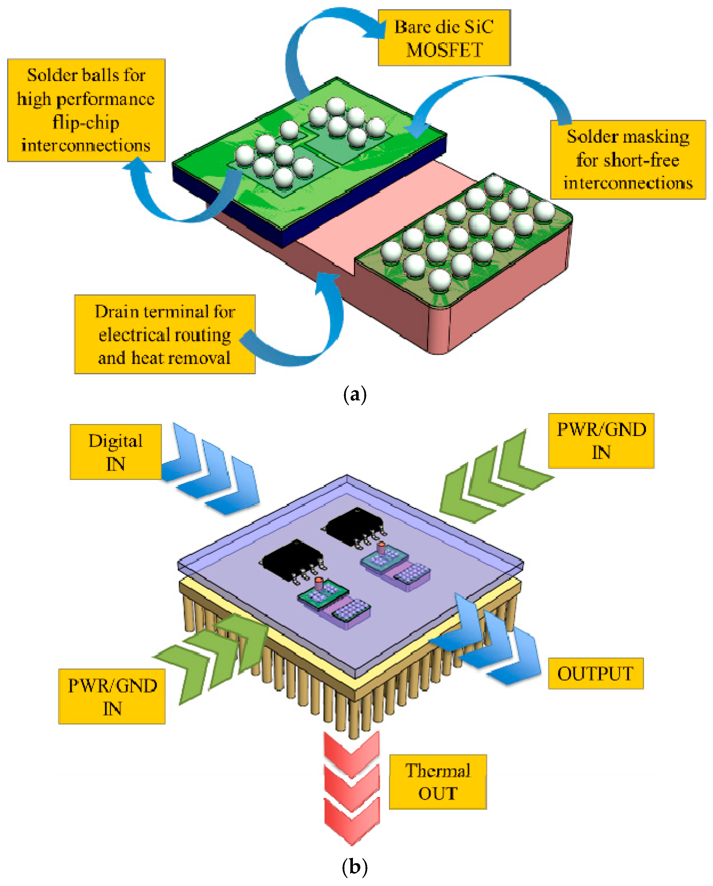
Under a power dissipation of 100 W, the proposed module reached a maximum junction temperature of 140 °C, thus meeting the 150 °C maximum rating of the device itself. Under this thermal load, the mechanical stress on the flip-chip contacts were found to be less than half that of a conventional wire bonded MOSFET assembly. However, the stress was found to be concentrated at the edge of the flip chip contact. This would make the die attach layer susceptible to cracking at the edges within a few hundred thermal cycles. Moreover, using sintered silver for flip-chip bonding on an LTCC interposer may introduce considerable process cost and complexity. Also, the electrical conductivity of sintered thick film conductors on LTCC is not as high as copper. For high current modules, this was an important issue to consider because it may introduce undesirable voltage drops and cause unwanted hot spots in the interposer. To address these concerns, the concept of the flip-chip MOSFET package was developed.
A fourth 3D SiC module concept was proposed by researchers at the University of Arkansas in 2016 [
77]. The first step in building the module was to reconfigure a commercially available bare die MOSFET into a flip-chip capable package. A chip-scale MOSFET was developed, a schematic of the part is shown in
Figure 17a. A commercially available bare die MOSFET was attached to a metallic drain connector. The material of the drain connector was chosen to be copper for cost considerations, but a composite material like CuMo or AlSiC with a better CTE match to SiC may be used for greater reliability. The assembly was solder masked and solder ball bumped to produce the flip-chip capable chip scale package.
Figure 17b shows the schematic of a power module incorporating these flip-chip SiC MOSFETs. The philosophy behind this approach was similar to the IWPM, but this method employed several known-good design practices to improve the manufacturability, repeatability, and serviceability of the integrated power module.
The drain connector has the dual purpose of serving as a low thermal resistance path to the heat sink. Another noticeable feature of this approach was the absence of a power substrate. In a way, this approach is similar in principle to attaching the die directly on the baseplate. This has the benefit of decreasing both the thermal path and the number of interfaces in a power module.
A solder ball array was used in the module instead of a flat soldered/sintered interface. As mentioned earlier, a flat bond line showed an accumulation of thermo-mechanical stress along the edges—thus making the bond susceptible to premature cracking under thermal stress. Solder balls have been used in BGA interconnection over the past several decades as a highly dense and reliable form of interconnection. This packaging technique exploited the best characteristics that BGA technology had to offer. One of the concerns with using a flat bond line was that the die may be marginally skewed after the reflow/sintering process. This slant would facilitate cracking from the narrow edge under repeated thermal stress. Solder balls have a tendency to reflow and self-planarize [
78]. They also have the property of self-aligning due to surface tension. Even if the end user does not place the part perfectly accurately during flip-chip bonding, the surface tension of molten solder has a tendency to “pull” the part into the right location [
79].
BGAs also have known good reliability as discussed in an earlier section. A study by Lin and Luo showed that SnAg flip chip solder bumps survived more than 3000 thermal cycles, even when mounted on inexpensive FR4 substrates [
80]. Some studies also showed a strong correlation between interconnect parasitic inductance and EMI emissions [
81,
82]. BGA technology has been known for having much less parasitic inductance as compared with wire bonds, and is thus expected to produce less EMI. This was expected to be a highly desirable feature in a power module intended to operate at high voltage/current slew rates.
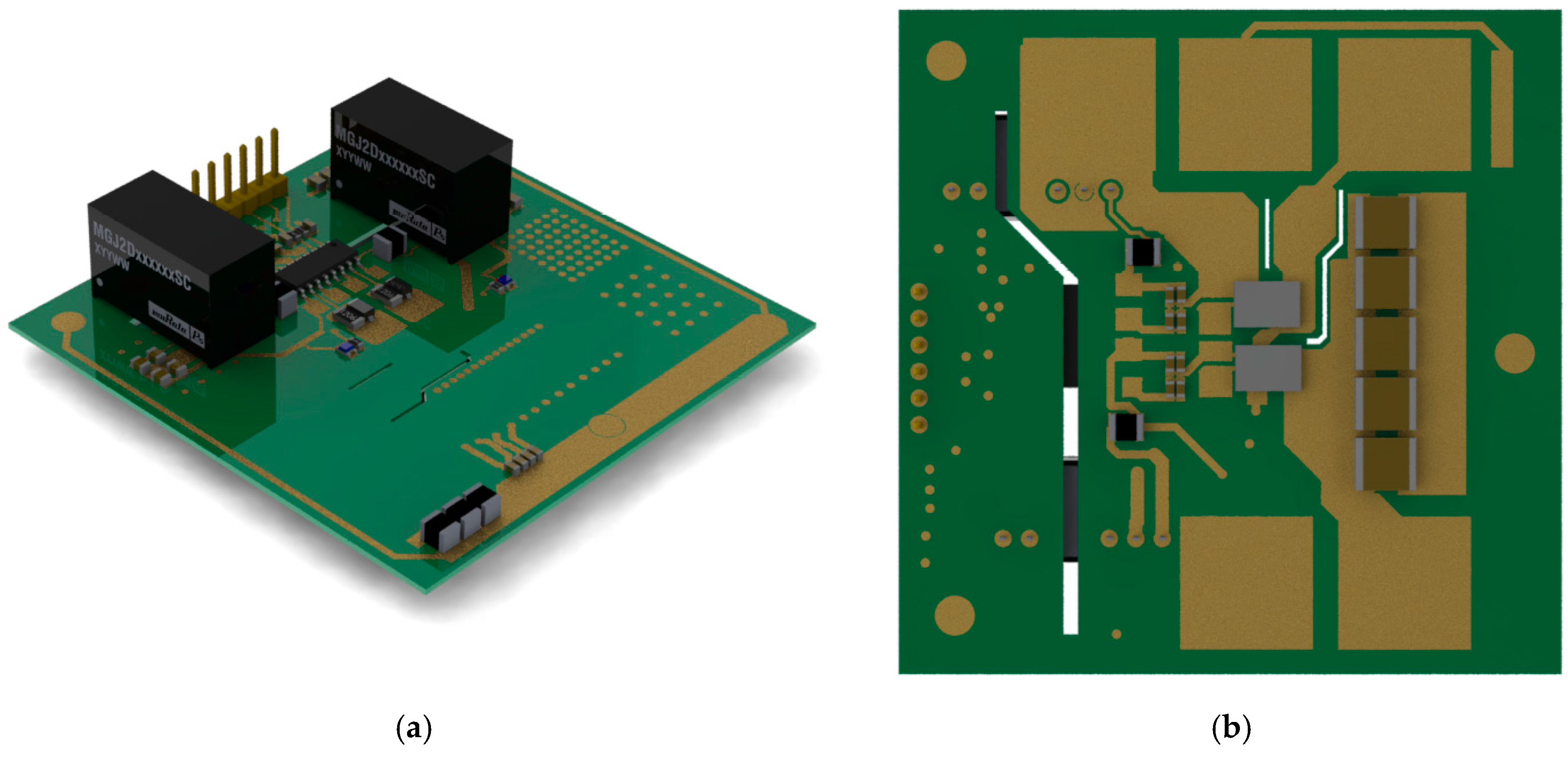
Future work on this module will include the assembly of the chip-scale packaged MOSFETs on a PCB with an integrated gate driver and passive circuitry (
Figure 18). The circuit topology is that of a half bridge employing two 1200 V MOSFETs from ROHM Semiconductor. The top side of the PCB houses the gate driver chip and power supplies, along with the other passives necessary for the gate drive to function.
A few capacitors and inductors for inductively isolating the heat sink are also mounted on the top side. This will help in mitigating EMI by suppressing any injected current spikes that may propagate through the heat sink because of the parasitic capacitance between the drain connector and the heat sink [
83]. The bottom side of the PCB contains the two chip-scale MOSFETs serving as the two switch positions of the half bridge. EMI suppression capacitors are also mounted in the bottom side. Mounting the DC link capacitor close to the MOSFETs in this fashion proved to be the most effective in EMI spike suppression according to some studies using the GaN material system [
84].
8. Conclusions
SiC devices are fast becoming the semiconductor device of choice in most advanced applications. The demand will only continue to increase as the world becomes more electrified. Having access to power converters that fit within the palm of our hands may give rise to innovations that are yet to be imagined.
The enormous potential that SiC offers as a semiconductor material has not been explored completely. We tend to use performance limiting packaging technologies and restrain the full benefits of SiC technology. Researchers had already encountered the glass ceiling of package performance with silicon devices in the past. Many examples in this paper bear testimony to the adoption of unconventional silicon power packaging solutions in a bid to extricate that much more in terms of thermal and electrical performance. SiC packaging research needs to progress along the same line.
The bottlenecks in state-of-the-art SiC power modules needs to be identified. Investigations need to be conducted to ascertain the part/parts of the package giving rise to these performance limits. This must be followed by innovative redesign in the appropriate direction to push SiC modules further. Interconnect technology is one of the major limiting factors plaguing SiC modules of the present. Wire bonding offers too much parasitic inductance to be able to run SiC power devices at the frequencies it is capable of. Ringing and overshoots due to parasitic loop inductance are only a part of the problem—EMI emissions are a worse consequence which may lead to a catastrophic failure due to a false switching event. Many power electronics research groups around the globe are realizing this, and a there has been a noticeable push in the direction of low inductance SiC package designs in the recent past.
Efforts at the University of Arkansas are focused on providing high-performance alternatives to wire bonding. Approaches involving spring pin interconnects, fixtured fuzz buttons, and solder ball interconnects have proven to be winning choices in high speed, low power electronics applications in the past. The endeavor is to re-engineer these methods to render them applicable to SiC power modules at all power levels. Some of the recent efforts in this direction have been described, and these will help lay the bedrock of a better understanding of these interconnect technologies as it applies to SiC packaging. Evaluating and weighing these approaches against one another will help establish new standards for packaging technologies suited to the needs of a particular application.
Wire bondless integration will also introduce possibilities of double-sided cooling and 3D integration, once again depending on what the end application would benefit the most from. Compact integration coupled with faster switching frequencies will enable an unprecedented power density. In a rapidly growing electronics market, less is more. Smaller and lighter power electronics may completely change the way we perceive the world.


