Abstract
A multiscale model that enables quantitative understanding and prediction of the size effect on the scattering properties of micro- and nanostructures is crucial for the design of light-emitting diode (LED) surface textures optimized for high light extraction efficiency (LEE). In this paper, a hybrid process for combining full-wave finite-difference time-domain simulation and a ray-tracing technique based on a bidirectional scattering distribution function model is proposed. We apply this method to study the influence of different pattern sizes of a patterned sapphire substrate on GaN-based LED light extraction from the micro-scale to the nano-scale. The results show that near-wavelength–scale patterns with strong diffraction are not expected to enhance the LEE. By contrast, micro-scale patterns with optical diffusion behavior have the highest LEE at a specific aspect ratio, and subwavelength-scale patterns that have antireflection properties show a marked enhancement of the LEE for a wide range of aspect ratios.
1. Introduction
Over the past 10 years, numerous studies in the field of light-emitting diode (LED) solid-state lighting have focused on how to improve luminous efficacy. Light extraction efficiency (LEE) has played an important role in this research regarding the development of highly efficient LEDs [1,2]. The LEE of a typical LED is generally low, mainly because of the large refractive index difference between the LED material and the surrounding environment. Most of the photons are completely internally reflected and are thus trapped inside the LED. Therefore, to substantially enhance the LEE of the LED, various textured structures have been proposed to avoid the occurrence of total internal reflection, including rough surfaces, patterned substrates, diffraction gratings, and photonic crystals. Experiments have proven that these textured structures can enhance the LEE, and that they all appear to function in the same manner, namely by using light scattering effects to increase the probability of photon escape [3,4,5,6,7,8,9]. However, because research is typically conducted using trial and error during the manufacturing process, it is not easy to obtain the optimal structural parameters, nor is it possible to further understand the impact of the light scattering factor on the LEE. A set of fast and precise optical models for analyzing the LEE would enable the results of the experiments to be analyzed through optical simulations and then be used in the manufacture of devices, thereby reducing unnecessary trial and error and cost while increasing efficiency.
The Monte Carlo ray-tracing method is a widely used numerical scheme for simulating and designing optical and illumination systems. The method has also successfully been applied to the analysis of the LEE of LEDs with different light extraction structures [10,11]. In 1974, Joyce et al. [12] presented the concept of the “random particle” to analyze the LEE of LEDs. In 1995, Ting and McGill [13] used the Monte Carlo ray-tracing method to simulate the properties of the light source of the LED based on the randomness of the photons. The advantage of this method is that it can effectively simulate the light-emission behavior involved in the spontaneous emission of photons in the active region of the LED. With the ray-tracing algorithm, the trajectory of each photon inside the LED is calculated and the LEE of the LED is analyzed. However, because the simulated textured structures’ dimensions are smaller than the simulated wavelength of light, the effects of diffraction and electromagnetic wave propagation cannot be neglected and the ray-tracing method has difficulty representing them. Thus, some literature has suggested the use of a rigorous coupled wave analysis (RCWA) or finite-difference time-domain (FDTD) method to simulate the impact of the wavelength- and subwavelength-scale structures on the LEE of LEDs [14,15,16].
While successful in many applications of LED light extraction, these wave-based methods also exhibit limitations, particularly with respect to simulating the multiple reflection of the light inside the LED. Moreover, to greatly reduce the computing time, because the simulation domain is limited to a small 3D range or a 2D domain, it ignores the impact of the boundary or skew ray effect on the LEE [17,18]. Additionally, a complex and lengthy modeling process simulating the random properties of emitted photons is required for the behavior of the spontaneous emission to be represented by the RCWA or FDTD methods [19]. To date, no universal method has been developed that can resolve all the textured structures from the nano-scale to the micro-scale, making it impossible to compare studies with different simulation methods to determine which scale (e.g., size, spacing, height) of textured structures is the most suitable for analyzing LEE.
To overcome the limitations of the ray-based and wave-based methods, we combine the characteristics of the two in a simple but effective simulation process for analyzing LED light extraction, and refer to this method as the “hybrid approach”. Using the hybrid approach, we are able to successfully resolve the issue of the ray-tracing approach being unable to simulate the nano-scale structure, while also avoiding the restriction of the full-wave method, which is unable to consider the overall LEE.
2. Preliminary Study
We measured the scattering light for two textured structures on sapphire substrates of different dimensions. As shown in Figure 1, these two textured structures are known as “patterned sapphire substrates” (PSSs). Their distribution is in a periodic hexagonal arrangement. The structure in Figure 1a was created using inductively coupled plasma dry etching. This structure is hemispherical, with a bottom width of 2.5 μm and a height of 1.5 μm. The distance between the two centers is 3.0 μm (i.e., the shortest distance between the structures is 0.5 μm). The structure in Figure 1b was also created with dry etching, and its shape is similar to that of a bullet. The bottom width is 0.9 μm, the height is 1.5 μm, and the distance between the two centers is 1.0 μm (i.e., the shortest distance between the structures is 0.1 μm).
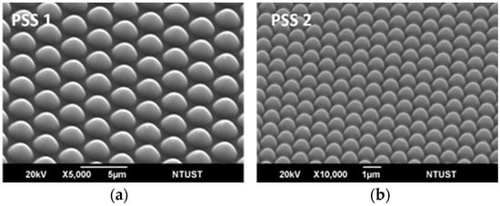
Figure 1.
PSS structures (scanning electron microscopy) at two scales: (a) PSS 1: 2.5 μm width, 1.5 μm height and 3.0 μm pitch; (b) PSS 2: 0.9 μm width, 1.5 μm height and 1.0 μm pitch.
Figure 2 shows the forward and backward light scattering patterns for blue light of a 450 nm wavelength incident at 30° from the structure surface (the other surface is polished). An IS-SATM (Radiant Vision Systems, Redmond, WA, USA) was used for the measurement. The figure shows that the PSS structure exhibits strong diffraction for both forward transmitted and backward reflected light, and that the diffraction angles of the light for the PSS structure are different to a certain extent. We further measured the total transmittance and reflectivity of the incident light at different angles, with the results shown in Figure 3. Different diffraction characteristics appear to cause large changes in the transmittance and reflectivity of the light. For the first PSS structure, when the angle of the incident light was larger, the transmittance dropped and the reflectivity increased, and the transmittance (30%) was poorest when the angle of the incident light was at 60°. For the second PSS structure, when the incident angle was less than 30°, the transmittance and reflectivity followed the same trends as those of the first PSS, although for incident light greater than 30°, the transmittance and reflectance fell within a range of 45% to 55%.
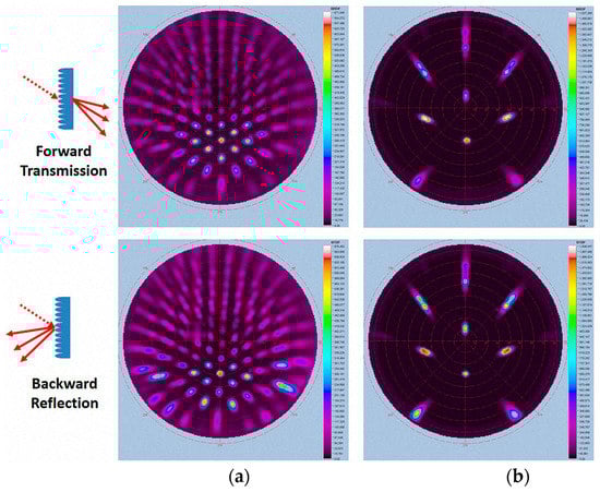
Figure 2.
Forward and backward light scattering patterns for a light incident at 30° from the structure surface: (a) PSS 1 and (b) PSS 2.
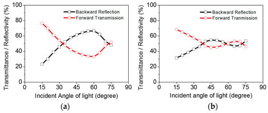
Figure 3.
Total transmittance and reflectivity of incident light at different incident angles: (a) PSS 1 and (b) PSS 2.
These observations raise the questions of which light distribution related to the scattering or diffraction of the light caused by these textured structures would more greatly benefit LED light extraction, and what phenomenon is caused by the structures of the various dimensions of the microstructure, submicron structure, and nanostructure [20,21,22]. These are the main focuses of this paper. We hope to clarify and present solutions to these questions through the establishment of the hybrid simulation approach.
3. Simulation Method
To investigate the influence of the multiscale textured structures on the LED light extraction performance, we use a GaN-based flip-chip LED with a PSS as an example. The LED structure used for the simulation consists of a highly reflective backside mirror, LED epitaxial layers (P-GaN/MQW/N-GaN), and a two-dimensional pyramid-textured PSS with a periodic array structure, as shown in Figure 4. The pyramid structure has a square base with a size of 0.1, 0.5, 1.0, or 4 μm, which ranges from the nano- to the micro-scale. The arrangement is a compact square array and the array pitch is equal to the size of the pyramid structure. Moreover, to unify the parameters of the geometry of textured structures with any scale, we use the aspect ratio, which is defined as the ratio of the structure height to the structure width. Because the base of the structure is fixed, the structure depth and tile angle can be determined simultaneously. The range of the aspect ratio in the simulation was set from 0.1 to 3.0, which means that the scale of the structure depth from micro to nano was also considered.
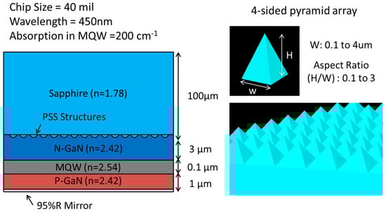
Figure 4.
Structure of the nitride-based blue LED with a PSS in the simulation.
There are three main steps to combining the FDTD and ray-tracing methods to simulate the LEE of the LED: First, the full-wave FDTD simulation is used for the computation and collection of the bidirectional light scattering field (BLSF) data when the light strikes the region surrounding the textured structure. An equivalent light scattering model is then necessary to replace the real textured structure built into the LED geometry and luminosity model. Finally, through Monte Carlo ray tracing, the LEE can be determined exactly for either the micro- or nano-scale textured structure. Accordingly, establishing a suitable and accurate BLSF as a link between these two analytic methods is critical.
In the FDTD part of the simulation procedure, the BLSF of textured structures between the sapphire and n-GaN layer is simulated in detail. This can be achieved by individually solving the incident plane-wave scattering from the structure surface with the wavelength, the propagation direction, and the state of polarization. In this paper, the free-space emission wavelength is assumed to be λ = 450 nm, and the propagation direction is specified by the polar angle and the azimuth angle . To accurately describe the scattering behavior of the textured structure, it is therefore necessary to correctly quantify its response for all plane-wave propagation directions. Because we consider the case of a periodic pyramid structure with square symmetry, the polar angles can be set only in the interval and the azimuth angle is considered only at and for both transverse electric (TE) and transverse magnetic (TM) polarizations. For simplicity, the scattering data are averaged over two azimuth angles and two polarizations with respect to the polar angle, and therefore an isotropic BLSF, which depends on the incident polar angle and on the scattering angles , is obtained. We tested the simplified procedure through simulations and determined that different azimuth angles have only a negligible impact on the calculations of the LEE if the periodic structure is highly symmetrical. Furthermore, in the case of an LED with a PSS, two BLSFs are required to fully characterize the interaction of light with the structure surface. This is because, in general, the emitted light from multiple quantum wells is incident from the front side of the N-GaN layer on the structure surface, although some light may be reflected to the structure surface on the sapphire backside, resulting from total internal reflection on the other interface. Therefore, the two BLSFs represent bidirectional transmission and reflection in two opposite orientations, namely front transmission (FT), front reflection (FR), back transmission (BT), and back reflection (BR), as shown in Figure 5. According to the preceding explanation, the total number of BLSF data in FDTD plane-wave simulations for each textured structure is .
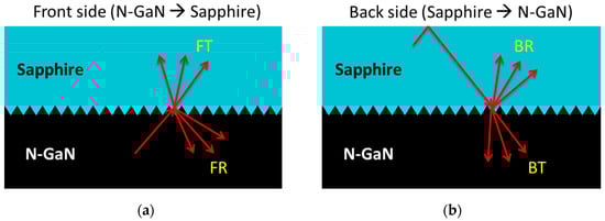
Figure 5.
Bidirectional transmission (FT, BT) and reflection (FR, BR) in two opposite orientations: (a) Light incident from N-GaN into sapphire; (b) Light reflect from sapphire and into N-GaN.
Figure 6 shows that the light wave propagates from N-GaN to the sapphire in the FDTD computational domain. The Bloch periodic boundary condition is applied to all four sides normal to the plane of the structure surface, and a perfectly matched layer-absorbing boundary is assumed at the top and bottom planes. As expected, the near-field scattered light of the reflection and transmission at a distance of 1.0–1.5 λ from the structure surface is recorded by detectors of FT and FR, respectively. The other two detectors, monitoring BT and BR, perform the same task but with different input orientations. A near- to far-field transformation is then applied to obtain the light scattering angular distribution in the far-field region. This transformation is routinely used in the FDTD method for calculating electromagnetic fields far from the computational domain boundary [23]. The numerical simulation software FDTD Solutions (Lumerical, Vancouver, BC, Canada) was employed to collect information on the simulated far-field scattering for transmission and reflection under different input conditions.

Figure 6.
Illustration of the FDTD computational domain.
After finishing the FDTD simulation, we required a universal scatter model that most accurately describes the wide range of surface scattering properties for accelerating the ray-tracing simulation. To address this concern, we use the bidirectional scattering distribution function (BSDF) with tabular data, rather than the analytic function, which is applicable to diffraction patterns from a nanostructured surface. “BSDF” is a general term that includes both bidirectional transmittance functions and bidirectional reflectance functions. In the simplest terms, the BSDF is the ratio of the luminance in a specific direction to the illuminance from a specific direction. The following equation defines the BSDF as a function of both the incoming illuminance per incidence angle and the outgoing luminance per outgoing angle [24],
The tabular BSDF model for each structure surface consists of four matrices that convert a scattering Poynting vector intensity distribution to scalar 3D isotropic BSDF data. Each matrix has data for 91 polar and 361 azimuth angles of the outgoing light direction for 91 incident light directions; therefore, the total number of data for a structure surface is . Hence, for comparison with general BSDF measurements, the present BSDF generation method from the FDTD simulation can easily provide a dense and accurate sampling of the BSDF data for samples with differently scaled textured structures.
Finally, three-dimensional Monte Carlo simulation was performed using LightTools software (Synopsys, Mountain View, CA, USA) to study the impact of structure texturing on the LED light extraction. The chip size used in the simulation was mil2. The refractive index, absorption coefficient, and other material parameters are described in Figure 4. Only the textured structure was replaced with that of the four equivalent BSDF models. Using the Monte Carlo method, the distribution and direction of light rays are generated randomly within the active region. In general, for each ray, the trajectory and energy are determined by Snell’s law, the Fresnel reflection, and the material absorption. However, when a ray impinges on the interface of the virtual structure surface, the ray is split into more rays, including reflected scattered rays and transmitted scattered rays, which are represented by ray data within the bidirectional reflectance distribution function (BRDF) model, as shown in Figure 7. Accordingly, whether the textured structure is in the micro- or nano-scale range, the LEE of the LED can be effectively evaluated and analyzed using the hybrid method.
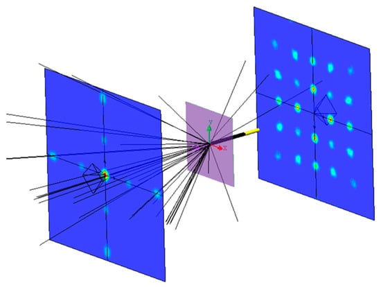
Figure 7.
Schematic of the diffraction BSDF model for ray-tracing simulation.
4. Results and Discussion
Based on the FDTD method, the light scattering far-field angular distribution of FT and FR resulting from the interaction of textured structures of various scales when the aspect ratio is equal to one at different incident angles is shown in Figure 8 and Figure 9, respectively. Similarly, the simulation results for the behavior of BT and BR have the same variation trend. The figure illustrates that the main difference between various scattering effects lies in the fraction of the emission wavelength (450 nm) at different structure sizes. The feature size of the textured structure set in the simulation covers a wavelength scale range of 0.2 λ to 9 λ. For 9λ, which is a micro-scale structure, we observed that the optical diffusion effect of the reflected field was stronger than that of the transmitted field. When the structure size was reduced to the near-wavelength scales 1 λ and 2 λ, for both the transmitted and reflected fields, the diffraction grating effect became dominant and therefore the light scattering could no longer be described by the refraction process. If we further refined the structure size to the subwavelength scale (i.e., 0.2 λ), the wide-angle antireflection, also called transparent enhancement, effect was observed [25]. From the preceding conclusion, we can identify the differences in the scattering caused by various scales of the microstructures. We further simulated the LEE of the LED with the hybrid method and summarized the impact of the effects of the scattering on the LEE. We also analyzed the aspect ratio parameter of these microstructures of various scales as an example to identify the optimal LEE using the hybrid method.
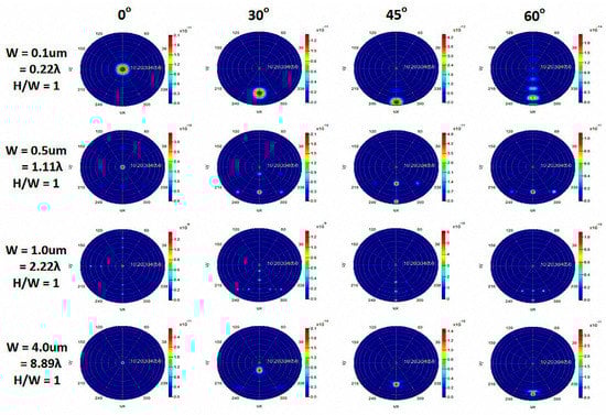
Figure 8.
Light scattering far-field angular distribution of FT (both images use a logarithmic scale for the intensity of the false-color plot).
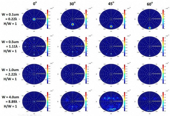
Figure 9.
Light scattering far-field angular distribution of FR (both images use a logarithmic scale for the intensity of the false-color plot).
Figure 10 depicts a plot of the calculated LEE of the bare LED chip as a function of the aspect ratio for different structure sizes. For the 9 λ micro-scale structure, the results show that the LEE has a strong dependence on changes in the aspect ratio. As the aspect ratio increases from 0 to 1, the LEE increases, and the LEE reaches a maximum when the aspect ratio approaches unity. When the aspect ratio is greater than unity, the LEE begins to decline. When the textured structure size is one to two times the wavelength scale (i.e., 1 λ and 2 λ), the LEE trend for the different aspect ratios is similar to that of the preceding case for the 9 λ micro-scale structure. However, for these near-wavelength structures, their overall LEE is lower than that of the micro-scale structure, especially when the structure size is close to the emission wavelength. These observations reveal that the LEE is suppressed in the presence of a strong diffraction effect, which can substantially inhibit the LEE enhancement from the near-wavelength structures. For the 0.2 λ subwavelength structure, the LEE shows less dependence on the aspect ratio of the structure, and the LEE is effectively increased because of the antireflection in the wide-angle range; this causes the light extraction enhancement revealed by our simulation results. Comparing the structure scales in the micro to nano range indicates that a nanotextured structure has the highest LEE in a bare chip.
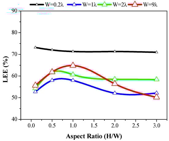
Figure 10.
Calculated LEE of the bare LED chip (i.e., the environment is set to air, n = 1).
Next, the LEE of a packaged LED was analyzed, yielding the results shown in Figure 11. We adopted hemisphere lens packaging. The diameter of the hemisphere was set at 10 times the size of the LED die. The purpose of this was to eliminate the effect of total internal reflection caused by the packaging. The figure reveals that the LEE trend of the packaged LED was similar to that of a bare chip, and the overall LEE of all the textured structures was enhanced because of the change in the refractive index. Regarding the bare chip, the near-wavelength structures have the lowest LEE, and the subwavelength structure maintains a higher LEE at all aspect ratios. However, the LEE of the micro-scale structure is higher than that of the near-wavelength structures when the aspect ratio is between 0.3 and 1.4. From [26,27], we can infer that the micro-scale structure results in the backward scattering of light. The scattered light that is reflected back changes the path, thus increasing the likelihood of the light entering the light emission cone, especially in packaged LEDs. That is, if the light cannot be emitted the first time, there is still a chance that the reflected light can be extracted after it changes course and is reflected again at the bottom. Such cycles facilitate achieving a high LEE. This means that the reflectivity of the bottom of the LED is key to the enhancement of the LEE.
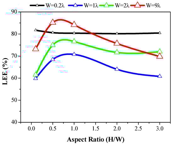
Figure 11.
Calculated LEE of the packaged LED (i.e., the environment is set to silicone, n = 1.5).
To verify the accuracy of our proposed method, we used a pure ray-tracing method to simulate a 9 λ micro-scale structure for comparison. The usefulness of the ray-tracing method at the micro-scale has been established by the aforementioned studies. As shown in Figure 12, according to the simulation results, both methods have the same trend, partially demonstrating the feasibility of our proposed method as a multiscale structure simulation technique.
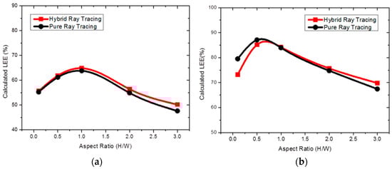
Figure 12.
Hybrid vs. pure ray-tracing method for microscale structures: (a) bare LED chip and (b) packaged LED.
5. Conclusions
The FDTD and ray-tracing methods were combined using the BSDF model to analyze the LEE for GaN-based flip-chip LEDs with a PSS using a pyramid-textured structure ranging from the micro- to the nano-scale. This method enables comparing and evaluating the LED light extraction mechanism across all scales of the textured structure. The results indicate that the light scattering properties caused by differently textured structure sizes are critical for optimizing the LEE. Marked enhancement of the LEE is observed using micro-scale or subwavelength-scale structures, with the subwavelength structure showing more enhancement than the micro-scale structure for a wide range of aspect ratios. However, the near-wavelength structures, which generated strong diffraction effects, should be avoided, because they cannot improve the LEE effectively. Further optimization work could be performed using this hybrid method to enhance the LEE by simultaneously analyzing more multiscale textured structures with various shapes, thicknesses, and pitches.
Acknowledgments
This study was sponsored by the Ministry of Science and Technology (MOST) of the Republic of China with the contract number 103-ET-E-011-005-ET.
Author Contributions
Tsung-Xian Lee conceived and designed the simulation methods and experiments, as well as analyzed the data and wrote the paper. Ching-Chia Chou implemented the measurement.
Conflicts of Interest
The authors declare no conflict of interest.
References
- Zhmakin, A.I. Enhancement of light extraction from light emitting diodes. Phys. Rep. 2011, 498, 189–241. [Google Scholar] [CrossRef]
- Gan, J.; Ramakrishnan, S.; Yeoh, F.Y. A review on improvement of LED light extraction efficiency through a micro repeating structure. Rev. Adv. Mater. Sci. 2015, 42, 92–101. [Google Scholar]
- Schnitzer, I.; Yablonovitch, E.; Caneau, C.; Gmitter, T.J.; Scherer, A. 30% External quantum efficiency from surface textured, thin-film light-emitting diodes. Appl. Phys. Lett. 1993, 63, 2174–2176. [Google Scholar] [CrossRef]
- Fujii, T.; Gao, Y.; Sharma, R.; Hu, E.L.; DenBaars, S.P.; Nakamura, S. Increase in the extraction efficiency of GaN-based light-emitting diodes via surface roughening. Appl. Phys. Lett. 2004, 84, 855–857. [Google Scholar] [CrossRef]
- Dang, S.H.; Lia, C.X.; Li, T.B.; Jia, W.; Han, P.D.; Xu, B.S. Light-extraction enhancement and directional emission control of GaN-based LED with transmission grating. Optik 2014, 125, 3623–3627. [Google Scholar] [CrossRef]
- Trieu, S.; Jin, X.; Ellaboudy, A.; Zhang, B.; Kang, X.N.; Zhang, G.Y.; Chang, X.; Wei, W.; Jian, S.Y.; Xing, F.X. Top transmission grating GaN LED simulations for light extraction improvement. Proc. SPIE 2011, 7933, 79331Y. [Google Scholar]
- Wu, G.M.; Yen, C.C.; Chien, H.W.; Lu, H.C.; Chang, T.W.; Nee, T.E. Effects of nano-structured photonic crystals on light extraction enhancement of nitride light-emitting diodes. Thin Solid Films 2011, 519, 5074–5077. [Google Scholar] [CrossRef]
- Yoon, K.M.; Yang, K.Y.; Byeon, K.J.; Lee, H. Enhancement of light extraction in GaN based LED structures using TiO2 nano-structures. Solid State Electron. 2010, 54, 484–487. [Google Scholar] [CrossRef]
- Che, Z.; Zhang, J.; Yu, X.; Xie, M.; Yu, J.; Lu, H.; Luo, Y.; Guan, H.; Chen, Z. Optimized double-sided pattern design on a patterned sapphire substrate for flip-chip GaN-based light-emitting diodes. Opt. Eng. 2015, 54, 115108. [Google Scholar] [CrossRef]
- Lee, T.X.; Gao, K.F.; Chien, W.T.; Sun, C.C. Light extraction analysis of GaN-based light-emitting diodes with surface texture and/or patterned substrate. Opt. Express 2007, 15, 6670–6676. [Google Scholar] [CrossRef] [PubMed]
- Pan, J.W.; Wang, C.S. Light extraction efficiency of GaN-based LED with pyramid texture by using ray path analysis. Opt. Express 2012, 20, A630–A640. [Google Scholar] [CrossRef] [PubMed]
- Joyce, W.B.; Bachrach, R.Z.; Dixon, R.W.; Sealer, D.A. Geometrical properties of random particles and the extraction of photons from electroluminescent diodes. J. Appl. Phys. 1974, 45, 2229–2253. [Google Scholar]
- Ting, Z.Y.; McGill, C. Monte Carlo simulation of light-emitting diode light-extraction characteristics. Opt. Eng. 1995, 34, 3545–3553. [Google Scholar] [CrossRef]
- Shen, X.X.; Ren, Y.Z.; Dong, G.Y.; Wang, X.Z.; Zhou, Z.W. Optimization design of holographic photonic crystal for improved light extraction efficiency of GaN LED. Superlattices Microstruct. 2013, 64, 303–310. [Google Scholar] [CrossRef]
- Behill, A.; Aleman, G.; Jin, X.; Kang, X.N.; Zhang, G.Y. Study of grating layer location of a GaN nano-grated led for improvement of transmission efficiency. Proc. SPIE 2014, 9003, 90031J. [Google Scholar]
- Lee, G.J.; Song, Y.M. Theoretical analysis and experiment of subwavelength structure-integrated red AlGaInP light-emitting diodes for uniform field distribution and enhanced light extraction efficiency. AIP Adv. 2015, 6, 035104. [Google Scholar] [CrossRef]
- Wang, C.Y.; Lee, Y.C.; Lee, P.S.; Chiu, C.H.; Kuo, C.H.; Wu, M.L. Study of the optical effects of nanostructure embedded GaN light emitting diodes formed by nanorod template overgrowth. Thin Solid Films 2013, 539, 245–250. [Google Scholar] [CrossRef]
- Jing, X.; Tian, Y.; Liang, P.; Wang, L.; Dong, Q.; Jin, S. Enhancing light extraction from tapered internal reflection microstructure. Optik 2013, 124, 3839–3841. [Google Scholar] [CrossRef]
- Kim, J.W.; Jang, J.H.; Oh, M.C.; Shin, J.W.; Cho, D.H.; Moon, J.H.; Lee, J.I. FDTD analysis of the light extraction efficiency of OLEDs with a random scattering layer. Opt. Express 2014, 22, 498–507. [Google Scholar] [CrossRef] [PubMed]
- Su, Y.K.; Chen, J.J.; Lin, C.L.; Chen, S.M.; Li, W.L.; Kao, C.C. Pattern-size dependence of characteristics of nitride-based LEDs grown on patterned sapphire substrates. J. Cryst. Growth 2009, 311, 2973–2976. [Google Scholar] [CrossRef]
- Huang, J.K.; Lin, D.W.; Shih, M.H.; Lee, K.Y.; Chen, J.R.; Huang, H.W.; Kuo, S.Y.; Lin, C.H.; Lee, P.T.; Chi, G.C.; et al. Investigation and comparison of the GaN-based light-emitting diodes grown on high aspect ratio nano-cone and general micro-cone patterned sapphire substrate. J. Disp. Technol. 2013, 9, 947–952. [Google Scholar]
- Kang, E.K.; Kwon, E.; Min, J.W.; Song, Y.M.; Lee, Y.T. Improved light extraction efficiency of GaN-based vertical LEDs using hierarchical micro/subwavelength structures. Jpn. J. Appl. Phys. 2015, 54, 06FH02. [Google Scholar] [CrossRef]
- Taflove, A.; Hagness, S.C. Computational Electrodynamics: The Finite-Difference Time-Domain Method, 3rd ed.; Artech House: Boston, MA, USA; London, UK, 2005; pp. 273–324. [Google Scholar]
- Stover, J.C. Optical Scattering: Measurement and Analysis, 3rd ed.; SPIE Press: Bellingham, WA, USA, 2012; pp. 109–115. [Google Scholar]
- Ou, Y.; Corell, D.D.; Dam-Hansen, C.; Petersen, P.M.; Ou, H. Antireflective sub-wavelength structures for improvement of the extraction efficiency and color rendering index of monolithic white light-emitting diode. Opt. Express 2011, 19, A166–A172. [Google Scholar] [CrossRef] [PubMed]
- Sun, C.C.; Lee, T.X.; Lo, Y.C.; Chen, C.C.; Tsai, S.Y. Light extraction enhancement of GaN-based LEDs through passive/active photon recycling. Opt. Commun. 2011, 284, 4862–4868. [Google Scholar] [CrossRef]
- Ku, H.M.; Wang, H.T.; Huang, C.Y.; Pan, H.W.; Chao, S. Study on light extraction efficiency of light-emitting diodes having periodically corrugated enhancement structures with different duty cycles. Opt. Eng. 2016, 55, 027103. [Google Scholar] [CrossRef]
© 2017 by the authors. Licensee MDPI, Basel, Switzerland. This article is an open access article distributed under the terms and conditions of the Creative Commons Attribution (CC BY) license (http://creativecommons.org/licenses/by/4.0/).