Abstract
This article presents a self-balanced multistage DC-DC step-up converter for photovoltaic applications. The proposed converter topology is designed for unidirectional power transfer and provides a doable solution for photovoltaic applications where voltage is required to be stepped up without magnetic components (transformer-less and inductor-less). The output voltage obtained from renewable sources will be low and must be stepped up by using a DC-DC converter for photovoltaic applications. 2 K diodes and 2 K capacitors along with two semiconductor control switch are used in the K-stage proposed converter to obtain an output voltage which is (K + 1) times the input voltage. The conspicuous features of proposed topology are: (i) magnetic component free (transformer-less and inductor-less); (ii) continuous input current; (iii) low voltage rating semiconductor devices and capacitors; (iv) modularity; (v) easy to add a higher number of levels to increase voltage gain; (vi) only two control switches with alternating operation and simple control. The proposed converter is compared with recently described existing transformer-less and inductor-less power converters in term of voltage gain, number of devices and cost. The application of the proposed circuit is discussed in detail. The proposed converter has been designed with a rated power of 60 W, input voltage is 24 V, output voltage is 100 V and switching frequency is 100 kHz. The performance of the converter is verified through experimental and simulation results.
1. Introduction
Renewable energy resources are becoming popular and trendy with the increase in demand and cost of energy. The proper utilization of energy resources is one of the most important issues of the present century. There are various renewable energy resources, including solar, tidal, wind, bio, nuclear and geothermal, with zero pollution emissions. Solar energy is a free, inexhaustible source of energy and is increasingly competitive with other energy sources. This energy is utilized with the help of arrays, consisting of a number of solar panels, connected in series [1,2,3]. In the past, various PV system methods or structures were adopted to minimize the cost to efficiency ratio. In [4,5,6,7,8], a Photovoltaic Central Inverter Structure (PV-CIS) is employed to feed photovoltaic energy to the electric grid. In PV-CIS PV lines are arranged in parallel and connected to one central inverter as shown in Figure 1. The drawback of CIS are: (i) a large number of panels are required which increases the cost of system; (ii) more number of DC cables with high-voltage rating are needed; (iii) losses in the line; (iv) loss of power due to module mismatch; (v) common Maximum Power Point Tracking (MPPT) is used; (vi) system reliability depends on the single inverter.
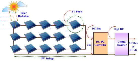
Figure 1.
Photovoltaic Central Inverter Structure (PV-CIS) for transfer of PV energy to an electric grid.
In [4,5,6,7,8], a Photovoltaic String Inverter structure (PV-SIS) is employed to feed photovoltaic energy to the electric grid. In PV-SIS, several PV lines are used, which are made up of several series- connected PV panels as shown in Figure 2. All the PV lines are connected to separate inverters via a DC-DC converter and the inverter outputs are connected in parallel and feed into the electric grid. The drawbacks of the PV-SIS system are: (i) it requires a large number of panels to design a several PV line; (ii) a large number of converters are required to feed the grid; (iii) the cost is high due to the separate MPPT and complex control circuitry is required to synchronize all the inverters.
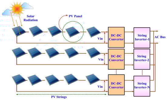
Figure 2.
Photovoltaic String Inverter Structure (PV-SIS) for transfer of PV energy to the electric grid.
In [4,5,6,7,8], Photovoltaic AC Module Structure (PV-ACMS) is discussed to fed photovoltaic energy to the electric grid and it provides a viable solution to overcome the drawbacks of PV-CIS and PV-SIS. In PV-ACMS a single photovoltaic panel is connected to the electric grid via an inverter as shown in Figure 3a. The drawbacks of PV-ACMS are: (i) it requires several module inverters which increase the cost of the system; (ii) separate MPPT is needed for each panel; (iii) the overall efficiency is low. In [4,5,6,7,8], Photovoltaic Multi-String Inverter Structure (PV-MSIS) is discussed to overcome the drawback of PV-CIS, PV-SIS and PV-SIS structures. In PV-MSIS several PV panels are connected to a single inverter connected via several DC-DC converters as shown in Figure 3b. This structure combines the features of PV-SIS and PV-ACMS. The drawback of the PV-MSIS concept is: (i) it required several DC-DC converters to transfer energy to the inverter; (ii) high cost due to the greater number of converters and separate MPPT.
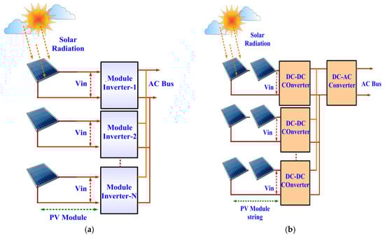
Figure 3.
(a) Photovoltaic AC Module Structure (PV-ACMS); (b) Photovoltaic Multi-String Inverter Structure (PV-MSIS) for transfer of PV energy to the electric grid.
The output obtained from a photovoltaic cell/array is usually low, so before feeding this voltage to the inverter for practical application purposes, it must be stepped up using a conventional DC-DC boost converter [1,2,3,4,5,6,7,8,9,10,11,12,13,14,15]. With the increase in the duty-cycle of switch and leakage resistance of inductors, the performance of the converter degrades. Due to these practical problems, conventional DC-DC converters are unable to provide doable solutions for step-up voltage applications [15]. In theory, when a duty cycle approaches 100%, an infinite voltage conversion ratio is achieved with a conventional boost converter, but in practice, the inductor leakage resistance of the inductor limits the voltage conversion of the converter [16], so the traditional converters cannot be used where the required conversion ratio is four or more [16]. Furthermore, to achieve a high conversion ratio by using large duty cycle compromises the utilization of high frequency for Pulse Width Modulation (PWM) because of semiconductor control devices’ inherent switching delay. Unluckily, a large reactive network follows the limited switching frequency which is employed to protect from the ripple condition of voltage and current [17]. The traditional buck-boost converter is not reliable due to its discontinuous input current, which results in low utilization of the input source [13,15]. By increasing the switching frequency of the converter, the problem of leakage resistance for certain values of ripple can be overcome. The finite switching time in a normal power device limits the switching frequency if the duty ratio is either too high or too small, so in order to abolish the above problems and simultaneously acquire essential high voltage, isolated converters can be engaged. Many isolated and non-isolated converter topologies have proposed over time, which make use of inductors, coupled inductors and transformers [16,17,18,19,20,21,22,23,24,25,26,27]. The high voltage stress occurring due to the transformer leakage inductance leads to switching losses and electromagnetic interference (EMI) problems, resulting in the reduced efficiency of conventional converters. Hard switching converters are inconvenient to use for high voltage applications due to their circuit complexity, higher voltage stress across the switch and the increased cost of the converter. Hence, for isolated topologies the size, weight and losses of power transformers are limiting factors. Recently, various combinations of coupled inductors, voltage multipliers or switched capacitor multipliers [23,24,25,26,27,28,29,30,31,32,33,34,35] along with a switched inductor (SI), switched capacitor (SC), voltage lift switched inductor (VLSI) and modified VLSI principles were used to accomplish the necessity [15,26]. Figure 4a–c shows the recent SI, VLSI and modified VLSI inductive networks. For acquiring a high boost ratio, a cascaded approach is introduced. To design a Cascaded Boost Converter (CBC), a number of inductors are essential, which is the most complex part. In addition, losses and increased current ripple prove to be a barrier to achieve a high conversion ratio and better efficiency [36,37,38]. With an objective of acquiring a high voltage gain just by using a single switch, the Quadratic Boost Converter (QBC) was proposed, though, in a QBC, higher voltage rating switches are required with higher RDS-ON, as voltage stress raised across the switch is equal to the output voltage [39,40,41]. Multilevel converters provide a suitable solution for power conversion because of the low voltage stress across each device [42]. High voltage is achieved by multilevel DC-DC converters using capacitors and diode circuitry at the output end and the output voltage level can be increased without actually disturbing the actual circuit. By varying the number of output levels and duty cycle, the voltage gain of multilevel converters can be varied [43,44]. For conventional multilevel converters, designing magnetic components like inductors is a complex task, which also induces electromagnetic emission noise. Other than these issues the presence of inductors and transformers in the power circuit degrades the integration capability and increases the cost, weight and size of the converters. Switched Capacitor (SC) power circuits provide good integration ability due to their small volume and weight, since magnetic components like transformers and inductors is not needed to design a SC converter [33].
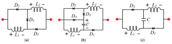
Figure 4.
Inductive networks: (a) Switched Inductor; (b) Voltage Lift switched Inductor cell; (c) modified voltage lift switched inductive cell.
In this article, a new magnetic component-free (transformer-less and inductor-less) DC-DC converter is proposed to overcome the drawbacks of PV-CIS, PV-SIS, PV-ACMS, PV-MSIS and the above discussed converter topology. The proposed converter provides a viable solution for existing photovoltaic application systems where voltage must be stepped up without magnetic components before transferring energy to a multilevel-inverter. The single proposed converter is sufficient to transfer energy to a multilevel inverter as shown in Figure 5.
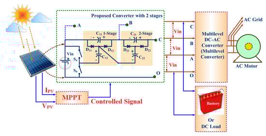
Figure 5.
Proposed multistage self-balanced and magnetic component-free DC-DC converter in a photovoltaic system for the transfer of photovoltaic energy to a DC load, grid or motor.
The proposed photovoltaic system (PV System) consists of PV modules, the proposed DC-DC converter, battery and the multilevel inverter (MLI) which converts the battery/proposed DC-DC converter voltage to AC voltage to power AC loads/feed in the electric grid. Some amount of power is lost during the conversion of photovoltaic energy to electric energy. The PV device maximum output power (product of voltage and current) is described by the Maximum Power Point (MPP) and it is also depends on the environmental conditions (generally on temperature and light conditions). A Maximum Power Point Tracker is compulsory to ensure the maximum power output (Pmax) of a solar PV device. The Maximum Power Point Tracker can be used to adjust its input voltage to utilize the maximum photovoltaic output power and then transform this power to supply the varying voltage requirements. When the PV voltage is increased the current will ultimately decrease, and when the PV current is increased the voltage will ultimately decrease. Depending on parameters like irradiance and temperature the MPP of the I-V curve of a PV module changes dynamically. Therefore, the MPP needs to be located by a tracking algorithm as it is not known beforehand.
To achieve the maximum power transfer from the PV module to the load it is necessary to match the load resistance RL to the best possible output resistance of the PV module RPV (Rmpp = Vmpp/Impp). Characteristic power-voltage and current-voltage graphs or curves are shown in Figure 6a.
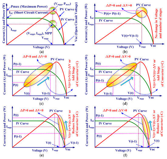
Figure 6.
(a) Power- voltage or current- voltage graphs of a photovoltaic system; (b) MPPT when ∆P = 0 and ∆V = 0; (c) MPPT when ∆P < 0 and ∆V < 0; (d) MPPT when ∆P > 0 and ∆V > 0; (e) MPPT when ∆P > 0 and ∆V < 0; (f) MPPT when ∆P < 0 and ∆V > 0.
The output power of PV module will be zero when the photovoltaic current (IPV) is equal to the short circuit current (ISC) or the photovoltaic voltage (VPV) is equal to the open circuit voltage (VOC). Thus, it is possible to track the maximum power point (MPP) of a photovoltaic cell by regulating the operating voltage of VPV. In [45] Maximum Power Point Tracking is discussed for a reconfigurable switched-capacitor converter and in [46] a perturbation and observation (P&O) algorithm is discussed for DC-DC converters connected to photovoltaic generators. The concept to control power of a multistage magnetic component-free DC-DC converter is explained in Figure 6b–f. Thus, to regulate the operating voltage VPV, the ON time of the capacitor and number of stages (if the structure is reconfigurable) are two controlled parameters in the proposed system, therefore it forces the MPPT charge controller to extract the maximum power PV module to operate at a voltage close to the maximum power point which causes it to draw the maximum available power from the PV module.
The proposed converter is also suitable for the DC link application in DC-AC systems where capacitor voltage balancing is the main challenge. The proposed converter also provides a viable solution for low power applications, since inductors and transformers are not required to design the proposed converter.
2. Recent Transformer-Less and Inductor-Less DC-DC Converters
In this section recent transformer-less and inductor-less DC-DC converter power circuit topologies and their drawbacks are discussed in detail. Various multilevel DC-DC converters and switched capacitor topologies without inductor were recently addressed in the literature.
2.1. Series-Parallel Switched Capacitor (SC) Converter
In [47,48,49], a series-parallel switched capacitor (SPSC or series-parallel SC) converter using only control switching elements and capacitors was proposed. In Figure 7a three-level series-parallel SC converter is depicted. The operation of this topology is simple and divided into only two modes (two switching states only). All the switches are controlled in such a way that all the capacitors are charged in series and discharged in parallel. The conversion ratio of an N-level series-parallel SC converter is 1/N (in step-down mode) and N times (in step-up mode). More than 90% efficiency is reported in the literature.
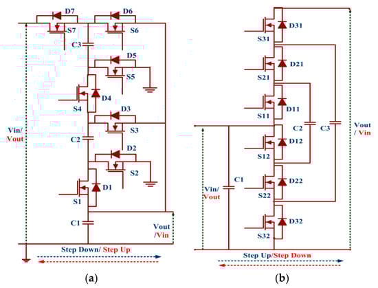
Figure 7.
(a) Three–Level Series-Parallel Switched Capacitor (Series-Parallel SC) Converter; (b) Flying Capacitor Multilevel DC-DC Converter (FCMDC).
However the series-parallel SC converter has following drawbacks:
- Difficult to change the switching state of the converter due to the several switching elements.
- Unequal voltage across switches, thus power switches of various ratings are required.
- Series-parallel SC is bidirectional, but it is not possible to control the power flow. It depends on the voltages at the input and output DC buses.
- If switching is not properly controlled, it may instigate a charge unbalance situation among the converter capacitors.
- Non-modularity, since a large number of switches, gate drivers and diodes are required and the number of devices increases with the number of levels. Due to this a series parallel converter is large in size and has high cost.
2.2. Flying Capacitor Multilevel DC-DC Converter (FCMDC)
In [49,50,51], flying capacitor multilevel DC-DC converter (FCMDC) is proposed. Figure 7b depicts the power circuit of a three–level FCMDC. The conversion ratio of an N-level FCNDC is 1/N (in step-down mode) and N times (in step-up mode). FCMDC is a bidirectional converter with efficiency higher than 95%. The voltage stress of switches is also equal and thus requires same rating of the switching devices. Nevertheless FCMDC has the following drawbacks:
- A large number of transistors and capacitors is required (2N the number of switches and N number of capacitors are required to design an N-level FCMDC), hence this converter is large in size and also has a high cost.
- Difficult to extend the power circuit to increase the number of stages to change the output conversion ratio since the converter does not have a modular structure.
- A complicated switching scheme is required to operate the converter.
- FCMDC is inefficient at high switching frequency when the ON time is comparable to the rise and fall time of the switches since; to transfer energy from the input source to the capacitors a very small time frame is allowed.
- Utilization of components is less. It is not possible to control the power circuit if any of the switches fails.
2.3. Magnetic-Less Multilevel DC-DC Converter (MMDC)
In [52], a magnetic-less multilevel DC-DC converter (MMDC) is proposed by connecting two transistor and one capacitor switching cells (modular block) in a mesh pattern. Figure 8 depicts the power circuitry of the three-level MMDC. The conversion ratio of an N-Level MMDCC is 1/N (in step-down mode) and N times (in step-up mode). The voltage stress of each transistor of the switching cells is the same and equal to Vin and also it is independent of the duty cycle and conversion ratio of the converter. However, the following are the drawbacks of the MMDC:
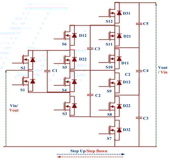
Figure 8.
Three-Level Magnetic-Less Multilevel DC-DC Converter (MMDC).
- A very large number of switching devices and capacitors are required to design an MMDC N (N + 1) switches, N (N + 1) diodes and 0.5N (N + 1) capacitors are required to design the N-Level MMDCC.
- It is difficult to manage direction of power flow of the converter due to the greater number of transistors present in the conducting path.
- The power flow of the converter is also depends on the voltages at the input and output DC buses, thus it is not a good option for the applications where the source voltage may vary.
2.4. Fibonacci DC-DC Converter
In [53], a Fibonacci DC-DC converter is proposed using capacitors and switching device circuitry. The voltage conversion ratio of the converter follows the well-known Fibonacci series. Figure 9 depicts the power circuitry of the three stage-Fibonacci converter. High voltage is achieved but it still requires a large number of switching devices and capacitors. The following are the drawbacks of the Fibonacci DC-DC converter:
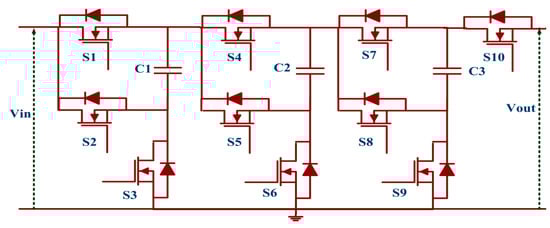
Figure 9.
Three-Level Fibonacci DC-DC converter.
- A large number of control switches are required to design the converter (3N + 1 number of control switches are required to design an N-stage converter)
- The Fibonacci DC-DC converter follows the Fibonacci series and thus it is not possible to achieve voltage conversion ratios like 2, 4… (which are not present in the Fibonacci converter)
- It is not capable of transferring power in both directions.
2.5. Modified Step-Up DC-DC Converter (Switch Mode DC-DC Converter)
In [54], a modified step-up DC-DC converter (switch mode DC-DC converter) is proposed which has continuous input current capability. Figure 10 depicts the switch mode DC-DC converter. Its power circuitry is divided into two parallel parts. A detailed study about the mode of operation and capacitor state is given in Table 1. The operation of the proposed converter is simple and the conversion ratio of the converter is adjusted by varying the duty cycle. In addition, the continuous input current from low voltage input sources reduces the EMI problem.
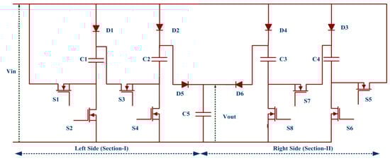
Figure 10.
Modified Step-up DC-DC Converter (Switch Mode DC-DC Converter).

Table 1.
Mode of operation and state of capacitors of Modified Step-up DC-DC Converter.
However this converter has the following drawbacks:
- A large number of switching devices is required.
- It introduces high switching losses and thus the efficiency of the converter is less.
- Moreover, there is no extension of the circuit to increase the voltage conversion ratio.
- This converter is not suitable for high power high voltage applications due to the lower voltage conversion ratio.
2.6. Switched Capacitor DC-DC Converter
In [55], a new switched capacitor DC-DC converter with low ripple input current is proposed. Figure 11 depicts the power circuit of the converter. The low ripple and continuous input current help to reduce EMI of the circuit. However this circuit has no provision to increase the voltage conversion ratio.
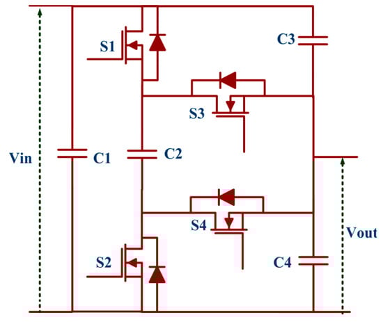
Figure 11.
Switched Capacitor DC-DC Converter.
2.7. Multilevel Modular Capacitor Clamped DC-DC Converter (MMCCC)
In [56], a multilevel modular capacitor clamped DC-DC converter (MMCCC) is proposed. Figure 12 depicts the power circuit of the MMCCC for five levels. The following are the drawbacks of the MMCCC:
Figure 12.
Multilevel Modular Capacitor Clamped DC-DC Converter (MMCCC).
- Using this topology a high voltage conversion ratio is achieved, but it requires a large number of switching devices and capacitors.
- The voltage stress across switches of the converter is high. For an N level MMCCC the voltage stress of N-2 switching devices is equal to 2Vin and the remaining switches have Vin voltage stress.
3. Proposed Self-Balanced and Magnetic Component-Free Multistage DC-DC Converter
3.1. Mode of Operation
The power circuit of the proposed self balanced and magnetic component-free (transformer-less and inductor-less) multistage DC-DC converter for K stages is depicted in Figure 13. The conspicuous features of the proposed topology are: (i) it is magnetic components free; (ii) continuous input current; (iii) low voltage rating semiconductor devices and capacitors; (iv) modularity; (v) easy to add a higher number of levels to increase the voltage; (vi) only two control switches are used with alternating operation; and (vii) simple control. The proposed DC-DC converter topology is free from magnetic components like inductors and it is designed for unidirectional power transfer applications. The proposed topology provides an output voltage higher than the input voltage without any magnetic components. The operation at high frequency permits a reduction in the size of capacitors thus enabling a reduced size of the circuit without external components. In this topology the number of control switches does not depend on the number of levels. The required number of diodes and capacitors depends on the number of output levels. Two diodes and two capacitors are required to increase the level of the proposed converter by one. Thus, to design a 4-stage proposed step-up DC-DC converter topology, two control switches, eight uncontrolled (power diodes) and eight capacitors are required.
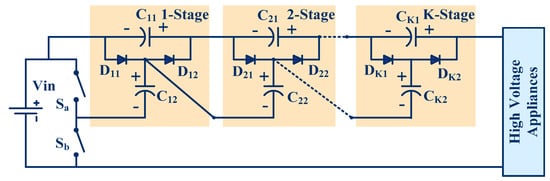
Figure 13.
Self-balanced and magnetic component-free multistage converter for K stages.
To explain the operation modes of the proposed magnetic component-free K-stages converter circuit the following is considered. The mode of operation of the converter is divided into two modes: Mode 1 when switch Sb and Sa act as a short circuit (turned ON) and open circuit (turned OFF) respectively, and Mode 2 when switch Sa and Sb act as a short circuit (turned ON) and open circuit (turned OFF), respectively. Hence, switch Sa and switch Sb are complementary in operation. The proposed topology has simple control and is operated at a fixed duty cycle of 0.5 to provide voltage to photovoltaic devices. A complex gate driver is also not required to drive the switch; instead an oscillator is sufficient to provide a gated signal.
In Mode 1 (Figure 14), switch Sb is turned ON and switch Sa is turned OFF, capacitor C12 is charged by input voltage through diode D11 and switch Sb when the voltage across capacitor C12 is smaller than the input voltage. When the voltage across capacitors C12 + C22 is smaller than the voltage VC11 + Vin, then the energy stored in the capacitor C11 is transferred to capacitor C22 through D21 and switch Sb. Similarly capacitor C(k-1)1 transfers its energy to CK2 when the voltage across capacitors C12 + C22 +… + CK2 is smaller than voltage Vin + VC11 + CC21 +… + VC(K-1)1 through diode DK1. In this mode the output voltage is equal to the input voltage (Vin) + VC11+VC21 +…+ VCK1.
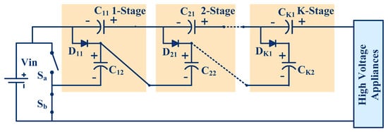
Figure 14.
Switch Sb of proposed magnetic component free multistage DC-DC converter is ON.
In Mode 2 (Figure 15), control switch Sa is turned ON and switch Sb is turned OFF, when the voltage across capacitor C11 is smaller than capacitor C12, then capacitor C11 is charged by capacitor C12 through diode D12 and switch Sa. When the voltage across capacitor C11 + C21 is smaller than the voltage across capacitor C12 + C22, then capacitor C22 transfers its energy to capacitor C21 through diode D22 and switch Sa. Similarly capacitor CK2 transfers its energy to capacitor CK1 through DK2 when the voltage across capacitor C11 + C21+…+ Ck1 is smaller than the voltage C12 + C22 + CK2. In this mode the output voltage is equal to the input voltage (Vin) + VC12 + VC22 + …+ VCK2.
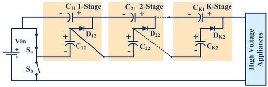
Figure 15.
Switch Sa of proposed magnetic component free multistage DC-DC converter is ON.
3.2. Voltage Gain Analysis of a Multistage Converter without Diode and Switches Loss
When the voltage drop across diodes and switches are not considered, all capacitors are subjected to the same voltage Vin. The voltage conversion ratio or voltage gain is equal to the (K + 1) i.e., number of stages +1 and also depends on number of capacitors. Figure 16a,b depict the graphs of the required number of devices/components versus the number of stages in 2-dimensional and in 3-dimensional view, respectively. From Figure 16a,b it is observed that the number of devices/components linearly increases as the number of stages is increased. Thus, with each stage increase two more diodes and capacitors are needed. It is also observed that the number of diodes is equal to the number of capacitors.
where, KC and KD number of capacitor and diode used to design the proposed circuit. The graph of voltage gain versus number of stages is shown in Figure 17a. It is observed that the proposed converter with K stages provides a K + 1 voltage conversion ratio. The graph of the number of stage devices/components versus voltage gain is shown in Figure 17b. It is observed that the number of devices/components linearly increases as the voltage gain requirement is increased. Thus, two diodes and two capacitors need to be connected to increase voltage gain by a factor of 1. It is also observed that 2 K diodes and 2 K capacitors are required to attain a voltage gain K + 1.
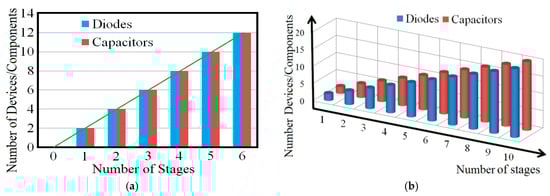
Figure 16.
Number of devices/components versus the number of stages (a) 2-dimensional view; (b) 3-dimensional view.
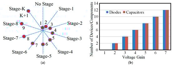
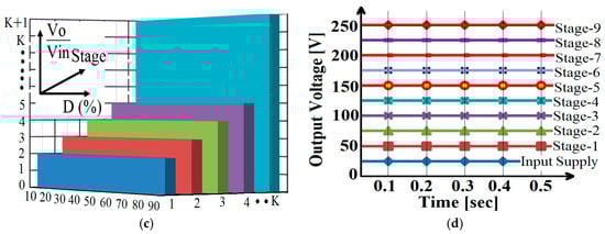
Figure 17.
Relations of converter parameters: (a) graph of voltage gain versus number of stages; (b) graph of the number of devices/component versus voltage gain; (c) graph of the voltage gain (Vo/Vin), number of stages (K) and duty cycle (D); (d) output voltage for stage 1 to 9 for 25 V input voltage.
The graph of voltage gain (Vo/Vin), number of stages (K) and duty cycle (D) is shown in Figure 17c. It is observed that two capacitors and two diodes are required to design one stage of the proposed converter. The graph of output voltage for stages 1 to 9 by considering an input voltage of 25 V is shown in Figure 17d. It is observed that the output voltage is increased as the number of stages increases, and each stage contributes a voltage equal to the input voltage (25 V) to an output voltage of the proposed converter.
3.3. Voltage Gain Analysis of the Multistage Converter with Diode and Switches Loss
The voltage drop across power diodes and switches is ignored in medium and high power applications, but in low power applications it is considered. The analysis of the circuit is done with consideration of the voltage drop across diodes and switches. For simplicity, the voltage drop across diodes and switches is assumed to be equal to Vd.
It is investigated that the voltage across each capacitor is equal to Vin − 4Vd except for the voltage across capacitor C12. The voltage across capacitor C12 is equal to Vin − 2Vd. Thus, the proposed topology is self-balanced and magnetic component-free. The output voltage of the converter is limited by the devices’ forward voltage and number of devices.
The graph of the proposed converter output voltage versus number of stages with a practical diode (Vd = 1) and ideal diode is shown in Figure 18a. The graph of the proposed converter output voltage versus number of diodes or capacitors with a practical diode (Vd = 1) and an ideal diode is shown in Figure 18b. From Figure 18a,b it is observed that the difference between the ideal and practical output voltage increases as the number of stages, diodes and capacitor requirement is increased. The difference between the ideal and practical output voltage depends on the number of stages of the proposed converter and it is equal to 4KVd as given in Equation (15).
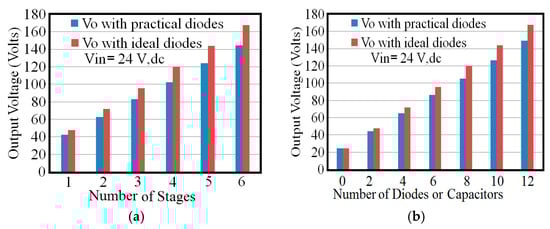
Figure 18.
Comparison graph considering Vin = 24 V. (a) Graph of converter output voltage versus number of stages (practical and ideal diode); (b) graph of converter output voltage versus number of diodes or capacitors (practical and ideal diode).
4. Design Calculation of the Capacitors of the Proposed Converter
To explain the designed calculation of the proposed converter a 1-stage proposed converter is considered. The power circuit of the 1-stage proposed converter is shown in Figure 19a. The ON state and OFF state equivalent circuit of the 1-stage proposed converter is depicted in Figure 19b,c respectively, where RD is the forward resistance of the diode, RS is the forward resistance of the switch, ISb is the current through the switch Sb and ISa is the current through switch Sa.
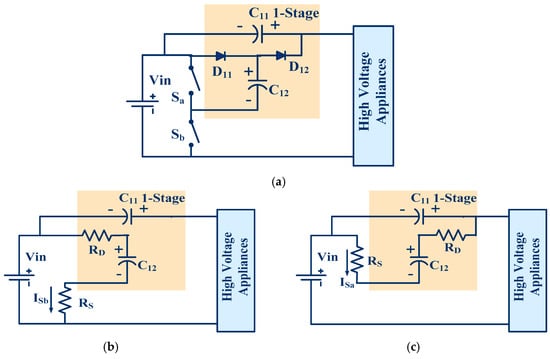
Figure 19.
(a) Power circuit of the 1-stage proposed converter; (b) equivalent circuit of 1-stage proposed converter when Sb is ON; (c) equivalent circuit of 1-stage proposed converter when Sa is ON.
Initially the voltage across capacitor C12 and C11 is zero. Capacitor C12 is charged through a resistance RD and RS from a supply voltage Vin when switch Sb is closed. The voltage across C12 does not increase to Vin instantaneously, but builds up exponentially and not linearly.
Similarly:
Capacitor C11 is charged through a resistance RD and RS from a capacitor C12 voltage when switch Sa is closed. Thus, when switch Sa is closed capacitors C11 and C12 is charging and discharging, respectively.
Similarly:
In steady state and at high switching frequency, the voltage across capacitor C11 and C12 at any instant during charging is cycled as given in Equations (25) and (26) where, and is the initial voltage of capacitor C11 and C12. If the initial storage voltage of C11 and C12 is positive:
If the initial storage voltage of C11 and C12 is negative:
The time required for the capacitor C12 to attain any value of VC12 during the charging cycle is given in Equations (27) and (28).
When the initial voltage across the capacitor is positive:
When the initial voltage across the capacitor is negative:
The time required for the capacitor C11 to attain any value of VC11 during the charging cycle is given in Equations (29) and (30).
When the initial voltage across the capacitor is positive:
When the initial voltage across the capacitor is negative:
Voltage and current of all the capacitors are the same during the complete switching cycle. Thus the equal rating of all capacitors is suitable to design the proposed converter whose voltage rating is greater than the input voltage.
5. Comparison of Proposed Converter with Recent DC-DC Inductor-less Converters
In this section the proposed circuit is compared with recent transformer-less and inductor-less DC-DC converters (discussed in Section 2 of this article) in terms of number of controlled switches, diodes, capacitors, and voltage gain. The requirement of the number of switches to design DC-DC converters is tabulated in Table 2.
Table 2.
Number of switches required to design different DC-DC converters.
It is observed that proposed converter requires less switches compared to other recent transformer-less and inductor-less converters. It is also observed that the requirement of switches is independent of the number of levels of the converter (only two switches are required to design the proposed converter). It is also observed that the requirement of the number of switches to design and MMCCC is the same. The requirement of the number of diodes and number of capacitors to design DC-DC converters is tabulated in Table 3 and Table 4, respectively. It is observed that the proposed converter requires less diodes compared to recently proposed transformer-less and inductor-less DC-DC converters. The maximum number of diodes is required to design the Fibonacci converter. To design SPSC and MMCCC the number of diodes requirement is the same. It is observed that the proposed converter requires less capacitors compared to MMDCC and the switch mode converter. The proposed converter also requires fewer components in total compared to the other converters. In Table 5 voltage conversion ratio of recent inductor-less DC-DC converter is tabulated.
Table 3.
Number of diodes required to design the DC-DC converters.
Table 4.
Number of capacitors required to design the DC-DC converters.
Table 5.
Voltage conversion ratio of the DC-DC converters.
In Figure 20a–d the proposed converter is compared with DC-DC converters (discussed in Section 2) in terms of number of switches, diodes, capacitors and voltage gain. Graphically it is also observed that the proposed converter provides a viable solution in terms of number of components. In Table 6 the proposed converter is compared in terms of cost. It is calculated that the proposed converter required less cost compared to other DC-DC converters. Only two switches are required to design an N-stage proposed converter hence it requires a simple control circuit.
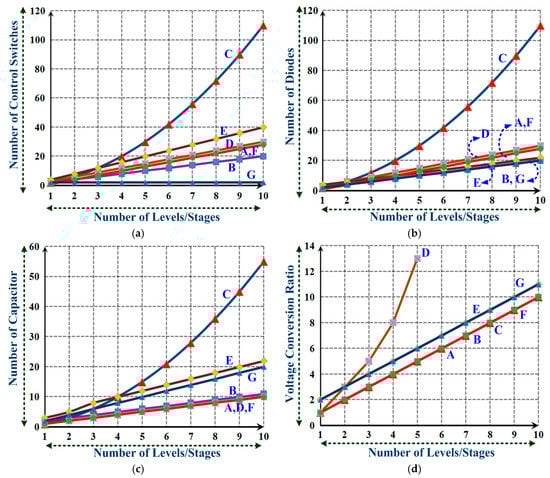
Figure 20.
Comparison of the proposed converter with recent transformer-less and inductor-less converters (Discussed in Section 2) (a) Graph of the number of switches versus number of levels/stages; (b) graph of the number of diodes versus number of levels/stages; (c) graph of the number of capacitors versus number of levels/stages; (d) graph of the voltage conversion ratio versus number of levels/stages. (A: SPSC, B: FCMDC, C: MMDC, D: Fibonacci, E: switch mode, F: MMCCC, G: proposed converter).
Table 6.
Cost of the proposed and recent DC-DC converters (discussed in Section 2).
6. Experimental and Simulation Results of the Proposed Self-Balanced and Magnetic Component-Free Multistage DC-DC Converter
The proposed self-balanced and magnetic component-free multistage DC-DC converter simulation and experimental results are discussed in this section. The proposed multistage converter has been designed for four stages with rated power 60 W, switching frequency 100 kHz, output voltage is 100 V and the supply voltage is 24 V. Switches Sa (here S1) and Sb (here S2) are operated complementarily with a 50% duty cycle. High switching frequency is used to reduce the rating of the capacitor.
The output voltage and current waveform with ideal components (voltage drop across the switch and the diode is zero) is shown in Figure 21a. It is observed that the settling time for the output voltage of the proposed converter with ideal components (forward resistance of the diode is 0) is less than 2 ms. The effect of voltage drop across the diode is analyzed in the previous section. The output voltage and current waveform (assuming 1 V voltage drop across the switch and diode) are shown in Figure 21b.
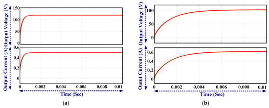
Figure 21.
Simulation results (a) Output voltage and current waveform with ideal components and Vin = 24 V; (b) Output voltage and current waveform with practical components and Vin = 24 V.
It is observed that the settling time for the output voltage of the proposed converter with practical components is approximately 4 ms due to the forward resistance of the diode and switch. Thus, the practical waveform differs from the ideal waveform because of the time constant (RD + RS) C as explained in Section 4. The output power waveform and switch voltage are shown in Figure 22a,b, respectively. The output voltage and input voltage waveform with ideal components (voltage drop across the switch and the diode is zero) are shown in Figure 22c. The output voltage and input voltage waveform (assuming a 1 V voltage drop across the switch and diode) are shown in Figure 22d.
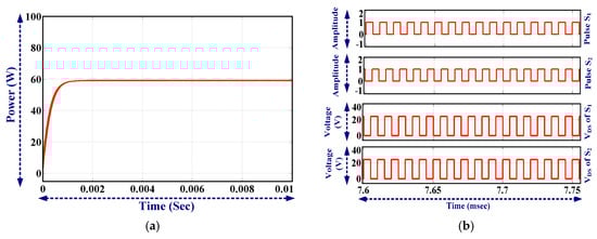
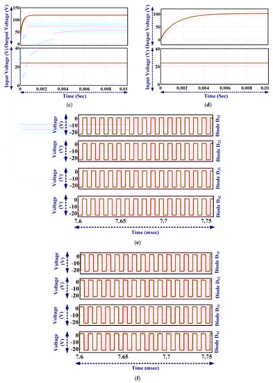
Figure 22.
Simulation results (a) Output power of proposed converter; (b) Gate pulses to control switches of the converter and drain to source of the converter; (c) Output voltage and input voltage waveform with ideal components; (d) Output voltage and input voltage waveform with practical components; (e) Voltage across diode D11, D21, D31 and D41; (f) Voltage across diode D12, D22, D32 and D42.
It is observed that 120 V output voltage is achieved from a 24 V input supply. Thus, ideally the voltage gain of the proposed converter is 5, which is equal to the number of stages +1. When the voltage drop across the diode is considered, an output voltage of 100 V is achieved from a 24 V supply. The voltage across the switch is equal to the input supply voltage (24 V). The voltage across all capacitors is same, which is equal to the input supply voltage (24 V) if the voltage drop across the diode is not considered. The voltage across all diodes is same (24 V) when the diode is reverse- biased. The voltage across diodes is shown in Figure 22e–f. The voltage across the capacitors is shown in Figure 23. The proposed 4-stage self-balanced and magnetic DC-DC converter is investigated experimentally and the result shows a good match with the simulation results. The hardware components are listed in Table 7.
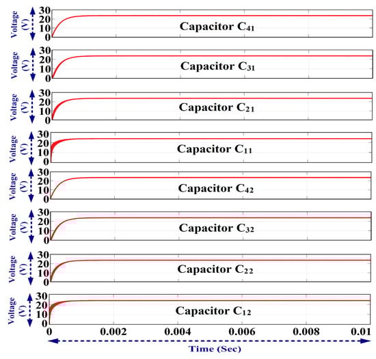
Figure 23.
Voltage across capacitor C41, C31, C21 C11, C42, C32, C22 and C12 (Top to bottom in figure).
Table 7.
Hardware component details of the proposed converter.
PIC18F45K20 is used to generate pulses and TLP250 is used as driver IC. The hardware prototype of the proposed converter is shown in Figure 24.
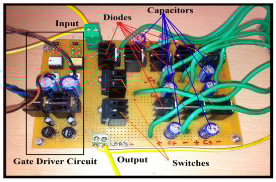
Figure 24.
Hardware prototype of the proposed DC-DC converter.
Pulses are generated from a PIC controller and the gate driver output is shown in Figure 25a,b, respectively. Output voltage and input voltage waveform are shown in Figure 25c. It is observed that 100 V output is achieved from a 24 V input supply.
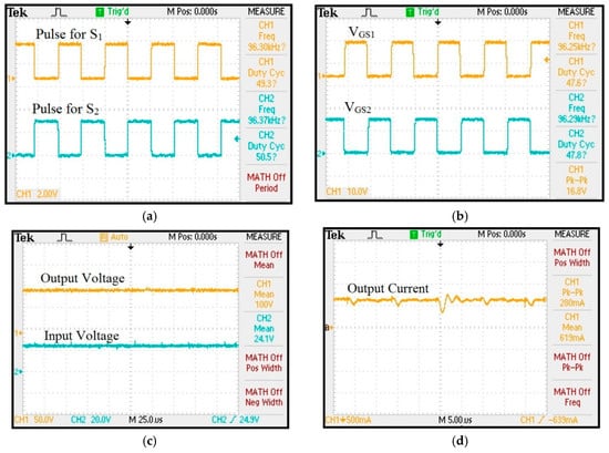
Figure 25.
(a) PIC controller output; (b) TLP 250 gate driver output; (c) Output voltage and input voltage waveform; (d) Output current waveforms.
The output current waveform is shown in Figure 25d and it is observed that the output current is 0.619 A. The voltage across each capacitor is shown in Figure 26a–h. It is observed that the voltage across each capacitor is nearly the same and slightly less than the input voltage 24 V (an effect of the diode). Voltage stress across each diode is shown in Figure 27a–h. It is observed that the voltage stress across the diode is approximately the same and the peak voltage across the diode is slightly less than the input voltage (24 V) (an effect of the voltage drop). The voltages of all capacitors and all diodes differ slightly due to the forward resistance of the diode and switch. The lower stages (source side) capacitors are charged through the path which contain less diodes whereas as the number of stages increases the path followed for the charging of higher stage (moving towards load) capacitors contain more diodes. Thus, practically a slight difference is observed in the voltage of the capacitors.
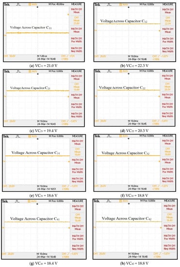
Figure 26.
Capacitors voltage (a) C11 (b) C12 (c) C21 (d) C22 (e) C31 (f) C32 (g) C41 (h) C42.
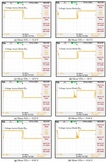
Figure 27.
Voltage across diodes (a) D11 (b) D12 (c) D21 (d) D22 (e) D31 (f) D32 (g) D41 (h) D42.
7. Conclusions
The self-biased and magnetic-free multistage step-up converter is articulated and designed for unidirectional renewable photovoltaic applications. The proposed converter is well suited for renewable photovoltaic applications where the voltage needs to be stepped up without using magnetic components. The proposed converter also provides a viable solution to improve the photovoltaic systems in term of modularity, cost and control. The proposed converter is suitable for the DC link applications in DC-AC systems where capacitor voltage balancing is the main challenge. The proposed converter also provides a viable solution for low power applications, since the inductor and transformer are not required to design the proposed converter. Also Maximum Power Point Tracking (MPPT) can be easily implemented to improve the efficiency of the converter. The voltage across the switch is less; hence low voltage switches are used for designing high voltage converters. The conspicuous features of the proposed topology are:
- (i)
- Magnetic component-free (transformer-less and inductor-less)
- (ii)
- Continuous input current
- (iii)
- Low voltage rating semiconductor devices and capacitors
- (iv)
- Modularity
- (v)
- Easy to add a higher number of levels to increase the voltage
- (vi)
- Only two control switches with alternating operation and simple control are needed.
The proposed converter has been designed with a rated power of 60 W, the input voltage is 24 V, the output voltage is 100 V and the switching frequency is 100 kHz. High switching frequency has been used to decrease the component size. The performance of the proposed converter is verified through simulation and experimental results.
Author Contributions
M.S.B. and S.P. developed the proposed research concept with the complete theoretical background study. Further hardware prototype implementation tasks are carried out the same authors. F.B. has contributed his expertise to validate the proposal both theoretical background and hardware results obtained as co-author. All authors involved in framing its current format of the full research paper work.
Conflicts of Interest
The authors declare no conflict of interest.
References
- Ajami, A.; Ardi, H.; Farakhor, A. A novel high step-up DC/DC converter based on integrating coupled inductor and switched-capacitor techniques for renewable energy applications. IEEE Trans. Power Electron. 2015, 30, 4255–4263. [Google Scholar] [CrossRef]
- Sanjeevikumar, P.; Grandi, G.; Wheeler, P.; Blaabjerg, F.; Loncarski, J. A Simple MPPT Algorithm for Novel PV Power Generation system by High Output Voltage DC-DC Boost Converter. In Proceedings of the 24th IEEE International Symposium on Industrial Electronics, Rio de Janeiro, Brazil, 3–5 June 2015; pp. 214–220. [Google Scholar]
- Siwakoti, Y.; Blaabjerg, F. A Novel Flying Capacitor Transformerless Inverter for Single-Phase Grid Connected Solar Photovoltaic System. In Proceedings of the 7th International Symposium on Power Electronics for Distributed Generation Systems (PEDG), Vancouver, Canada, 27–30 June 2016. [Google Scholar]
- Kleinkauf, W.; Cramer, G.; Ibrahim, M. PV Systems Technology-State of the Art Developments and Trends in Remote Electrification; SMA Technologies AG: Fountain Valley, CA, USA, 2005. [Google Scholar]
- Calais, M.; Agelidis, V. Multilevel converters for single-phase grid connected photovoltaic systems, an overview. In Proceedings of the IEEE International Symposium on Industrial Electronics (IEEE-ISIE’08), Pretoria, South Africa, 7–10 July 1998; pp. 224–229. [Google Scholar]
- Jenkins, N. Photovoltaic systems for small-scale remote power supplies. J. Power Eng. 1995, 9, 89–96. [Google Scholar] [CrossRef]
- Kjaer, S.B.; Pedersen, J.K.; Blaabjerg, F. A review of single phase grid connected inverters for photovoltaic modules. IEEE Trans. Ind. Appl. 2005, 41, 1292–1306. [Google Scholar] [CrossRef]
- Blaabjerg, F.; Iov, F.; Kerekes, T.; Teodorescu, R. Trends in Power Electronics and Control of Renewable Energy Systems. In Proceedings of the 14th IEEE International Power Electronics and Motion Control Conference, EPE-PEMC, Metropol Lake Resort Ohrid, Macedonia, 6–8 September 2010. [Google Scholar]
- Sabzali, A.J.; Ismail, E.H.; Behbehani, H.M. High voltage step-up integrated double Boost-Sepic DC–DC converter for fuel-cell and photovoltaic applications. Elsevier J. Renew. Energy 2015, 82, 44–53. [Google Scholar] [CrossRef]
- Sanjeevikumar, P.; Grandi, G.; Blaabjerg, F.; Wheeler, P.; Siano, P.; Hammami, M. A Comprehensive Analysis and Hardware Implementation of Control Strategies for High Output Voltage DC-DC Boost Power Converter. Int. J. Comput. Intell. Syst. (IJCIS) 2017, 10, 140–152. [Google Scholar]
- Wuhua, L.; Xiangning, H. Review f nonisolated high-step-up dc/dc converters in photovoltaic grid-connected applications. IEEE Trans. Ind. Electron. 2011, 58, 1239–1250. [Google Scholar]
- Kuo-ching, T.; Chi-Chih, H.; Chun, A.C. A high step-up converter with a voltage multiplier module for a photovoltaic system. IEEE Trans. Power Electron. 2013, 28, 3047–3057. [Google Scholar]
- Mahajan, S.B.; Sanjeevikumar, P.; Wheeler, P.; Blaabjerg, F.; Rivera, M.; Kulkarni, R. XY Converter Family: A New Breed of Buck Boost Converter for High Step-up Renewable Energy Applications. In Proceedings of the IEEE International Conference on Automatica, XXII Congress of the Chilean Association of Automatic Control, Talca, Chile, 19–21 October 2016. [Google Scholar]
- Sanjeevikumar, P.; Kabalci, E.; Iqbal, A.; Abu-Rub, H.; Ojo, O. Control Strategy and Hardware Implementation for DC-DC Boost Power Conversion Based on Proportional-Integral Compensator for High Voltage Application. Eng. Sci. Tech. Int. J. (JESTECH) 2014, 18, 163–170. [Google Scholar]
- Mahajan, S.B.; Sanjeevikumar, P.; Blaabjerg, F.; Kulkarni, R.; Seshagiri, S.; Hajizadeh, A. Novel LY Converter Topologies for High Gain Transfer Ratio-A New Breed of XY Family. In Proceedings of the 4th IET International Conference on Clean Energy and Technology (IET_CEAT16), Kuala Lumpur, Malaysia, 14–15 November 2016. [Google Scholar]
- Rosas Caro, J.C.; Fernando, M.; Mayo-Maldonado, J.; Gonzalez, J.M.; Halida, L.; Jejus, E. Transformer-less high gain boost converter with input current ripple cancelation at a selectable duty cycle. IEEE Trans. Ind. Electron. 2013, 60, 4492–4499. [Google Scholar] [CrossRef]
- Valdez-Reséndiza, J.E.; Claudio-Sáncheza, A.; Rosas-Carob, J.C.; Guerrero-Ramíreza, G.V.; Mayo-Maldonadoc, J.C.; Tapia-Hernándeza, A. Resonant Switched capacitor voltage multiplier with Interleaving capability. Electr. Power Syst. Res. 2016, 133, 365–372. [Google Scholar] [CrossRef]
- Yang, L.S.; Liang, T.J.; Lee, H.C.; Chen, J.F. Novel high step-up DCDC converter with coupled-inductor and voltage-doubler circuits. IEEE Trans. Ind. Electron. 2011, 58, 4196–4206. [Google Scholar] [CrossRef]
- Hsieh, Y.P.; Chen, J.F.; Liang, T.J.; Yang, L.S. Novel high step up DC-DC converter with coupled inductor and switch-capacitor techniques. IEEE Trans. Ind. Electron. 2012, 59, 998–1007. [Google Scholar] [CrossRef]
- Changchien, S.K.; Liang, T.J.; Chen, J.; Yang, L.S. Step-up DC-DC converter by coupled inductor and voltage-lift technique. IET Power Electron. 2010, 3, 369–378. [Google Scholar] [CrossRef]
- Keum, M.; Choi, Y.; Han, S.; Kang, J. High efficiency voltage clamped coupled inductor boost converter. In Proceedings of the IEEE Industrial Electronics Society 39th Annual Conference, Vienna, Austria, 10–13 November 2013. [Google Scholar]
- Siwakoti, Y.P.; Loh, P.C.; Blaabjerg, F.; Andreasen, S.J.; Town, G.E. Y-Source Impedance Network Based Boost DC/DC Converter for Distributed Generation. IEEE Trans. Ind. Electron. 2015, 62, 1059–1069. [Google Scholar] [CrossRef]
- Siwakoti, Y.P.; Loh, P.C.; Blaabjerg, F.; Loh, P.C. High Step-Up Trans-Inverse (Tx-1) DC-DC Converter for Distributed Generation System. IEEE Trans. Ind. Electron. 2016, 63, 4278–4291. [Google Scholar] [CrossRef]
- Forouzesh, M.; Siwakoti, Y.; Gorji, S.; Blaabjerg, F.; Lehman, B. A Survey on Voltage Boosting Techniques for Step-Up DC-DC Converters. In Proceedings of the IEEE Energy Conversion Congress and Exposition (ECCE), Milwaukee, WI, USA, 18–22 September 2016. [Google Scholar]
- Muhammad, M.; Armstrong, M.; Elgendy, M. Non-isolated interleaved DC–DC converter for high voltage gain applications. IEEE J. Emerg. Sel. Top. Power Electron. 2016, 4, 352–362. [Google Scholar] [CrossRef]
- Chen, S.; Lao, M.; Hsieh, Y.; Laing, T.; Chen, K. A novel switched-coupled inductor DC-DC step-up converter and its derivatives. IEEE Trans. Ind. Appl. 2015, 51, 309–314. [Google Scholar] [CrossRef]
- Hwu, K.; Jiang, W.; Yang, L. High-step-up single-switch DC-DC converter with low voltage spike. IET Power Electron. 2015, 8, 2504–2510. [Google Scholar] [CrossRef]
- Mahajan, S.B.; Sanjeevikumar, P.; Blaabjerg, F.; Norum, L.; Ertas, A. 4Nx Non-Isolated and Non-Inverting Hybrid Interleaved Boost Converter Based On VLSI Cell and Cockroft Walton Voltage Multiplier for Renewable Energy Applications. In Proceedings of the IEEE International Conference on Power Electronics, Drives and Energy Systems, Trivandrum, India, 14–17 December 2016. [Google Scholar]
- Chen, Z.; Zhou, Q.; Xu, J. Coupled-inductor boost integrated flyback converter with high-voltage gain and ripple-free input current. IET Power Electron. 2015, 8, 213–220. [Google Scholar] [CrossRef]
- Chen, Y.; Tsai, M.; Laing, R. DC–DC converter with high voltage gain and reduced switch stress. IET Power Electron. 2014, 7, 2564–2571. [Google Scholar] [CrossRef]
- Rosas Caro, J.C.; Salas-cabrera, R.; Mayo-Maldonado, J. A Novel Two Switches Based DC-DC Multilevel Voltage Multiplier. Glob. J. Res. Eng. 2010, 10, 101–105. [Google Scholar]
- Tang, Y.; Fu, D.; Kan, J.; Wang, T. Dual switches DC–DC converter with three winding-coupled inductor and charge pump. IEEE Trans. Power Electron. 2016, 31, 461–469. [Google Scholar] [CrossRef]
- Mayo-Maldonado, J.; Rosas Caro, J.C.; Rapsisarada, P. Modeling Approaches for DC–DC Converters with Switched Capacitors. IEEE Trans. Ind. Electron. 2015, 62, 953–959. [Google Scholar] [CrossRef]
- Prudente, M.; Pfitscher, L.; Emmendoerfer, G.; Romaneli, E.; Gules, R. Voltage Multiplier Cells Applied to Non-Isolated DC–DC Converters. IEEE Trans. Power Electron. 2008, 23, 871–887. [Google Scholar] [CrossRef]
- Shen, M.; Peng, F.; Tolbert, L. Multilevel DC-DC power conversion system with mutliple DC source. IEEE Trans. Power Electron. 2008, 23, 420–426. [Google Scholar] [CrossRef]
- Bratcu, A.; Munteanu, I.; Bacha, S.; Picault, D.; Raison, B. Cascaded dc–dc converter photovoltaic systems: Power optimization issues. IEEE Trans. Ind. Electron. 2011, 58, 403–411. [Google Scholar] [CrossRef]
- Chen, S.; Liang, T.; Yang, L.; Chen, J. A Cascaded High Step-Up DC-DC Converter with Single Switch for Microsource Applications. IEEE Trans. Power Electron. 2011, 26, 1146–1153. [Google Scholar] [CrossRef]
- Walker, G.; Sernia, C. Cascaded DC-DC converter connection of photovoltaic modules. IEEE Trans. Power Electron. 2004, 19, 1130–1139. [Google Scholar] [CrossRef]
- Ye, Y.; Cheng, K. Quadratic Boost Converter with Low Buffer capacitor stress. IET Power Electron. 2014, 7, 1162–1170. [Google Scholar] [CrossRef]
- Al-saffar, M.; Ismail, E.; Sabzali, A. High effieceny quadtraic Boost Converter. In Proceedings of the 27th Annual IEEE Applied Power Electronics Conference and Exposition (APEC), Orlando, FL, USA, 5–9 February 2012; pp. 1245–1252. [Google Scholar]
- Loera-Palomo, R.; Morales-Saldaña, J. Family of quadratic step-up dc–dc converters based on non-cascading structures. IET Power Electron. 2015, 8, 793–801. [Google Scholar] [CrossRef]
- Rosas-Caro, J.C.; Ramirez, J.; Peng, F.Z.; Valderrabano, A. A DC-DC multilevel boost converter. IET Power Electron. 2010, 3, 129–137. [Google Scholar] [CrossRef]
- Mahajan, S.B.; Kulkarni, R.; Sanjeevikumar, P.; Siano, P.; Blaabjerg, F. Hybrid Non-Isolated and Non Inverting Nx Interleaved DC-DC Multilevel Boost Converter For Renewable Energy Applications. In Proceedings of the 16th IEEE International Conference on Environment and Electrical Engineering, Florence, Italy, 7–10 June 2016. [Google Scholar]
- Mahajan, S.B.; Kulkarni, R.; Sanjeevikumar, P.; Blaabjerg, F.; Fedák, V.; Cernat, M. Non Isolated and Non-Inverting Cockcroft Walton Multiplier Based Hybrid 2Nx Interleaved Boost Converter for Renewable Energy Applications. In Proceedings of the IEEE Conference on 17th the Power Electronics and Motion Control, Varna, Bulgaria, 25–30 September 2016. [Google Scholar]
- Chang, Y.H.; Chen, C.L.; Lin, T.C. Reconfigurable Switched-Capacitor Converter for Maximum Power Point Tracking of PV System. In Proceedings of the International Multi Conference of Engineers and Computer Scientists (IMECS), Hong Kong, China, 12–14 March 2014. [Google Scholar]
- Kolsi, S.; Samet, H.; Amar, M.B. Design Analysis of DC-DC Converters Connected to a Photovoltaic Generator and Controlled by MPPT for Optimal Energy Transfer throughout a Clear Day. J. Power Energy Eng. 2014, 2, 27–34. [Google Scholar] [CrossRef]
- Harris, W.; Ngo, K. Power Switched-Capacitor DC-DC Converter, Analysis and Design. IEEE Trans. Aerosp. Electron. Syst. 1997, 33, 386–395. [Google Scholar] [CrossRef]
- Viraj, A.; Amaratunga, G. Analysis of Switched Capacitor DC-DC Step Down Converter. In Proceedings of the IEEE International Symposium on Circuits and Systems (IEEE/ISCAS), Vancouver, BC, Canada, 23–26 May 2004; Volume 5, pp. 836–839. [Google Scholar]
- Pan, Z.; Zhang, F.; Peng, F.Z. Power Losses and Efficiency Analysis of Multilevel DC-DC Converters. In Proceedings of the IEEE Applied Power Electronics Conference and Exposition (IEEE/APEC), Austin, TX, USA, 6–10 March 2005; pp. 1393–1398. [Google Scholar]
- Zhang, F.; Du, L.; Peng, F.Z.; Qian, Z. A New Design Method for High Efficiency DC-DC Converters with Flying Capacitor Technology. In Proceedings of the IEEE Applied Power Electronics Conference and Exposition (IEEE/APEC), Dallas, TX, USA, 19–23 March 2006; pp. 92–96. [Google Scholar]
- Zhang, F.; Peng, F.Z.; Qian, Z. Study of the Multilevel Converter in DC-DC Applications. In Proceedings of the IEEE Power Electronics Specialists Conference (IEEE/PESC), Aachen, Germany, 20–25 June 2004; pp. 1702–1706. [Google Scholar]
- Peng, F.Z.; Zhang, F.; Qian, Z. A Magnetic-Less DC-DC Converter for Dual-Voltage Automotive Systems. IEEE Trans. Ind. Appl. 2003, 39, 511–518. [Google Scholar] [CrossRef]
- Makowski, M.S.; Maksimovic, D. Performance Limits of Switched-Capacitor DC-DC Converters. In Proceedings of the IEEE Power Electronics Specialists Conference (IEEE/PESC), Atlanta, GA, USA, 18–22 June 1995; Volume 2, pp. 1215–1221. [Google Scholar]
- Mak, O.; Wong, Y.; Ioinovici, A. Step-up DC Power Supply Based on a Switched-Capacitor Circuit. IEEE Trans. Ind. Electron. 1995, 42, 90–97. [Google Scholar]
- Umeno, T.; Takahashi, K.; Oota, I.; Ueno, F.; Inoue, T. New Switched-Capacitor DC-DC Converter with Low Input Current and Its Hybridization. In Proceedings of the 33rd Midwest Symposium on Circuits and Systems, Calgary, AB, Canada, 10–12 August 1990; Volume 2, pp. 1091–1094. [Google Scholar]
- Khan, F.H. Modular DC-DC Converters. Ph.D. Thesis, The University of Tennessee, Knoxville, TN, USA, May 2007. [Google Scholar]
© 2017 by the authors. Licensee MDPI, Basel, Switzerland. This article is an open access article distributed under the terms and conditions of the Creative Commons Attribution (CC BY) license (http://creativecommons.org/licenses/by/4.0/).