Article

Control Method Based on Demand Response Needs of Isolated Bus Regulation with Series-Resonant Converters for Residential Photovoltaic Systems

1
Key Laboratory of Smart Grid of Ministry of Education, Tianjin University, Tianjin 300072, China
2
Tianjin Research Institute of Electric Science Co., Ltd. (TRIED), Tianjin 300301, China
*
Author to whom correspondence should be addressed.
These authors contributed equally to this work.
Energies 2017, 10(6), 752; https://doi.org/10.3390/en10060752
Submission received: 24 April 2017 / Revised: 14 May 2017 / Accepted: 19 May 2017 / Published: 27 May 2017
(This article belongs to the Section F: Electrical Engineering)

Abstract

:
Considering the effects of isolation and high efficiency, a series-resonant DC-DC converter (L-L-C type, with two inductors and a capacitor) has been introduced into a residential photovoltaic (PV) generation and storage system in this work, and a voltage gain curve upwarp drifting problem was found. In this paper, the reason of upwarp drifting in the voltage gain curve is given, and a new changing topological control method to solve the voltage regulation problem under light load conditions is proposed. Firstly, the ideal and actual first harmonic approximation (FHA) models are given, and this drifting problem is ascribed to the multiple peaks of higher-order resonance between resonant tank and parasitic capacitors. Then the paper presents the pulse-frequency-modulation (PFM) driver signals control method to translate the full-bridge LLC into a half-bridge LLC converter, and with this method the voltage gain could easily be reduced by half. Based on this method, the whole voltage and resonant current sharing control methods in on-line and off-line mode are proposed. The parameters design and optimization methods are also discussed in detail. Finally, a residential PV system platform based on the proposed parallel 7-kW full-bridge LLC converter is built to verify the proposed control method and theoretical analysis.

1. Introduction

The utilization of residential photovoltaic (PV) power systems, which provide unique advantages of flexible structures and minimal environmental pollution, has become a significant trend in renewable energy applications [1,2,3]. Because of parasitic capacitance between the PV panels and ground, addressing leakage current and meeting safety requirements are major operating concerns [4,5]. Therefore, electrical isolation of residential PV systems is currently recommended [6,7,8]. Additionally, in order to make the most of PV power, high-efficiency performance is expected as well. Among potential alternative isolated DC-DC converters, the series-resonant DC-DC converter with resonant inductor, resonant capacitor and magnetizing inductor (we call it LLC resonant converter or LLC below), which has been investigated to improve power conversion efficiency, has attracted interest recently [9,10,11,12,13]. When the working frequency is above the main resonant frequency, LLC can attain zero-voltage-switching (ZVS) for primary power switches. When the working frequency is below the main resonant frequency, LLC can both attain ZVS for primary power switches and zero-current-switching (ZCS) for output rectifiers [14]. Additionally, the converter benefits from a narrow switching frequency range with light load and ZVS capability, even with no load [15,16,17,18,19].
The comparative study between the LLC resonant converter and three other isolated DC-DC converters was discussed in [20]. It is obvious that LLC has higher efficiency and less volume under the same operating conditions. However, LLC resonant DC-DC converters have several problems, as follows: (1) High voltage gain beyond regulation under light load conditions, as noted in [21]. The traditional way to solve this problem is by adopting burst mode control. Many studies on this approach have been performed. Nevertheless, in the burst mode, the output voltage ripple will be large, leading to lower efficiency; (2) A more serious problem under light load conditions is the upwarp drift of the gain curve. In [22], four factors are introduced in the first harmonic approximation (FHA) model to describe this phenomenon: metallic oxide semiconductor field effect transistor (MOSFET) output capacitance, transformer wiring capacitance, leakage inductance at the transformer secondary side, and junction capacitance of the rectifier diodes. The conclusion drawn is that the junction capacitances of the rectifier diodes are the most influential factor. On the basis of this analysis, the author proposed a method by adding parallel capacitors on the primary side. However, during experimental verification we found that the effect of this method is unsatisfactory. On the other hand, pulse width modulation (PWM) control can be adopted under light load conditions [23], but the exchange between PWM and pulse frequency modulation (PFM) is complicated, and the turn-off current will be larger; (3) In addition, because of the limited bandwidth, the dynamic performance of LLC converters is unfavorable [24]. Different control strategies for LLC resonant converters have been discussed. They are classified as variable-frequency operations and constant-frequency operations [25,26,27]. Recently, several improved control schemes have been proposed. A mixed control strategy in a neighborhood electric vehicle (NEV) application was proposed [28]. By combining several control strategies, both low-frequency and high-frequency current ripples on the battery are minimized while stability is maintained. Optimal trajectory control based on state-plane analysis can provide very fast dynamic performance for series resonant converters [29]. Also, a Bang-Bang charge control for LLC was proposed [24]. It is simple because it uses only the series resonant capacitor voltage and a pair of voltage thresholds to determine the MOSFETs’ switching points. It can achieve high-loop bandwidth and provide fast dynamic performance.
In this study, firstly in Section 2, we describe an existing residential PV power system, and analyze the voltage regulation problem of a parallel full-bridge LLC converter in this system. In Section 3, we discuss the ideal and actual FHA model based on previous research, and aim to analyze the reason of the upwarp drifting in the voltage gain curve. Then, in Section 4, a new changing topological control method to solve the voltage regulation problem at light load condition is proposed. By adapting PFM driver signals, the full-bridge LLC converter can be changed into half-bridge LLC, and the voltage gain could be reduced by half easily for voltage regulation. Design consideration based on the new method is also given in this section. Based on this method, the whole voltage control methods and simulation verifications in on-line and off-line mode are proposed in Section 5. Finally, in Section 6, experimental results with resistive load and real household load are discussed to verify the availability of the proposed control methods.

2. A Residential PV Power System and Problem Description

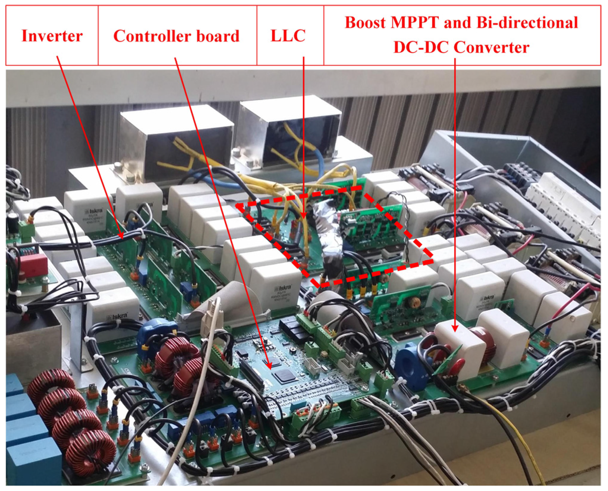
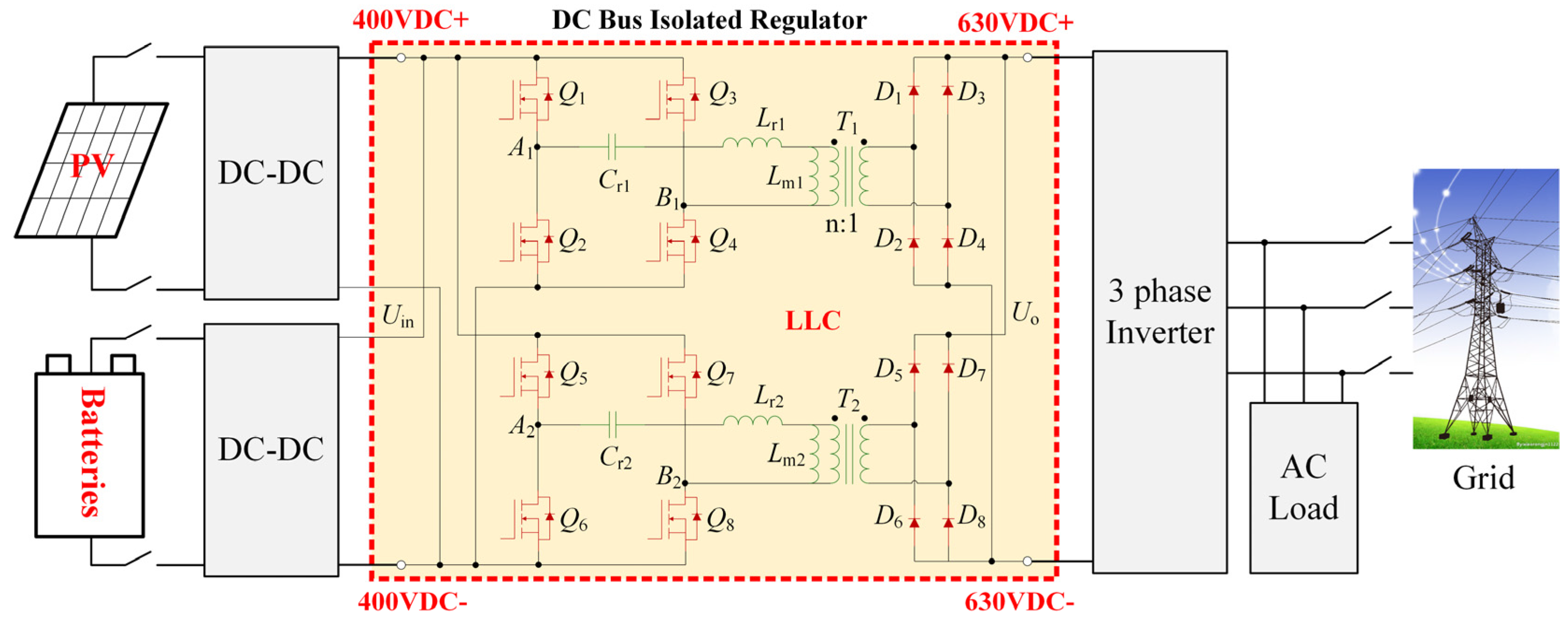
2.1. System Description

Figure 1 shows the architecture of a residential PV power system, which is composed of four parts. The boost maximum power point tracking (MPPT) converter and the bidirectional DC-DC converter transfer the energy from the PV and batteries to the 400 V DC bus. Compared to the systems placing batteries at the output of PV MPPT converter, the structure in this paper can easily control charging/discharging state and current of batteries with bidirectional DC/DC converter, which is benefit for the life time and usage cost of the batteries.
Following them, a parallel full-bridge LLC converter is connected to the next 630 V DC bus, which are used to supply high-frequency isolation and voltage regulation for the system. LLC converters guarantee electrical isolation with high working frequency. As its full-load efficiency is 98.4% and maximum efficiency is 98.7% in experiments, efficiency is not reduced largely when energy is transferred from PV and batteries to grid. At the end, a three-phase inverter is connected to the grid, which supplies the household load. The proposed residential PV power system can be operated in both on-line and off-line mode:
(1)
In on-line mode, the LLC converters control the 400 V DC bus voltage. The inverter regulates the 630 V DC bus and harmonics of the output currents. The boost converter adopts the MPPT algorithm. The bidirectional converter adopts current control to compensate the power difference between household load and PV.
(2)
In off-line mode, the LLC resonant converters control the 630 V DC bus voltage. The inverter regulates the AC output voltage. The boost converter adopts the MPPT algorithm and the bidirectional converter adopts voltage control to regulate the 400 V DC bus voltage.

2.2. Existing Problem Description

In the proposed residential PV system, the energy generated by PV is delivered to the batteries, little power is transmitted to inverter through the LLC resonant DC-DC converters, when the household load is light. The LLC converters may always work at light load condition. So the problem of the upturn of the LLC voltage gain at high frequencies given in [21] will be inescapable. According to experiments, the light load gain is so high that the required voltage (630 V DC or 400 V DC) cannot be restrained. Thus, the voltage regulation problem could be described as following:
(1)
In on-line mode, the 400 V DC bus voltage, U400, will be lower than 400 V, and a steady-state error exists, as the 630 V DC bus voltage is constant and regulated by the following inverter with closed-loop control.
(2)
In off-line mode, the 630 V DC bus voltage, U630, will be higher than 630 V normally. Burst mode is adopted, too large voltage ripple exists, as the 400 V DC bus voltage is stable and controlled by the bidirectional DC-DC converter, as shown in Figure 1.
(3)
Too slow voltage regulation when the load changes, and too large a voltage spike or sink when the load is changing suddenly.

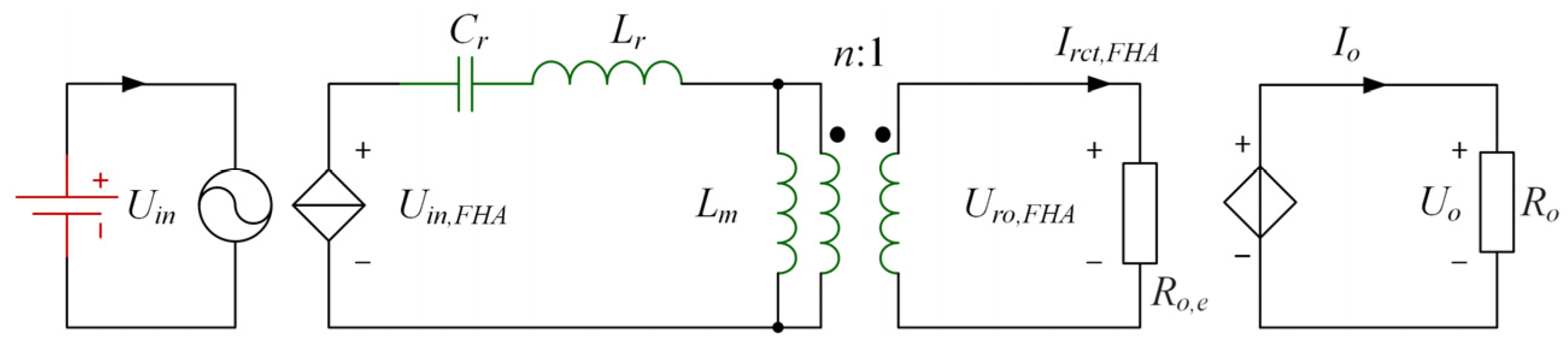
3. Ideal and Actual FHA Model

FHA modeling method is widely used due to its simple and effectiveness. In this paper, FHA modeling process is based on previous research [30,31] and we just used it to analyze and explain the difference between ideal and actual gain of the LLC converter.
Figure 1 shows the topology of the proposed full-bridge LLC resonant converter. The input voltage is Uin, the output voltage is Uo. The resonant tank is formed by the resonant capacitor Cr, the resonant inductor Lr and the magnetizing inductor Lm of the transformer. The turn ratio of the transformer is n:1. The switches on the primary side of the transformer (Q1, Q2, , and Q8) are MOSFETs. In the output rectifier, D1, D2, , and D8 are the rectifier diodes. The DC voltage gain in this paper refers to the ratio of output voltage: Uo/Uin.

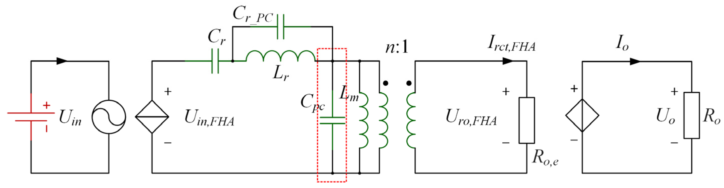
3.1. Ideal FHA Model Analysis

Firstly, several assumptions are made here:
(1)
Waveforms in resonant tank are perfect sinusoidal waves under any working frequency.
(2)
All the energy is conveyed by the fundamental component of the input voltage: uin,FHA.
(3)
All the parasitic parameters are neglected.
(4)
Figure 2 shows the ideal equivalent circuit of the proposed full-bridge LLC converter using the FHA modeling method [31].
As is known, LLC converter has two resonant frequencies, in this paper we define the higher resonant frequency fr1 as the main resonant frequency fr, that means: fr = fr1. fr2 is the secondary or lower resonant frequency:
f r 1 = 1 2 π L r C r   ,   f r 2 = 1 2 π ( L r + L m ) C r
and uin can be expressed with the Fourier series as:
u i n ( t ) = 4 U i n π N = 1 , 3 , 5 , 1 N sin ( 2 π N f t )
t is the time parameter, N is the integer parameter for the Fourier series expansion, and f is the switching frequency. According to the above assumptions, the input voltage of LLC resonant network can be regarded as its fundamental component, thus the fundamental component of uin is:
u i n , F H A ( t ) = 4 U i n π sin ( 2 π f t )
The root mean square (RMS) value of uin,FHA can be calculated as:
U i n , F H A ( t ) = 2 2 U i n π
Likewise, the output voltage of the resonant network, can be expressed as:
u r o ( t ) = 4 U o π N = 1 , 3 , 5 , 1 N sin ( 2 π N f t ϕ )
where φ is the time shift compared to the input voltage, and the fundamental component of uro is shown as:
u r o , F H A ( t ) = 4 U o π sin ( 2 π f t ϕ )
The RMS value of uro,FHA can be calculated as:
U r o , F H A = 2 2 U o π
The fundamental component of the rectifier current irct can be expressed as:
i r c t , F H A = 2 I r c t , F H A sin ( 2 π f t ϕ )
where Irct,FHA is the RMS value of irct,FHA.
Thus the average output current Io can be obtained:
I o = 2 T s 0 T 2 | i r c t , F H A ( t ) | d t = 2 2 π I r c t , F H A
and the equivalent output resistance of the resonant network can be expressed as follows:
R o , e = U r o , F H A I r c t , F H A = 2 2 π U o π 2 2 I o = 8 π 2 R o
In order to simplify the calculation, the equivalent output resistance in the secondary side of the transformer can be converted to the primary side:
R o , e = n 2 R o , e
With all the given parameters, φ can be calculated as:
ϕ = arctan [ 2 π f L m n 4 R o , e 2 + ( 2 π f L r 1 2 π f C r ) ( n 4 R o , e 2 + 4 π 2 f 2 L m 2 ) 4 π 2 f 2 L m 2 n 2 R o , e ]
The forward transfer function of the resonant network can be derived as follows:
H ( s ) = U o , F H A ( s ) U i n , F H A ( s ) = s L m R o , e n [ ( s L m + R o , e ) ( s L r + 1 s C r ) + s L m R o , e ]
Finally, the ideal voltage gain of the LLC resonant converter can be calculated as:
G i d = U o U i n = U o , F H A U i n , F H A = H ( j 2 π f ) = ( j 2 π f ) 2 L m C r R o , e n ( R o , e ( j 2 π f ) 2 L r C r R o , e ( j 2 π f ) 2 L m C r R o , e ) 2 + ( ( j 2 π f ) L m ( j 2 π f ) 3 L m L r C r ) 2

3.2. Actual FHA Model Analysis Including Parasitic Capacitors

In order to illustrate the upwarp drifting of the voltage gain curve, the junction capacitances of the rectifier diodes and the wiring capacitance of the transformer are added. Its equivalent FHA circuit is shown in Figure 3. Cpc represents the total parasitic capacitances of the rectifier diodes and transformer windings. Cr_PC represents parasitic capacitance of resonant inductor, which has not been considered in former work [21]. In our LLC converter, Cr_PC = 0.2 nF. Cr_PC is so small, and the impact of the parameter of Cr_PC can be neglected, so the parameter will not appear in the actual FHA model and analysis in the whole article. From Figure 3, it can be obtained that the reason of the upwarp drifting should be ascribed to the high order resonance between the resonant tank and parasitic capacitors Cpc.
After considering Cpc, the voltage gain of LLC converter can be rewritten as:
G p c = R o , e 2 π f C r B ( f ) n [ A ( f ) B ( f ) ] 2 + { R o , e [ A ( f ) 2 π f C p c + B ( f ) 2 π f C r ] } 2
where A(f) and B(f) are defined as:
A ( f ) = 4 π 2 f 2 L r C r 1
B ( f ) = 4 π 2 f 2 L m C p c 1
As shown in Figure 4, the full line is the gain curve considering parasitic parameters with (15), the dash line is the ideal gain curve. The straight dot dashed line is the expected voltage gain (630 V DC/400 V DC = 1.575). Those curves are given under the same output resistance (5 kΩ), and fr is 78.8 kHz. Therefore, the expected voltage gain cannot be obtained under the model considering actual parasitic parameters, which is the same as the experimental result.

4. New Control Method at Light Load Conditions

As shown in Figure 3, there is an additional Cpc in the actual FHA model, which is parallel with the transformer. Therefore, the reason of upwarp drifting of the voltage gain curve can be ascribed to the higher-order resonance between resonant tank and parasitic capacitors, and there is an additional resonant bottom where the frequency is higher than the main resonant frequency fr in Figure 4. But it is hard to calculate the real value of Cpc due to the uncertainty of parasitic parameters.
In order to solve this non-monotonic problem simply and effectively, this paper presents a changing topological control method. By adapting PFM driver signals, the full-bridge LLC converter can be changed into half-bridge LLC, and the voltage gain could be reduced by half.

4.1. Proposed Changing Topological Control Method

As shown in Figure 5, a full-bridge LLC can be simply transformed into a half-bridge LLC by turning off Q3 and turning on Q4 (as shown in Figure 1) incessantly. The input voltage of resonant tank in full-bridge LLC, uAB_F, ranges from Uin to −Uin in one period, each voltage lasts 50% of the whole period, but that in half-bridge LLC, uAB_H, ranges from Uin to 0 in one period, each voltage lasts 50% of the whole period. Thus, the RMS value of fundamental harmonic of uAB_F in full-bridge LLC, UAB_F, can be displayed as:
U A B _ F = 0 1 / f u A B _ F d t 1 / f = 2 2 π U i n
And the RMS value of fundamental harmonic of uAB_H in half-bridge LLC, UAB_H, can be displayed as:
U A B _ H = 0 1 / f u A B _ H d t 1 / f = 2 π U i n = 1 2 U A B _ F
By adopting (10), (11) and (15), we can conclude that given the same output resistance Ro, the voltage gain of the half-bridge LLC mode GH_pc is half of that of the full-bridge mode:
G H _ p c ( f , R o ) = 1 2 G p c ( f , R o )
To verify the above analysis, an open loop experimental based on a half-bridge LLC converter has been carried out. As shown in Figure 6, the solid line is the voltage gain curve calculated by the actual FHA model with (15), and the dashed line is the experimental results, which are obtained by changing the operating frequency under the same input voltage and output resistance (5 kΩ), and fr is 78.8 kHz. The straight dot dashed line (the same with Figure 4) is the expected voltage gain. Therefore, by utilizing the proposed changing topological control method, the expected voltage gain can be obtained under very light load condition, and even the switching frequency could be reduced.
Compared to the full-bridge LLC, conduction loss and core loss in the half-bridge LLC increases due to the larger RMS of the resonant current. As the switching frequency becomes lower, and MOSFETs in switching mode decrease from 4 to 2, the turn-off loss declines largely. To conclude, at light load condition, the fall of turn-off loss is larger than the rise of conduction loss and core loss. Overall, the efficiency under half-bridge mode is a little higher than that under full-bridge mode.

4.2. Design Consideration Based on the New Method

As is discussed above, to track the required gain of the LLC converter in all load range, it is important to find the required gain in full-bridge mode when load is normal. It is also important to find the required gain in half-bridge mode when load is light, so there are several restrictions. In the following Section 4.2.1, the design procedure of the resonant tank parameters and power devices will be discussed. The requirement and design approach of the voltage gain and working frequency range for the changing topological LLC converter, which are used to meet the voltage gain requirements of the whole load range, will be analyzed in Section 4.2.2.

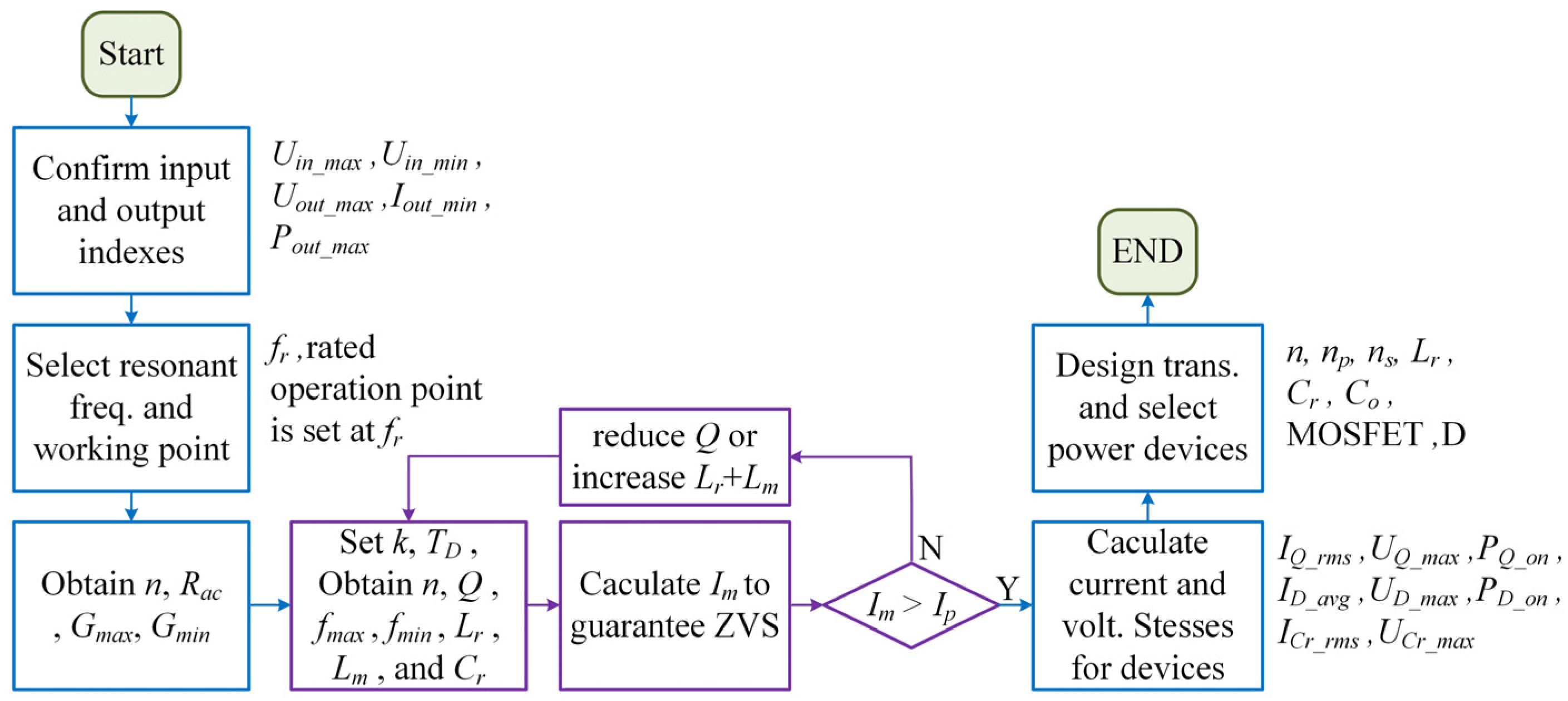
4.2.1. Resonant Parameters and Rated Operationg Point Design

In this paper, the design procedure of the resonant tank parameters and power devices which is presented in [31] will be adopted. As shown in Figure 7, Uin_max, Uin_min, Uout_max and Uout_min are the maximum and minimum of input and output voltage respectively, Pout_max is the maximum output power, n, np, ns, Lr, Lm is the turn ratio, turns of primary and secondary, resonant inductor and excitation inductor of the transformer respectively, Cr is the resonant capacitor, Co is the output filter capacitor, Rac is the effective resistive load reflected to the primary side, Gmax and Gmin are the required maximum and minimum voltage gain under full-bridge LLC topology, k is the ratio of Lm to Lr, TD is the dead-time of the bridge-arms, Q is the quality factor of the resonant tank, fmax and fmin is the feasible maximum and minimum operating frequency under different load conditions, Ip is the current in the resonant tank, Im is the excitation current of the transformer, IQ_RMS, UQ_max and PQ_max are the maximum RMS current, drain-source voltage and loss power of each MOSFET respectively, ID_avg, UD_max, PD_on are the maximum average current, inverse voltage and loss power of each rectifier diode respectively, Icr_RMS and UCr_max are the maximum RMS current and peak resonant voltage of Cr.
The design and optimization method is based on full-bridge LLC topology, because the efficiency of normal load range, for example 10–100%, is the main optimization objective and the main operating conditions. On the other hand, the main resonant frequency fr (or fr1) and rated steady state working frequency are preset. The common setting of fr is 100 kHz, in this paper, the output power per channel is up to 4 kW, so in order to strike a balance between power efficiency and power density, the setting of fr will be nearly 80 kHz.
The rated steady state working frequency setting needs to consider the limited peak voltage gain under 4 kW output condition, large DC bus voltage fluctuations caused by the transient procedures and rated conversion efficiency comprehensively.
As the rated power is 4 kW in each channel, it is hard to get a high voltage gain as in [28], because the equivalent resistance Ro is too small to make the curve goes up. Thus, the peak voltage gain should be guaranteed to regulate two DC bus voltage during a large disturbance.
The problem of gain upturn could be avoided by using the proposed changing topological control method, so the limited voltage gain problem should be considered during rated operating point presetting. Therefore, the rated gain can be achieved slightly above the main resonant frequency fr, making full use of drop scope of gain curve. It can guarantee a wider gain range and higher efficiency near operation point.

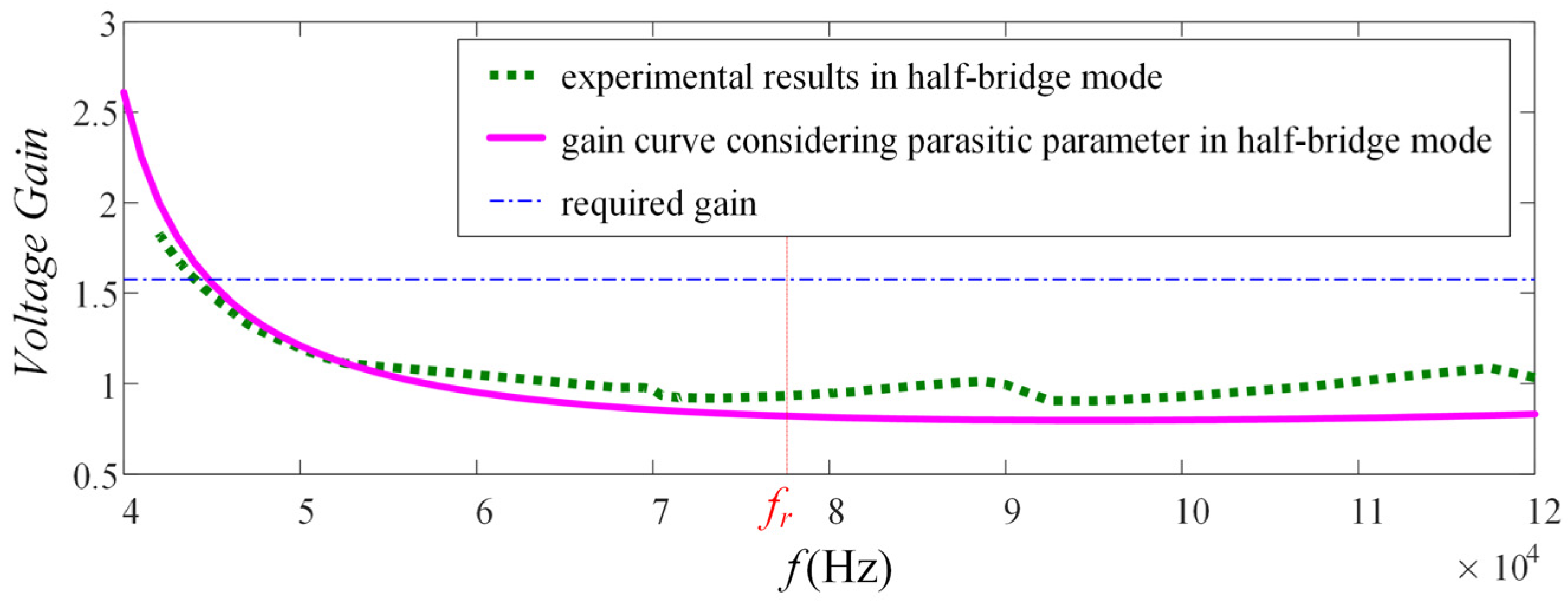
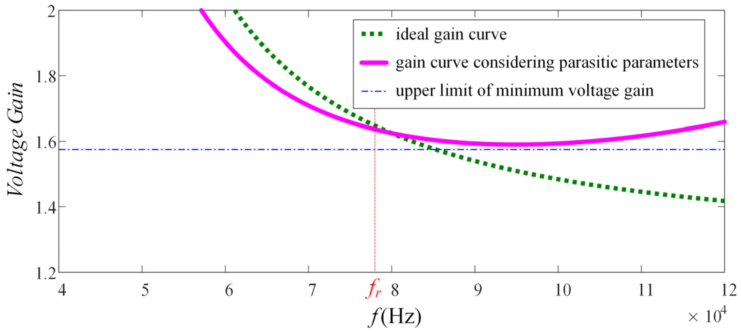
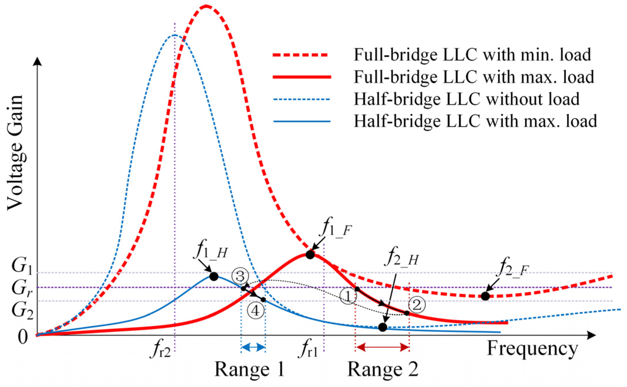
4.2.2. Voltage Gain and Working Frequency Range Selection

By using the proposed changing topological control method and the design procedure discussed in Section 4.2.1, the voltage gain and working frequency range selection are illustrated in Figure 8. When the LLC operates in full-bridge LLC mode, f1-F is the voltage gain peak point under maximum load condition, for example 4.8 kW (1.2 times of rated power), f2-F is the minimum voltage gain point under selectable minimum load, for example 0.8 kW (0.2 times of rated power). When the load is reduced continuously, the circuit will be changed into half-bridge LLC, f1-H is the voltage gain peak point under maximum selectable load condition in half-bridge mode, for example 1.2 kW (0.3 times of rated power), f2-H is the minimum voltage gain point without load. Therefore, within range 2, point 1 is the minimum frequency point and point 2 is the maximum frequency point under full-bridge LLC topology, and within range 1, point 3 is the minimum frequency point and point 4 is the maximum frequency point under half-bridge LLC topology.
It is necessary to calculate the feasible minimum and maximum frequency, to select the operating frequency range and to ensure a suitable gain can be attained, in which the gain curve is monotonic without upturn.
The first-order derivative of the half-bridge LLC voltage gain can be described as:
G H _ p c ( f 1 _ H , R o , C p c ) = R o , e C r ( 12 π 2 f 2 L m C p c 1 ) [ C ( f ) 2 + D ( f ) 2 ] 2 n [ C ( f ) 2 + D ( f ) 2 ] 3 2 R o , e C r π f B ( f ) C ( f ) [ 6 π f L m C p c A ( f ) + 6 π f L r C r B ( f ) ] n [ C ( f ) 2 + D ( f ) 2 ] 3 2 R o , e 2 C r π f B ( f ) D ( f ) ( 12 π 2 f 2 L r C r C p c + 12 π 2 f 2 L m C r C p c ) n [ C ( f ) 2 + D ( f ) 2 ] 3 2 + R o , e 2 C r π f B ( f ) D ( f ) ( C p c + C r ) n [ C ( f ) 2 + D ( f ) 2 ] 3 2
C(f) and D(f) are defined as:
C ( f ) = A ( f ) B ( f )
D ( f ) = 2 π f R o , e [ C p c A ( f ) + C r B ( f ) ]
By making GH_pc zero, extreme points of GH_pc are obtained. f1_H is a local maximum value point, and f2_H is a local minimum value point. As shown in Figure 8, the frequency range between f1_H and f2_H is the maximum feasible working area for the half-bridge LLC resonant converter, and range 1 should be contained within f1_H and f2_H. Similarly, the frequency range between f1_F and f2_F is the maximum suitable working area for the full-bridge LLC resonant converter, and range 2 should be contained within f1_F and f2_F.
In Figure 8, if Gr declines to the position of G2, the required gain cannot be tracked with the full-bridge LLC converter. Taking a margin of 0.1Gr into consideration, the selection of load or Ro should satisfy the following equation:
G p c ( f 2 _ F , R o , C p c ) 0.9 G r
The gain of the local maximum point f1_F, should be larger than the required gain. Taking a margin of 0.2Gr into consideration:
G p c ( f 1 _ F , R o , C p c ) 1.2 G r
In half-bridge mode, the gain of the local maximum point f1_H, should be larger than the required gain Gr. If Gr rises to the position of G1, the required gain cannot be tracked with the half-bridge LLC converter. Taking a margin of 0.1Gr into consideration, the selection of Ro should satisfy the following equation:
G H _ p c ( f 1 _ H , R o , C p c ) 1.1 G r
The gain of the local minimum point f2_H should be smaller than the required gain Gr. Taking a margin of 0.2Gr into consideration:
G H _ p c ( f 2 _ H , R o , C p c ) 0.8 G r
Considering the above design method and optimization factors, resonant tank parameters, the voltage gain and frequency range could be calculated.
Furthermore, in order to realize fast dynamic response and good steady performance within the whole load conditions, a new DC bus voltage control and current sharing strategy is proposed for the parallel LLC resonant converter. By ensuring that the LLC works in full-bridge mode with normal load and in half-bridge mode with light load, the DC bus voltage is controllable in all load range. Meanwhile, with a dead-band controller, two resonant inductor currents can be shared evenly. The following Section 5 will discuss the proposed control method under on-line mode and off-line mode separately, and corresponding simulation results will be given.

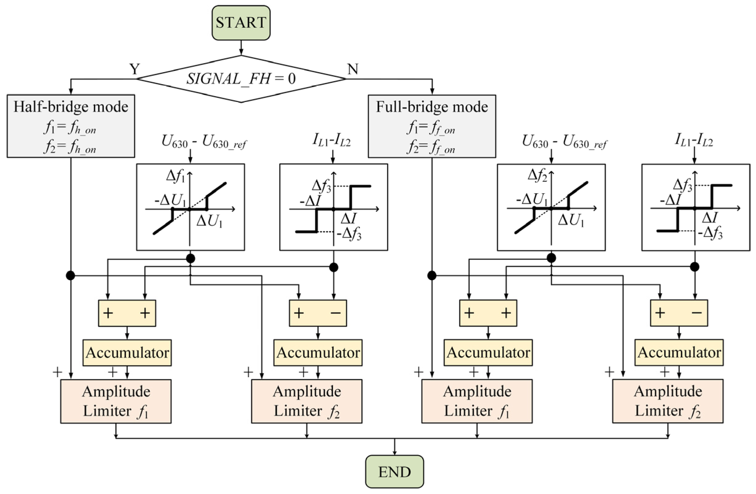
5. Control of the Variable Structure LLC Converter

As shown in Figure 9, a hysteresis controller is proposed to transform the mode of the proposed LLC converter. Pinv is the output power of the inverter, it is equal to the output power of LLC converter when power loss of the inverter is ignored. PU is the minimum load for the full-bridge LLC converter, and PL is the maximum load for the half-bridge LLC converter.
If the output power of inverter is above PU, LLC converter operates in the full-bridge mode. If the output power of inverter is below PL, LLC converter operates in half-bridge mode. Otherwise, the mode stays the same. Furthermore, PL is a little smaller than PU, in order to avoid continuous power fluctuations around the transition gap.

5.1. Proposed Control Scheme in on-Line Mode

As illustrated in Figure 10, U400_ref is the reference of the 400 V DC bus voltage, IL1 and IL2 are the resonant inductor RMS currents of each channel, f1 and f2 are the working frequencies of each channel.
When SIGNAL_FH is 0, the converter is transformed into half-bridge mode. The frequency of two LLC resonant converters start to change on the basis of fh_on. Then a dead band controller is used to control the 400 V DC bus voltage. If the 400 V DC bus voltage U400 is lower than (U400_ref − ΔU1), the frequencies are increased by Δf1, to attain lower gain and higher 400 V DC bus voltage. If U400 is higher than (U400_ref + ΔU1), the frequencies are altered by Δf1, to attain higher gain and lower voltage. In this paper Δf1 is defined as:
Δ f 1 = { k 1 ( U 400 U 400 _ r e f )        | U 400 U 400 _ r e f | Δ U 1 0                                                        ​​​​​ ​​    | U 400 U 400 _ r e f | < Δ U 1
When SIGNAL_FH is 1, the gate signals of Q3 and Q4 return to normal. The LLC resonant converter operates in full-bridge mode with an initial frequency of ff_on. The controller is similar; the difference is that the step of the dead-band control scheme of DC bus voltage is Δf2:
Δ f 2 = { k 2 ( U 400 U 400 _ r e f )        | U 400 U 400 _ r e f | Δ U 1 0                                                         ​​    | U 400 U 400 _ r e f | < Δ U 1
k1 and k2 are constant, they are selected by considering the fast response and stability requirements.
Simultaneously, another dead-band controller works to balance the two LLC currents. In Figure 10, the step of Δf3 is constant and in fact very small, so the allowable error scope ΔI is 0.02|IL1IL2|. If resonant inductor RMS current of first channel LLC is bigger than that of second channel LLC, and the error is over ΔI, working frequency of first channel LLC is increased by Δf3 and working frequency of second channel LLC is decreased by Δf3. On the contrary, the working frequency of first channel LLC is decreased by Δf3 and the working frequency of second channel LLC is increased by Δf3 Otherwise, when the error between two RMS currents is over −ΔI and below ΔI, which means two resonant currents are almost balanced, this dead band controller of current sharing doesn’t work. By use of fixed step of Δf3 in dead band controller, resonant currents may not be exactly the same. However, in practical application RMS values of resonant currents need not to be identical. Also, the dead band controller is simple and can make LLC converter more stable.

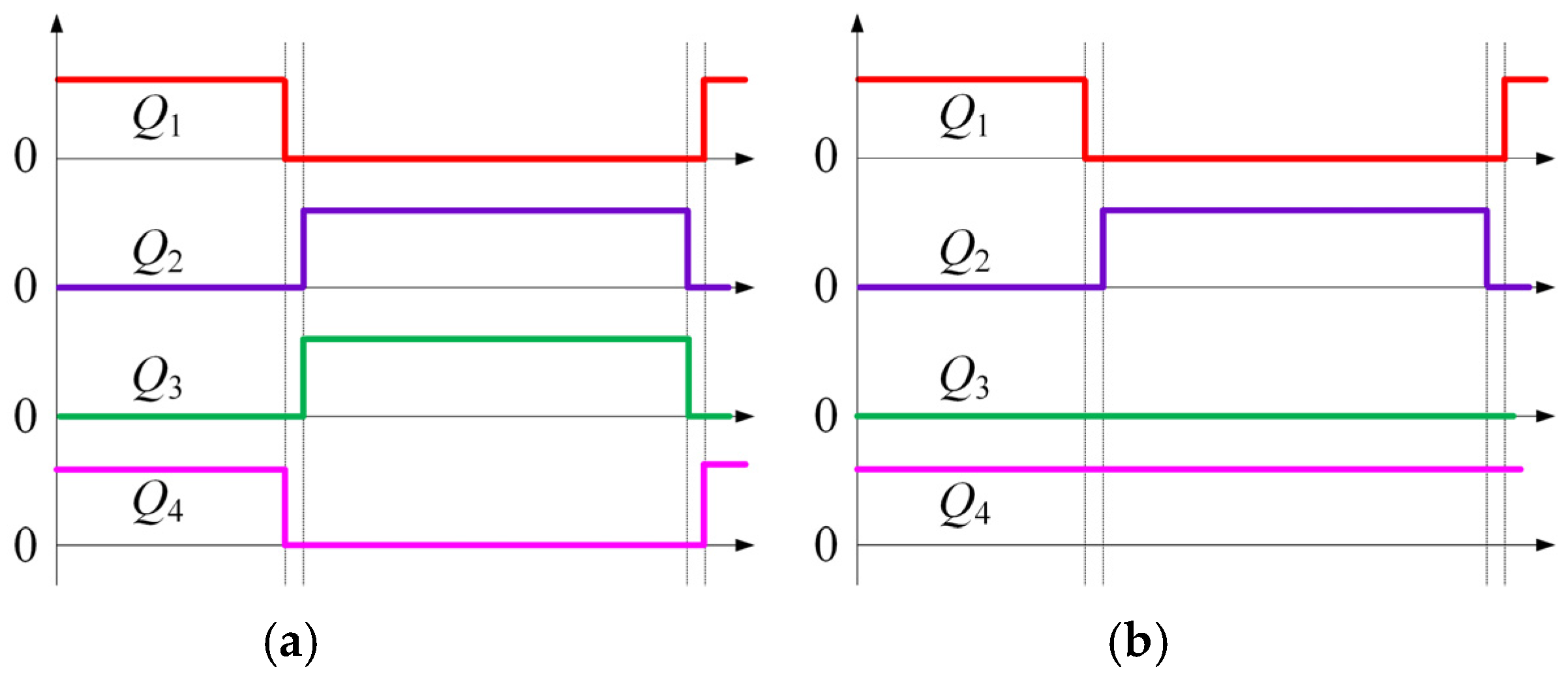
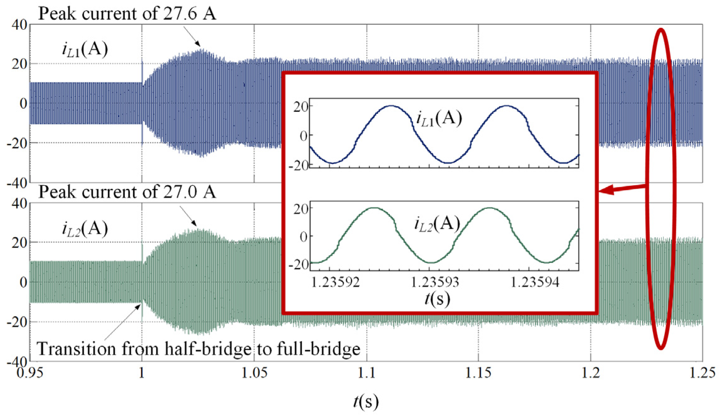
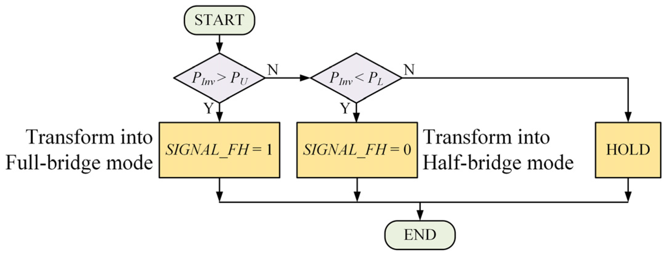
5.1.1. Transfer Conditions between Half-Bridge and Full-Bridge Mode

Assuming the efficiency of inverter is η, the output voltage of LLC converters is U630_ref, the equivalent output resistance for each LLC, RP could be expressed as:
R P = 2 U 2 630 _ r e f η P i n v
According to load range selection criteria, to make sure that the transition between half-bridge and full-bridge mode is smooth, the LLC output resistance should satisfy Equations (24)–(27), that means:
{ max { R 1 _ H , R 1 _ F }     2 U 2 630 _ r e f η P L   min { R 2 _ H , R 2 _ F } max { R 1 _ H , R 1 _ F }   2 U 2 630 _ r e f η P U      min { R 2 _ H , R 2 _ F }
where R1_F, R1_H are the minimum solutions to (25) and (26), and R2_F, R2_H are the maximum solution to (24) and (27). The selection of PL and PU should meet (31).

5.1.2. Initial Working Frequency Selection

At beginning of each working mode (full-bridge or half-bridge mode), a proper initial operating frequency is necessary to get a smooth transition performance. As is shown in Figure 10, when the converter changes from half-bridge mode to full-bridge mode, the initial frequency ff_on is the solution to the following equation:
G p c ( f f _ o n , 2 U 2 630 _ r e f P i n v _ r a t e , C p c ) = G r
Pinv_rate is the rated output power of the inverter, and 2(U630_ref)2/Pinv_rate is the corresponding equivalent output resistance of each LLC. When the converter changes from full-bridge mode to half-bridge mode, the initial frequency fh_on could be calculated as:
G H _ p c ( f h _ o n , 2 U 2 630 _ r e f P L , C p c ) = G r

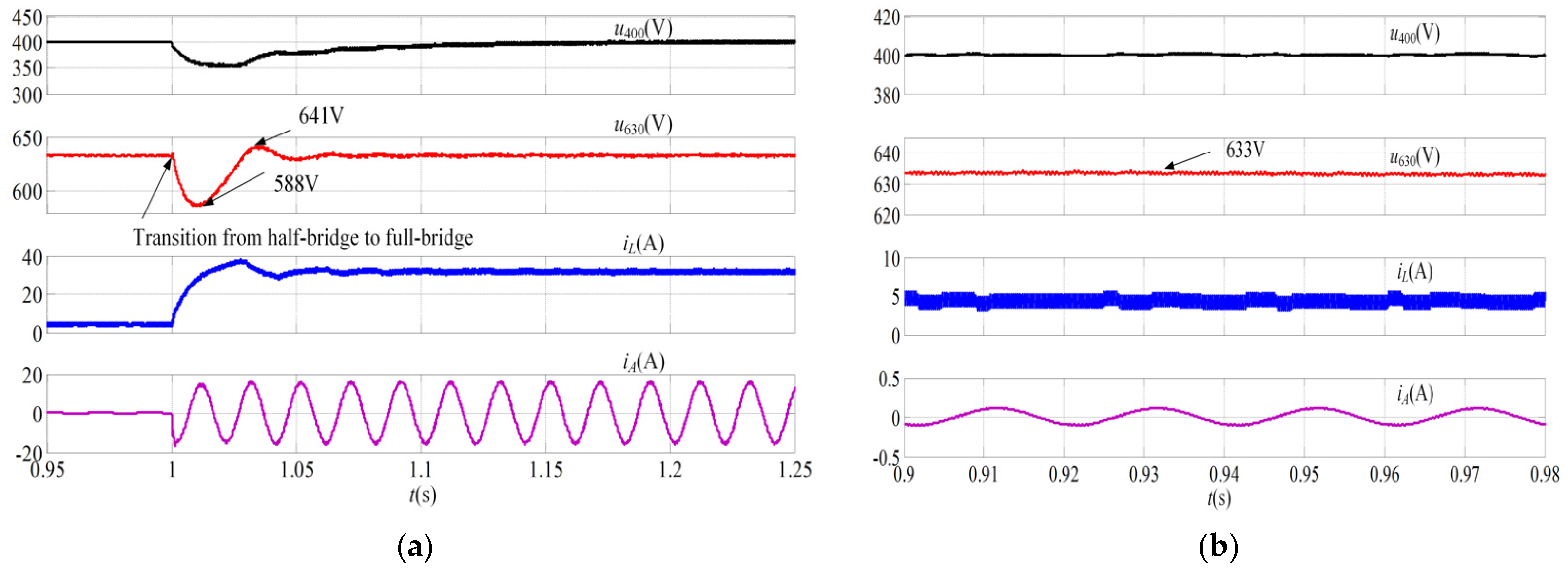
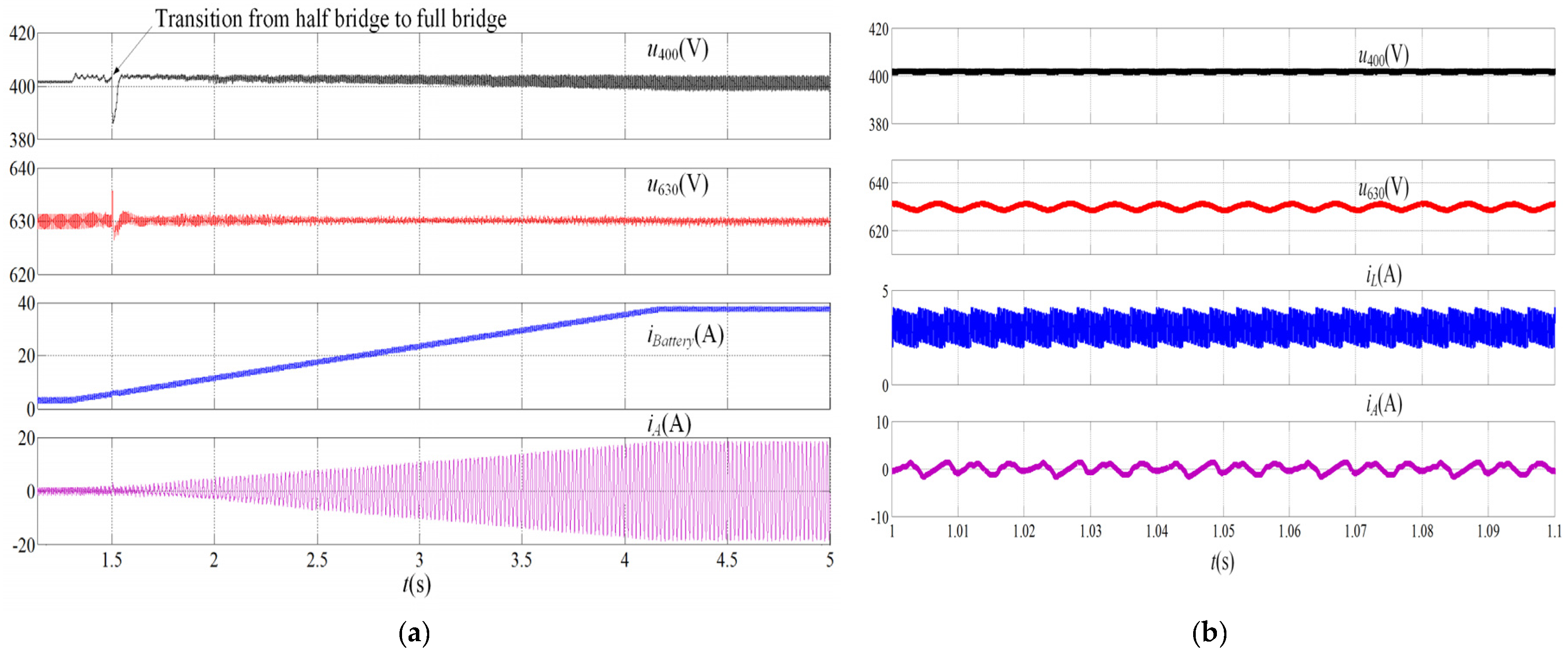
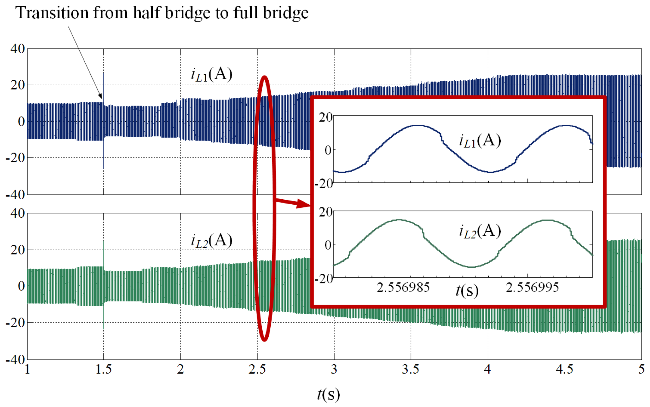
5.2. Simulation Results in On-Line Mode

In order to verify the proposed design scheme, a simulation model is fulfilled in MATLAB. The main simulation parameters are listed in Table 1. To simplify the model and shorten the running time of simulation, only battery is used as source here. To verify the proposed current sharing strategy, the different resonant tank parameters of two channels are given deliberately.
To describe the current sharing result, a parameter named current unbalance factor (CUF) is given, which can be defined as absolute value of error between two resonant RMS currents divided by average value of two resonant RMS currents. CUF = |2(IL1IL2)/( IL1 + IL2)|.
The simulation results in on-line mode are shown in Figure 11. iBattery is the current of battery, iA is inverter output current of phase A. u400, u630 are the same as 400 V DC bus voltage U400 and 630 V DC bus voltage U630, but u400, u630 represent instantaneous values in this article. According to the control scheme, u400 is controlled by LLC converters, and u630 is controlled by the inverter.
In Figure 11a, the reference of the battery current is 3 A before 1.3 s, and the two LLC resonant converters operate in half-bridge mode. The 400 V DC bus voltage is regulated with no ripple. At 1.3 s, the reference of battery current increases by 12 A/s, so the output currents of the inverter increase accordingly. At 1.5 s, the LLC resonant converters begin to operate in full-bridge mode, and their frequencies are set to ff_on. During this transition, the 400 V DC bus voltage recovers quickly, and the minimum voltage during the transition is 386 V. After approximately 3 s, the reference of the battery current arrives at 37.5 A, and remains unchanged. The entire system is stable and the 400 V DC bus voltage is flat during this period. Figure 11b shows the steady state simulation results at light load condition (half bridge mode), and the 400 V DC bus voltage is stable.
Figure 12 shows the current sharing results of LLC resonant converters with 0 to 7 kW load in on-line mode. At 1.5 s, half-bridge LLC transforms into full-bridge LLC. The figure in inner box shows detailed current waveforms around 2.55 s. It proves that two full-bridge LLC converters work with working frequencies above the main resonant frequency fr. This is because the required gain is achieved slightly above fr, making full use of drop scope of gain curve, as the last paragraph in Section 4.2.1 shows. The RMS values of two LLC resonant currents are both 9.6 A in the box, CUF is almost 0. The result indicates that in on-line mode, the proposed current sharing method can balance currents at light and full load condition, even during load transition process.

5.3. Proposed Control Scheme in Off-Line Mode

In off-line mode, the DC bus voltage control and current sharing strategy of the LLC resonant converter is similar to the strategy in on-line mode, but the DC bus voltage which is controlled by the LLC resonant converters is the 630 V DC bus voltage U630, and the 400 V DC bus voltage U400 is controlled by the forestage storage charge and discharge management converter. The architecture in Figure 13 and parameters of the entire simulation model are similar with on-line mode, so the details are not given here repeatedly.

5.4. Simulation Results in Off-Line Mode

In Figure 14a, prior to 1 s, AC load is 50 W, and LLC converter works in half-bridge mode. The 630 V DC bus voltage is regulated with no ripple. At 1 s, the AC load changes to 7 kW, so the LLC resonant converter begins to work in full-bridge mode, and frequency is set initially. During this transition, the 630 V DC bus voltage recovers in 50 ms, the settling time is 24 ms, the minimum voltage during the transition is 586 V, and the maximum voltage is 641 V. The entire system is stable during the transition. Figure 14b shows the simulation results at light load condition (half bridge mode). 630 V DC bus voltage is regulated smoothly.
Figure 15 shows the current sharing results of LLC resonant converters during load transition from 0 to 7 kW in off-line mode. The peak values of two resonant currents are 27.6 A and 27.0 A as Figure 15 shows. The figure in inner box shows detailed current waveforms around 1.23 s. RMS values of two LLC resonant currents are 11.8 A with 7 kW load. The results indicate that the proposed scheme can divide currents evenly during transition and at full load condition.

6. Experimental Results

The proposed control scheme of the full-bridge LLC converters is verified in a 7 kW residential PV system. Figure 16 shows the prototype system.
Design criteria and key components are listed in Table 2.
The PV arrays are replaced by a chroma62150H-1000S programmable DC power supply (Chroma, Taoyuan, Taiwan) with PV simulator. The maximum output power of the PV array simulator is 3.5 kW. The comparison between original waveforms and the optimization waveforms after using proposed control method is also discussed. Furthermore, in order to verify the availability of the proposed control method under real household loads such as air conditioner, microwave and refrigerator, experiments with real household loads are carried out.

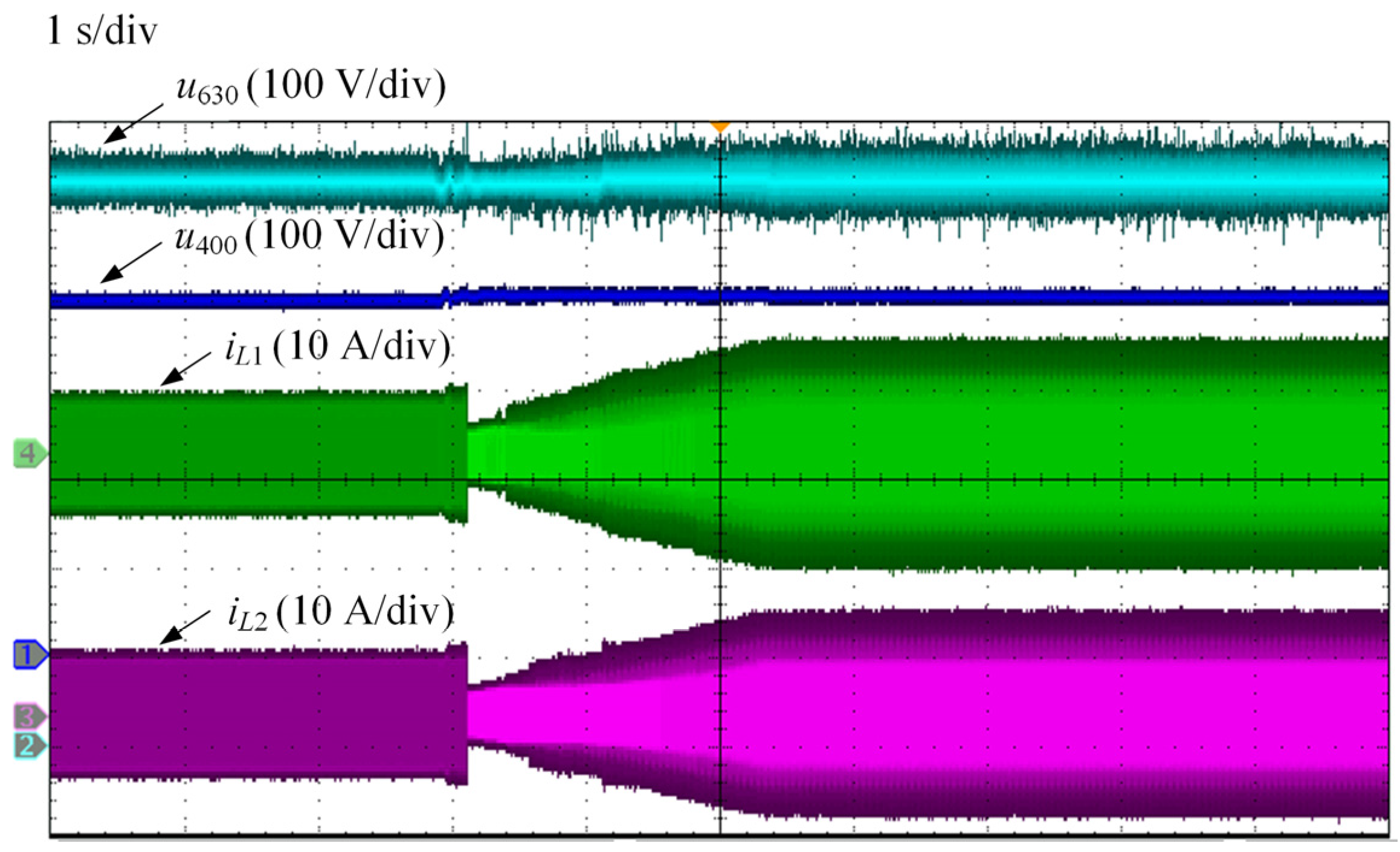
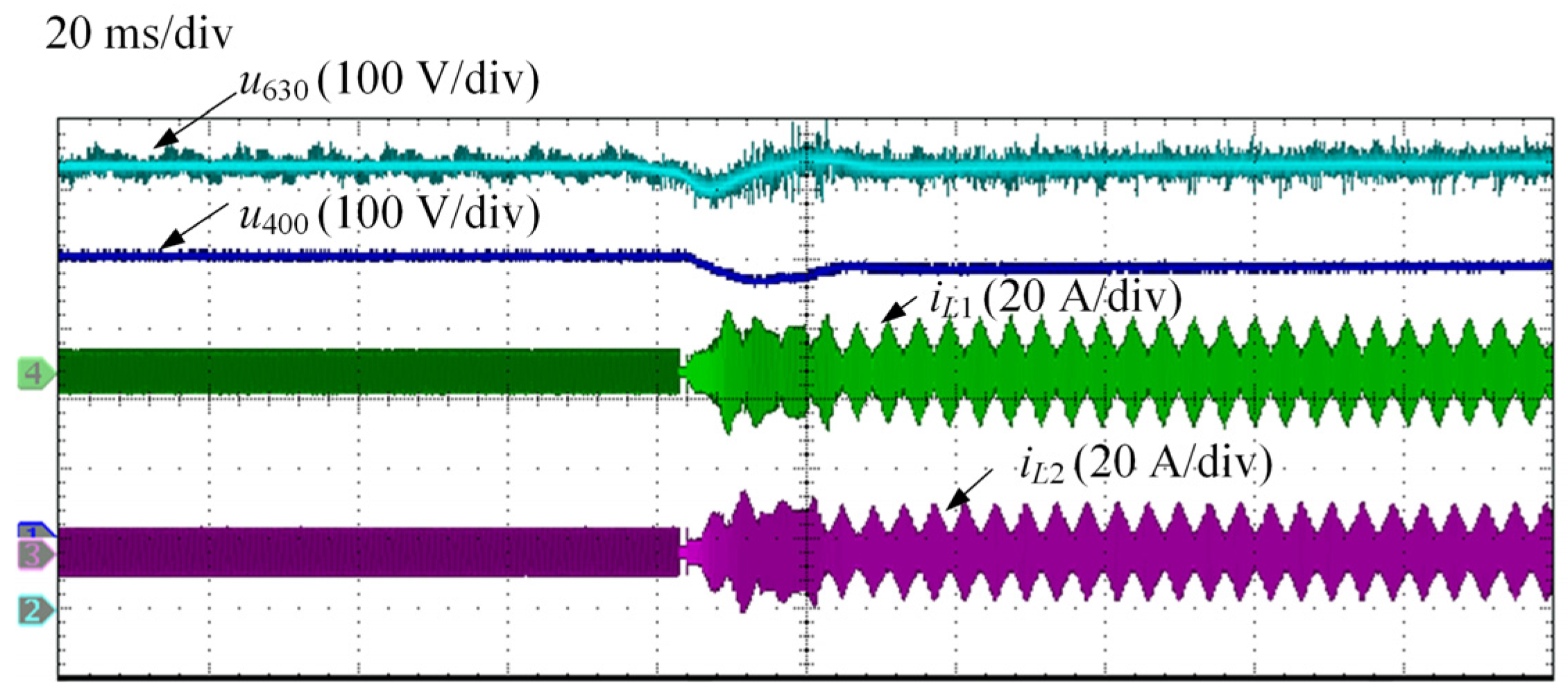
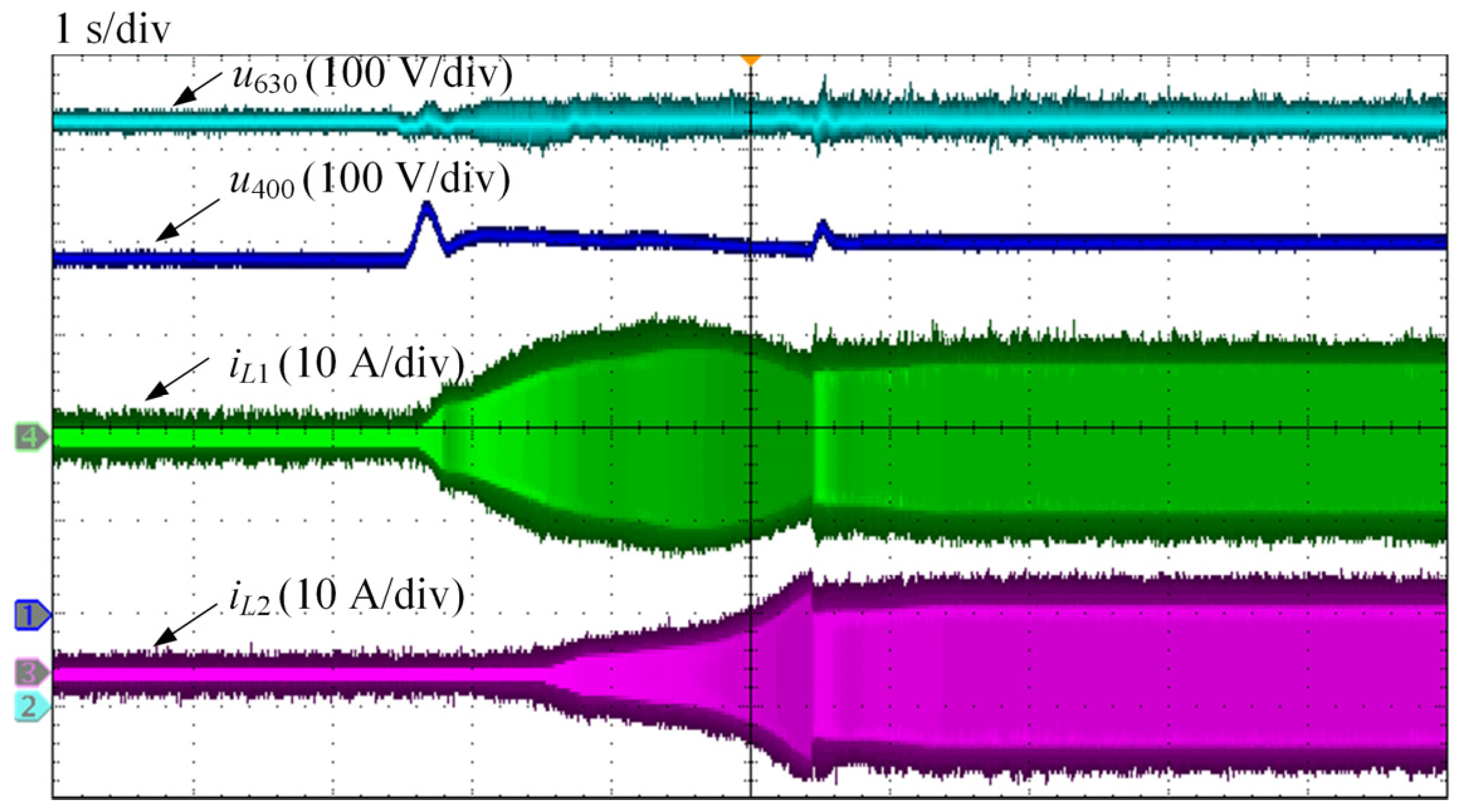
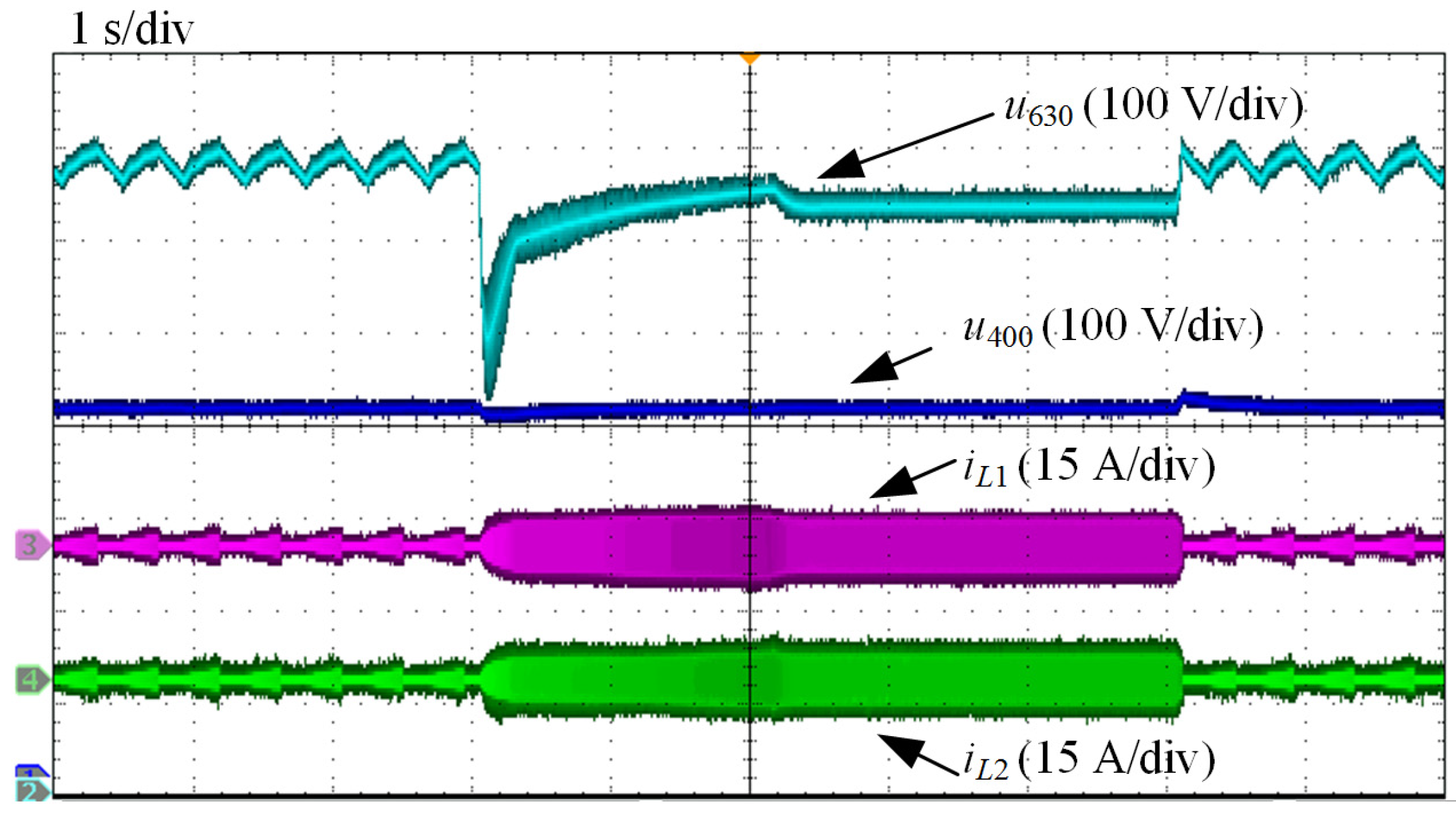
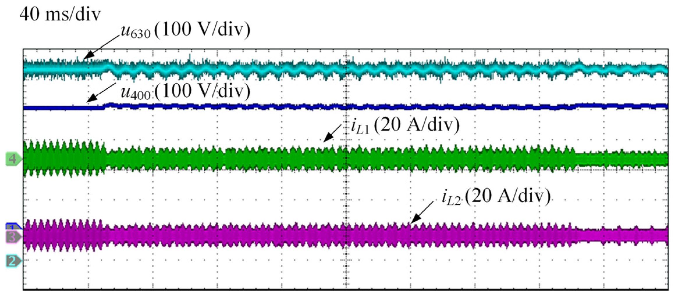
6.1. Experimental Results in On-Line Mode

In this mode, the control object is u400. Figure 17 shows the experimental results with the original control method in on-line mode. A steady-state error of −25 V exists in u400. After increasing the load from 0 to 7 kW, there is a pulse of 437 V and fluctuation during transition. The settling time is about 0.35 s. The current balance is out of control during transition process.
Figure 18 and Figure 19 show the experimental results with proposed control scheme in on-line mode. In Figure 18, during the transition of the LLC converters from 0 to 7 kW, the fluctuation of 400 V DC bus voltage is only −14 V, and the settling time can be neglected. The currents of the two LLC resonant inductors are shared evenly at last, with RMS of 12.2 A and 12.0 A. The CUF is about 1.7%.
Figure 19 shows a similar result when the AC load decreases from 7 kW to 0. For 400 V DC bus voltage, the maximum voltage drop is 18 V and the peak value is 422 V. What needs illustration is that u630 is controlled by inverter and the control method is not optimized. As space is limited, although the fluctuation of u630 is a little large, we will not discuss this problem here.

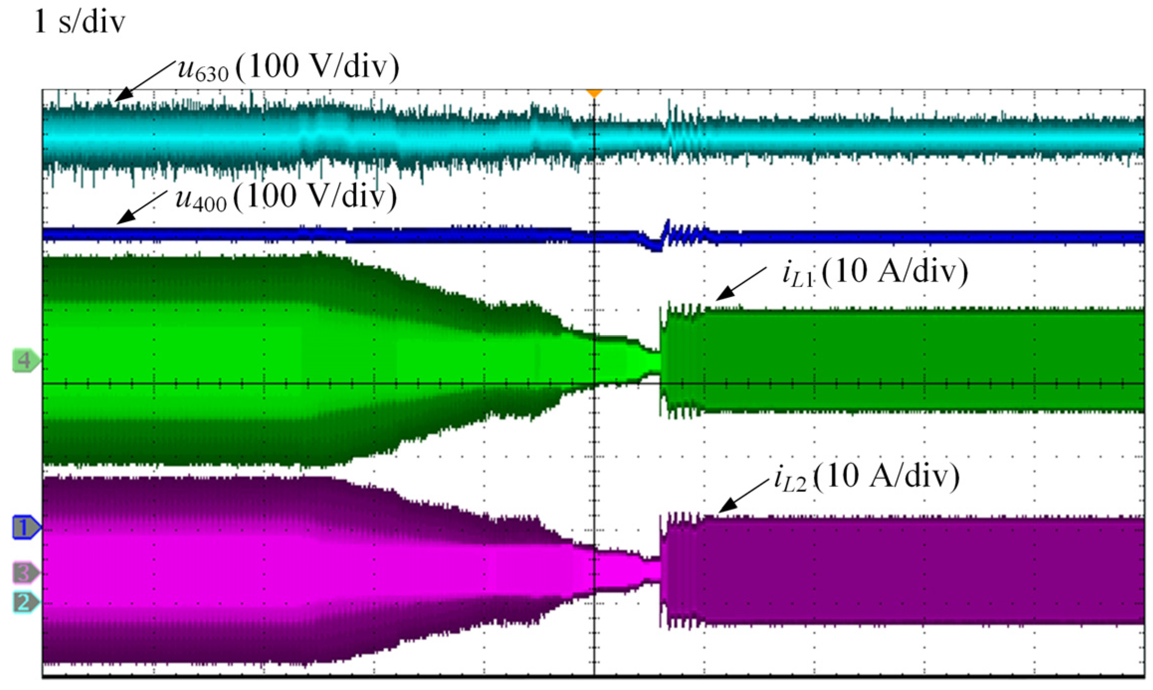
6.2. Experimental Results in Off-Line Mode

In this mode, the control object of LLC is u630. Figure 20 shows experimental results with the original control method in off-line mode. At no load condition, the controller works in burst mode. The voltage ripple is about 50 V, and the peak value is about 693 V. During the transition from 0 to 7 kW, in the worst case, the maximum voltage drop is about 211 V. The settling time is 0.63 s.
Figure 21 and Figure 22 show the experimental results with the proposed control method in off-line mode. As shown in Figure 21, when AC load increases from 0 to 7 kW, with the proposed control scheme, the 630 V DC bus voltage declines to 589 V during the transition and recovers after 21 ms. The peak voltage is 642 V. The maximum CUF is about 0.7%. The experimental results are in consistent with simulation results. Figure 22 shows the experimental waveforms with AC load variation from 7 kW to 2.3 kW to 0. The 630 V DC bus voltage fluctuation is only about 10 V during transition.

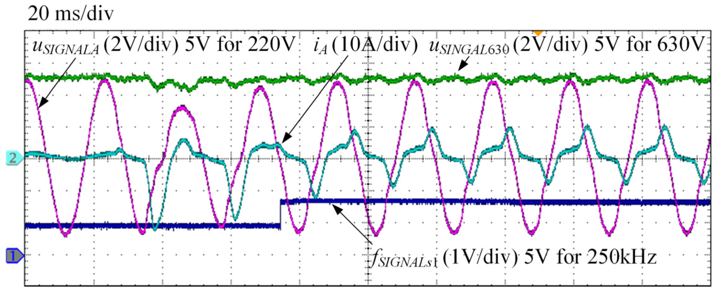
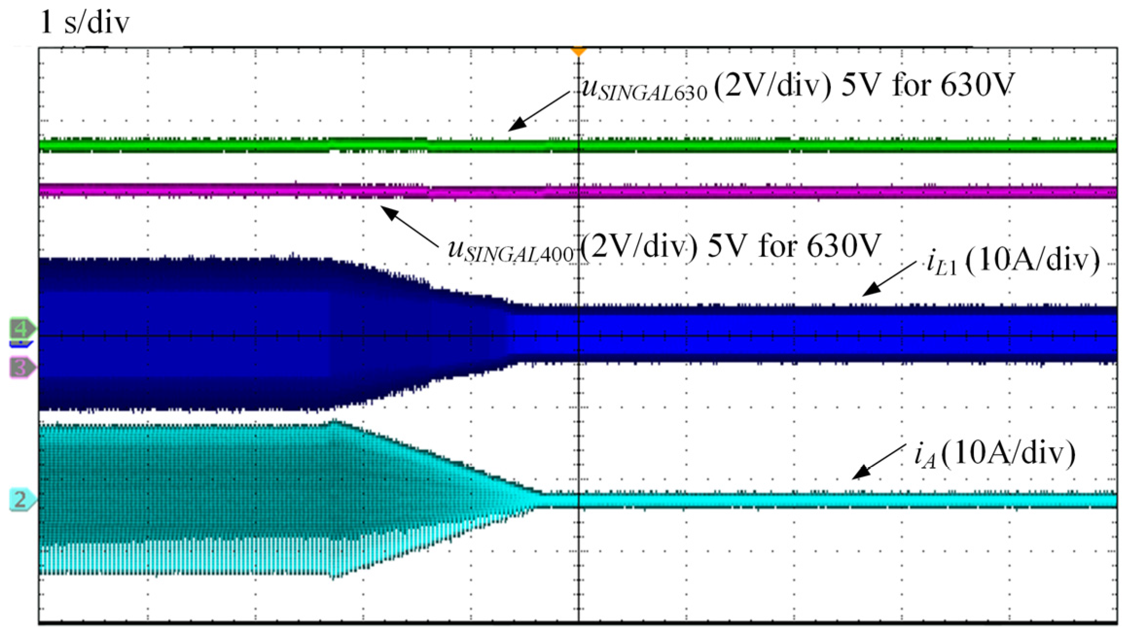
6.3. Experimental Results with Real Household Load

In order to verify the availability of the improved control method for the residential PV system, experiments are conducted with real household loads. Here the 400 V DC bus voltage and the 630 V DC bus voltage are observed through a real time sampling device, uSIGNAL400 represents 400 V DC bus voltage, and uSIGNAL630 represents 630 V DC bus voltage.

6.3.1. Experimental Results with Air Conditioner in On-Line Mode

A 4-kW air conditioner is used as an AC load in on-line mode. Figure 23 shows the transient waveforms when the air conditioner is shutdown. During this transition, the currents of LLC and inverter decline slowly, and the LLC converter always works in full-bridge mode. The 400 V and 630 V DC bus voltage are flat and the entire system is stable. Here iL1 is current of first channel LLC resonant inductor, and iA is inverter output current of phase A.

6.3.2. Experimental Results with Microwave and Refrigerator in Off-Line Mode

In order to verify the impact loading response ability of the proposed control method, a 1.5 kW microwave oven and a 200 W refrigerator are used. Figure 24 shows the waveforms during turning-on operations of the two loads. The 630 V DC bus voltage, phase voltage of inverter and first channel LLC working frequency, are observed through the same real time sampling device. Here uSIGNALA represents phase A voltage, fSIGNALs1 represents working frequency of first channel LLC. During this period, LLC transforms from half-bridge to full-bridge mode as its working frequency shows, u630 declines to 555 V and recovers after 30 ms, the steady fluctuation is about 60 V. The distorted current is caused by the microwave and refrigerator, which don’t have power factor correction ability. The entire system is stable.

7. Conclusions

In this work, a new method to regulate voltage for a full-bridge LLC resonant converter under light load conditions is proposed to solve the voltage gain curve upwarp drift problem. This method transforms a full-bridge LLC resonant converter into a half-bridge LLC resonant converter by adapting PFM driver signals simply. Ideal and actual FHA models are analyzed based on previous reference method. Furthermore, a new voltage and current sharing control scheme in on-line and off-line mode to enhance LLC performance in a residential PV system is implemented. Based on this control scheme, the DC bus voltage is regulated smoothly in all load range, and the two LLC resonant inductor currents are shared well.
Matlab simulation and experimental results, based on resistive load, are performed in the laboratory. In on-line mode, steady-state error of 400 V DC bus voltage is eliminated under light load conditions. During load transition from 0 to 7 kW, the 400 V DC bus voltage has a drop of 14 V in simulation and stays stable in the experiments. The settling time declines from 0.35 s to almost 0 in the experiments. CUF is almost 0 in the simulation and 1.7% in the experiments. In off-line mode, burst mode is eliminated and ripple is restrained. During load transition from 0 to 7 kW, 630 V DC bus voltage has a drop of 42 V and a rise of 11 V in simulation, while it has a drop of 41 V and a rise of 12 V in the experiments. The settling time declines from 0.63 s to 21 ms in the experiments. CUF is almost 0 in simulation and 0.7% in the experiments. Furthermore, the experimental results have also been carried out with real household loads. The waveforms show that the improved residential PV system can work stably with real household loads such as an air conditioner, microwave oven and refrigerator.

Acknowledgments

This research was supported by the National High Technology Research and Development Program (863 Program) of China (Grant: 2015AA050603). The authors would also like to thank the anonymous reviewers for their valuable comments and suggestions to improve the quality of the paper.

Author Contributions

Shu-Huai Zhang, Feng-Zhang Luo and Yi-Feng Wang proposed the control method, completed theoretical analysis and simulation. Feng-Zhang Luo is also responsible for writing and revising the paper. Jiang-Hua Liu, Yong-Peng He and Yue Dong helped in modifying control algorithm and conducting experiments.

Conflicts of Interest

The authors declare no conflict of interest.

References

  1. Kim, Y. Modeling and Analysis of a DC Electrical System and Controllers for Implementation of a Grid-Interactive Building. Energies 2017, 10, 427. [Google Scholar] [CrossRef]
  2. Jung, S.; Kim, D. Pareto-Efficient Capacity Planning for Residential Photovoltaic Generation and Energy Storage with Demand-Side Load Management. Energies 2017, 10, 426. [Google Scholar] [CrossRef]
  3. Wang, Y.; Lin, X.; Pedram, M. Adaptive Control for Energy Storage Systems in Households with Photovoltaic Modules. IEEE Trans. Smart Grid 2014, 5, 992–1001. [Google Scholar] [CrossRef]
  4. Ahmed, T.; Soon, T.; Mekhilef, S. A Single Phase Doubly Grounded Semi-Z-Source Inverter for Photovoltaic (PV) Systems with Maximum Power Point Tracking (MPPT). Energies 2014, 7, 3618–3641. [Google Scholar] [CrossRef]
  5. Chen, W.; Yang, X.; Zhang, W.; Song, X. Leakage Current Calculation for PV Inverter System Based on a Parasitic Capacitor Model. IEEE Trans. Power Electron. 2016, 31, 8205–8217. [Google Scholar] [CrossRef]
  6. Tsai, C.; Shen, C.; Su, J. A Power Supply System with ZVS and Current-Doubler Features for Hybrid Renewable Energy Conversion. Energies 2013, 6, 4859–4878. [Google Scholar] [CrossRef]
  7. Isoda, H.; Kimura, G.; Shioya, M.; Ohsato, M.H. Battery charging characteristics in small scaled photovoltaic system using resonant DC-DC converter with electric isolation. In Proceedings of the International Conference on Industrial Electronics, Control, and Instrumentation (IECON), Pacific Grove, CA, USA, 23–27 November 1990; Volume 2, pp. 1118–1123. [Google Scholar]
  8. Zhan, W.; Li, H. An Integrated Three-Port Bidirectional DC–DC Converter for PV Application on a DC Distribution System. IEEE Trans. Power Electron. 2013, 28, 4612–4624. [Google Scholar]
  9. Yang, B.; Lee, F.C.; Zhang, A.J.; Huang, G. LLC resonant converter for front end DC/DC conversion. In Proceedings of the Applied Power Electronics Conference and Exposition, Dallas, TX, USA, 10–14 March 2002; Volume 2, pp. 1108–1112. [Google Scholar]
  10. Jin, K.; Ruan, X. Hybrid full-bridge three-level LLC resonant converter—A novel dc-dc converter suitable for fuel cell power system. IEEE Trans. Ind. Electron. 2006, 53, 1492–1503. [Google Scholar] [CrossRef]
  11. Yang, B.; Chen, R.; Lee, F.C. Integrated magnetic for LLC resonant converter. In Proceedings of the Applied Power Electronics Conference and Exposition, Dallas, TX, USA, 10–14 March 2002; Volume 1, pp. 346–351. [Google Scholar]
  12. Jung, J.; Kim, H.; Ryu, M.; Baek, J. Design methodology of bidirectional CLLC resonant converter for high-frequency isolation of DC distribution systems. IEEE Trans. Power Electron. 2013, 28, 1741–1755. [Google Scholar] [CrossRef]
  13. Jiang, T.; Zhang, J.; Wu, X.; Sheng, K.; Wang, Y. A Bidirectional LLC Resonant Converter with Automatic Forward and Backward Mode Transition. IEEE Trans. Power Electron. 2015, 30, 757–770. [Google Scholar] [CrossRef]
  14. Zhang, J.; Liao, J.; Wang, J.; Qian, Z. A current-driving synchronous rectifier for an LLC resonant converter with voltage-doubler rectifier structure. IEEE Trans. Power Electron. 2012, 27, 1894–1904. [Google Scholar] [CrossRef]
  15. Han, J.H.; Lim, Y.C. Design of an LLC Resonant Converter for Driving Multiple LED Lights Using Current Balancing of Capacitor and Transformer. Energies 2015, 8, 2125–2144. [Google Scholar] [CrossRef]
  16. Jiang, J.; Pidaparthy, S.K.; Choi, B. Current Mode Control for LLC Series Resonant DC-to-DC Converters. Energies 2015, 8, 6098–6113. [Google Scholar] [CrossRef]
  17. Cho, S.; Kim, C.; Han, S. High-efficiency and low-cost tightly regulated dual-output LLC resonant converter. IEEE Trans. Ind. Electron. 2012, 59, 2982–2991. [Google Scholar] [CrossRef]
  18. Hyeon, B.C.; Cho, B.H. Analysis and Design of the LLC Resonant Converter for Low Output Current Ripple. IEEE Trans. Ind. Electron. 2012, 59, 2772–2780. [Google Scholar] [CrossRef]
  19. Fang, X.; Hu, H.; Shen, Z.J.; Batarseh, I. Operation mode analysis and peak gain approximation of the LLC resonant converter. IEEE Trans. Power Electron. 2012, 27, 1985–1995. [Google Scholar] [CrossRef]
  20. Yang, B. Topology Investigation of Front-End DC/DC Converter for Distributed Power System. Ph.D. Thesis, Virginia Tech, Blacksburg, VA, USA, September 2003. [Google Scholar]
  21. Kim, J.H.; Kim, C.E.; Kim, J.K.; Moon, G.W. Analysis for LLC resonant converter considering parasitic components at very light load condition. In Proceedings of the 8th International Conference on Power Electronics, Jeju, Korea, 30 May–3 June 2011; pp. 1863–1868. [Google Scholar]
  22. Lee, B.H.; Kim, M.Y.; Kim, C.E.; Park, K.-B.; Moon, G.W. Analysis of LLC resonant converter considering effects of parasitic components. In Proceedings of the INTELEC 31st International Telecommunications Energy Conference, Incheon, Korea, 18–22 October 2009; pp. 1–6. [Google Scholar]
  23. Pan, H.; He, C.; Ajmal, F.; Chen, H.; Chen, G. Pulse-width modulation control strategy for high efficiency LLC resonant converter with light load applications. IET Power Electron. 2014, 7, 2887–2894. [Google Scholar] [CrossRef]
  24. Hu, Z.; Liu, Y.F.; Sen, P.C. Bang-Bang charge control for LLC resonant converters. IEEE Trans. Power Electron. 2015, 30, 1093–1108. [Google Scholar]
  25. Kowstubha, P.; Krishnaveni, K.; Reddy, K.R. Review on different control strategies of LLC series resonant converters. In Proceedings of the 2014 International Conference on Advances in Electrical Engineering (ICAEE), Vellore, India, 9–11 January 2014; pp. 1–4. [Google Scholar]
  26. Pahlevaninezhad, M.; Eren, S.; Jain, P.; Bakhshai, A. Self-sustained oscillating control technique for current-driven full-bridge DC/DC converter. IEEE Trans. Power Electron. 2013, 28, 5293–5310. [Google Scholar] [CrossRef]
  27. Kim, B.C.; Park, K.B.; Moon, G.W. Asymmetric PWM control scheme during hold-up time for LLC resonant converter. IEEE Trans. Ind. Electron. 2012, 59, 2992–2997. [Google Scholar] [CrossRef]
  28. Musavi, F.; Cracium, M.; Gautam, D.S.; Eberle, W. Control strategies for wide output voltage range LLC resonant DC–DC converters in battery chargers. IEEE Trans. Veh. Technol. 2014, 63, 1117–1125. [Google Scholar] [CrossRef]
  29. Feng, W.; Lee, F.C.; Mattavelli, P. Optimal trajectory control of burst mode for LLC resonant converter. IEEE Trans. Power Electron. 2013, 28, 457–466. [Google Scholar] [CrossRef]
  30. Jung, J.H.; Kwon, J.G. Theoretical analysis and optimal design of LLC resonant converter. In Proceedings of the European Conference on Power Electronics and Applications, Aalborg, Denmark, 2–5 September 2007; Volume 1, pp. 1–10. [Google Scholar]
  31. Simone, S.D.; Adragna, C.; Spini, C.; Gattavari, G. Design-oriented steady-state analysis of LLC resonant converters based on FHA. In Proceedings of the International Symposium on Power Electronics, Electrical Drives, Automation and Motion IEEE, Taormina, Italy, 23–26 May 2006; pp. 200–207. [Google Scholar]
Figure 1. Architecture of residential photovoltaic system.
Energies 10 00752 g001
Figure 2. Ideal equivalent circuit of LLC resonant converter
Energies 10 00752 g002
Figure 3. Equivalent model of LLC resonant converter considering parasitic parameters.
Energies 10 00752 g003
Figure 4. Voltage gain curve of full-bridge LLC converter at light load condition.
Energies 10 00752 g004
Figure 5. Drive signals of the proposed changing topological LLC: (a) Full-bridge LLC; and (b) Half-bridge LLC.
Energies 10 00752 g005
Figure 6. Voltage gain curve of half-bridge LLC.
Energies 10 00752 g006
Figure 7. Design procedure of the proposed full-bridge LLC converter.
Energies 10 00752 g007
Figure 8. Voltage gain and frequency range selection in full-bridge and half-bridge LLC.
Energies 10 00752 g008
Figure 9. Hysteresis controller for the transform signal generation.
Energies 10 00752 g009
Figure 10. LLC control scheme in on-line mode.
Energies 10 00752 g010
Figure 11. Simulation results in on-line mode: (a) transition waveforms; and (b) steady state waveforms with light load.
Energies 10 00752 g011
Figure 12. Two channel LLC currents in on-line mode during load transition from 0 to 7 kW load.
Energies 10 00752 g012
Figure 13. LLC control scheme in off-line mode.
Energies 10 00752 g013
Figure 14. Simulation results in off-line mode: (a) transition waveforms; and (b) steady state waveforms with light load.
Energies 10 00752 g014
Figure 15. Two channel LLC currents in off-line mode during load transition from 0 to 7 kW.
Energies 10 00752 g015
Figure 16. 7 kW residential photovoltaic system hardware setup.
Energies 10 00752 g016
Figure 17. Waveforms of AC load increases from 0 to 7 kW in on-line mode with the original control method.
Energies 10 00752 g017
Figure 18. Waveforms of AC load increases from 0 to 7 kW in on-line mode with the original control method.
Energies 10 00752 g018
Figure 19. Waveforms of AC load transition from 7 kW to 0 in on-line mode with the new control scheme.
Energies 10 00752 g019
Figure 20. Waveforms of AC load increases from 0 to 7 kW in off-line mode with the original control method.
Energies 10 00752 g020
Figure 21. Waveforms of AC load transition from 0 to 7 kW in off-line mode.
Energies 10 00752 g021
Figure 22. Waveforms of AC load transition from 7 kW to 2.3 kW to 0 in off-line mode.
Energies 10 00752 g022
Figure 23. Waveforms when 4 kW air conditioner shutdown in on-line mode.
Energies 10 00752 g023
Figure 24. Waveforms when turn on microwave oven and refrigerator in off-line mode.
Energies 10 00752 g024
Table 1. Simulation Parameters.
ParameterValue
LLC main resonant frequency, fr78.8 kHz
LLC secondary resonant frequency, fr236.0 kHz
First channel LLC resonant inductor, Lr160 μH
First channel LLC resonant capacitor, Cr168 nF
First channel LLC Magnetizing inductor, Lm1228 μH
Second channel LLC resonant inductor, Lr265 μH
Second channel LLC resonant capacitor, Cr268 nF
Second channel LLC Magnetizing inductor, Lm2223 μH
400 V DC bus capacitor200 μF
630 V DC bus capacitor200 μF
AC bus voltage380 V (phase to phase)
Table 2. Experimental parameters.
ParameterValue
LLC rated power4 kW (one channel)
LLC main resonant frequency, fr178.8 kHz
LLC secondary resonant frequency, fr236.0 kHz
LLC resonant inductor, Lr60 μH
LLC resonant capacitor, Cr68 nF
LLC Magnetizing inductor, Lm228 μH
LLC MOSFET (primary side)IPW65R045C7 (Infineon, Munich, Germany)
LLC diode rectifier (secondary side)C4D10120E (Cree, Durhmorning, America)
Battery voltage100 V DC
PV maximum power3.5 kW
400 V DC bus capacitor200 μF
630 V DC bus capacitor200 μF
AC bus voltage380 V (phase to phase)
coefficient k112.5 Hz/V
coefficient k262.5 Hz/V
Step3, Δf3500 Hz

