Article

An Input-Parallel-Output-Series Switched-Capacitor Three-level Boost Converter with a Three-Loop Control Strategy

1
State Key Laboratory of Power Transmission Equipment & System Security and New Technology, Chongqing University, Chongqing 400044, China
2
Department of Electrical and Computer Engineering, Wayne State University, Detroit, MI 48202, USA
*
Author to whom correspondence should be addressed.
Energies 2018, 11(10), 2631; https://doi.org/10.3390/en11102631
Submission received: 2 September 2018 / Revised: 22 September 2018 / Accepted: 28 September 2018 / Published: 2 October 2018

Abstract

:
There has been increasing interest for industry applications, such as solar power generation, fuel cell systems, and dc microgrids, in step-up dc-dc converters with reduced number of components, low component stress, small input ripples and high step-up ratios. In this paper, an input-parallel-output-series three-level boost (IPOS-SC-TLB) converter is proposed. In addition to achieving the required performance, the input and output terminals can share the same ground and an automatic current balance function is also achieved in the IPOS-SC-TLB converter. Besides, a capacitor voltage imbalance mechanism was revealed and a three-loop control strategy composed of output voltage loop, input current loop and voltage-balance loop was proposed to address the voltage imbalance issue. Finally both simulation and experiment studies have been conducted to verify the effectiveness of the IPOS-SC-TLB converter and the three-loop control strategy.

1. Introduction

Multilevel step-up dc-dc converters are widely employed in wind farms [1,2,3,4,5,6], solar power generation systems [7,8,9,10,11], fuel cell systems [12,13,14,15], high-power charging stations for electric cars [16,17], and dc microgrids [18,19,20]. In these systems, a multilevel step-up dc-dc converter helps regulate a varying low-level input voltage to a stable high-level voltage, which usually serves as the dc link voltage of a grid-connected inverter. It is desirable to achieve both low voltage stress and low current stress across components to reduce power losses and save cost. Besides, input current ripple is another important issue that should be considered for these systems, especially for fuel cell or battery storage systems. As multilevel conversion techniques have evolved, many multilevel step-up dc-dc converters have been proposed. In terms of non-isolated multilevel step-up dc-dc converters, the three-level boost converter was firstly proposed and then adopted to combine with a three-level diode-clamped inverter to achieve medium voltage and high power [2,6]. The corresponding four-level boost converter was subsequently proposed to output higher voltage level and higher power [4]. Owing to the interleaved scheme, small input current ripple and low component stress could be easily realized in these multilevel boost converters. However, the input terminal and the output terminal in the two converters do not share the same ground, which can bring in severe EMI problem [7]. One flying-capacitor-based three-level boost converter was proposed to address this problem and good effect has been achieved [12]. However, all these multilevel boost converters face the same inherent limitation, i.e., the voltage gain is limited to be 1/(1 − d), where d is the duty ratio. Unfortunately, practical considerations limit its output voltage to approximately four times its input voltage. To supply a high output voltage, it must operate at extremely high duty-cycle whereas extreme duty-cycles impose inefficient small off times. Small off times will cause severe diode reverse-recovery currents, increasing electromagnetic interference (EMI) levels [9].
Another flying-capacitor-based three-level boost converter with intrinsic voltage doubler was proposed in [21,22]. In addition to the advantages of topology described in [8], the two input inductor currents of this converter could be self-balanced due to the flying-capacitor. Moreover, the voltage gain of this converter is 2/(1 − d) instead of 1/(1 − d). However, the voltage stresses across the output diode and the output capacitor equals to the output voltage, which is a disadvantage. On the other hand, the voltage stresses across the output diodes could be decreased by half of the output voltage in the converter with two symmetrical flying-capacitors [23]. Nevertheless, one more diode and one more capacitor are necessary, and voltage stress across the output capacitor is still very high. These shortcomings are also presented in the topologies proposed in [24,25]. In general, a list of split capacitors connected in series is a good solution to reducing voltage stress across the output capacitor. One solution is the application of a diode-capacitor voltage multiplier on a classical non-isolated boost converter, which also presents a high voltage gain and self-balanced function for capacitor voltages [26]. However, a large input current ripple and a high current stress across the single switch exist inevitably as no interleaved scheme is adopted in these converters. Modular multilevel dc-dc converter is a good choice for high voltage applications, such as high voltage direct current (HVDC) and high voltage drive areas [27,28,29,30,31]. However, it is not a good choice for medium-voltage applications. Reference [32] proposed a modular multilevel dc-dc converter composed of multiple buck-boost converter modules, which is suitable for medium-voltage and high-power applications. However, the output voltage of the lower module multiplying by d/(1 − d) serves as the input voltage of the upper module, to achieve a high voltage gain. The voltage gain is smaller than 2/(1 − d) and all switches do not share the same ground. Recently, a switched-capacitor technique has begun to be employed in medium-voltage and high-power dc-dc converters with good performance [33,34,35,36].
To address the abovementioned issues and to achieve a reduced number of components, low component stress, small input ripples and high step-up ratio, an input-parallel-output-series switched-capacitor three-level boost (IPOS-SC-TLB) converter is proposed in this paper. In addition to achieving the required performance target, the proposed IPOS-SC-TLB converter also has automatic current balancing capability. Compared with the existing three-level boost converters, the proposed converter has the advantages of high voltage gain at full duty cycle range, small component stress, a reduced number of components, common ground for the input and output terminals, and automatic current balancing. All capacitors, diodes, switches only endure half of the output voltage, enabling components with less voltage rating used in the proposed IPOS-SC-TLB converter. Common ground for the input and output terminals not only save power supplies for designing drivers, also helps reduce EMI. Automatic current balancing capability avoid additional current-balance control strategy that is required in a multi-converter system. To address the voltage imbalance issue, a three-loop control strategy composed of an output voltage loop, an input current loop and a voltage-balance loop is developed for the IPOS-SC-TLB converter.
The remainder of the paper is organized as follows: Section 2 introduces the topology derivation and operating principle of the proposed IPOS-SC-TLB converter. Performance analysis is subsequently presented in Section 3 and the three-loop control strategy is given in Section 4. Both simulation and experimental verifications have been done in Section 5 and finally the conclusions of the paper are drawn in Section 6.

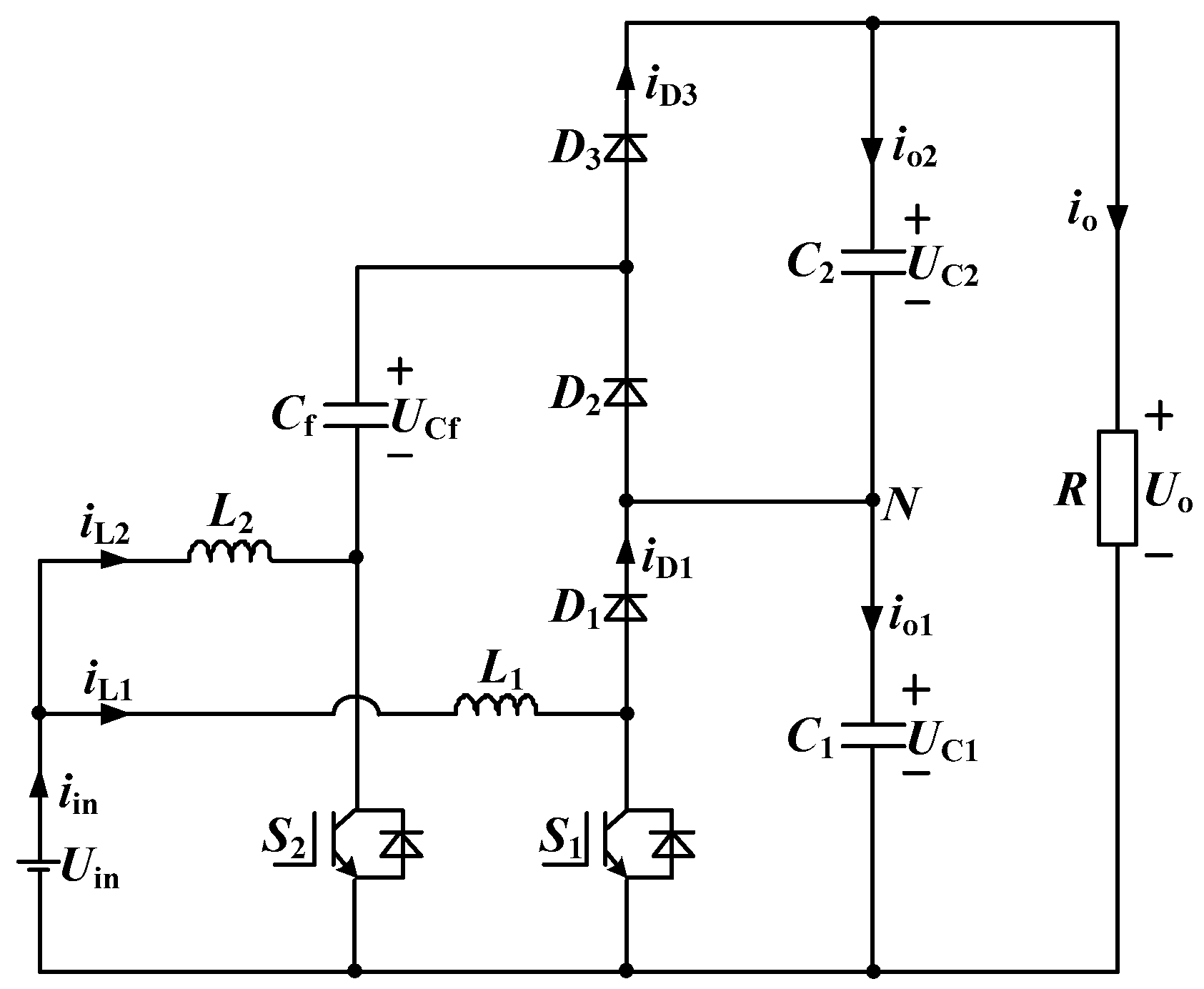
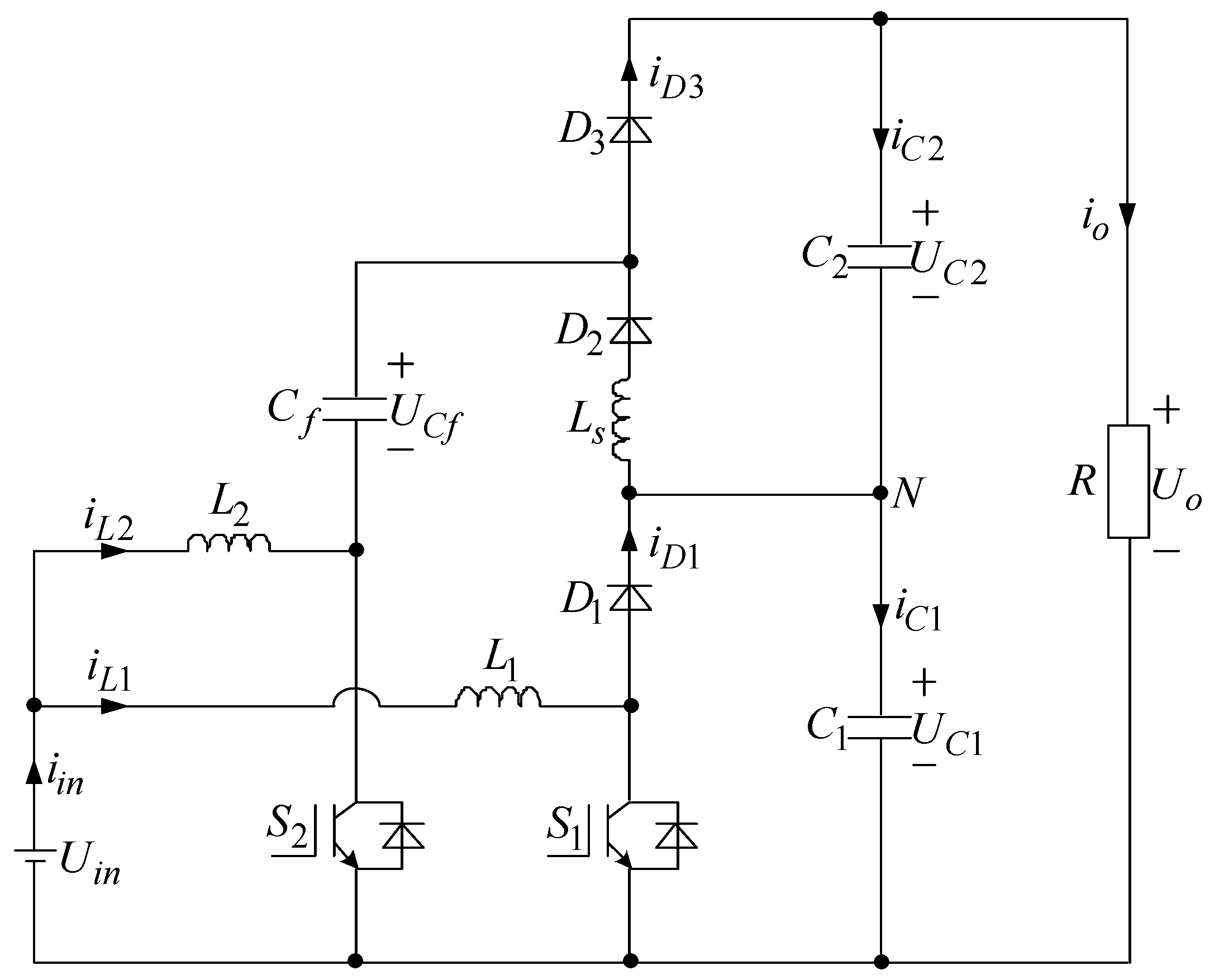
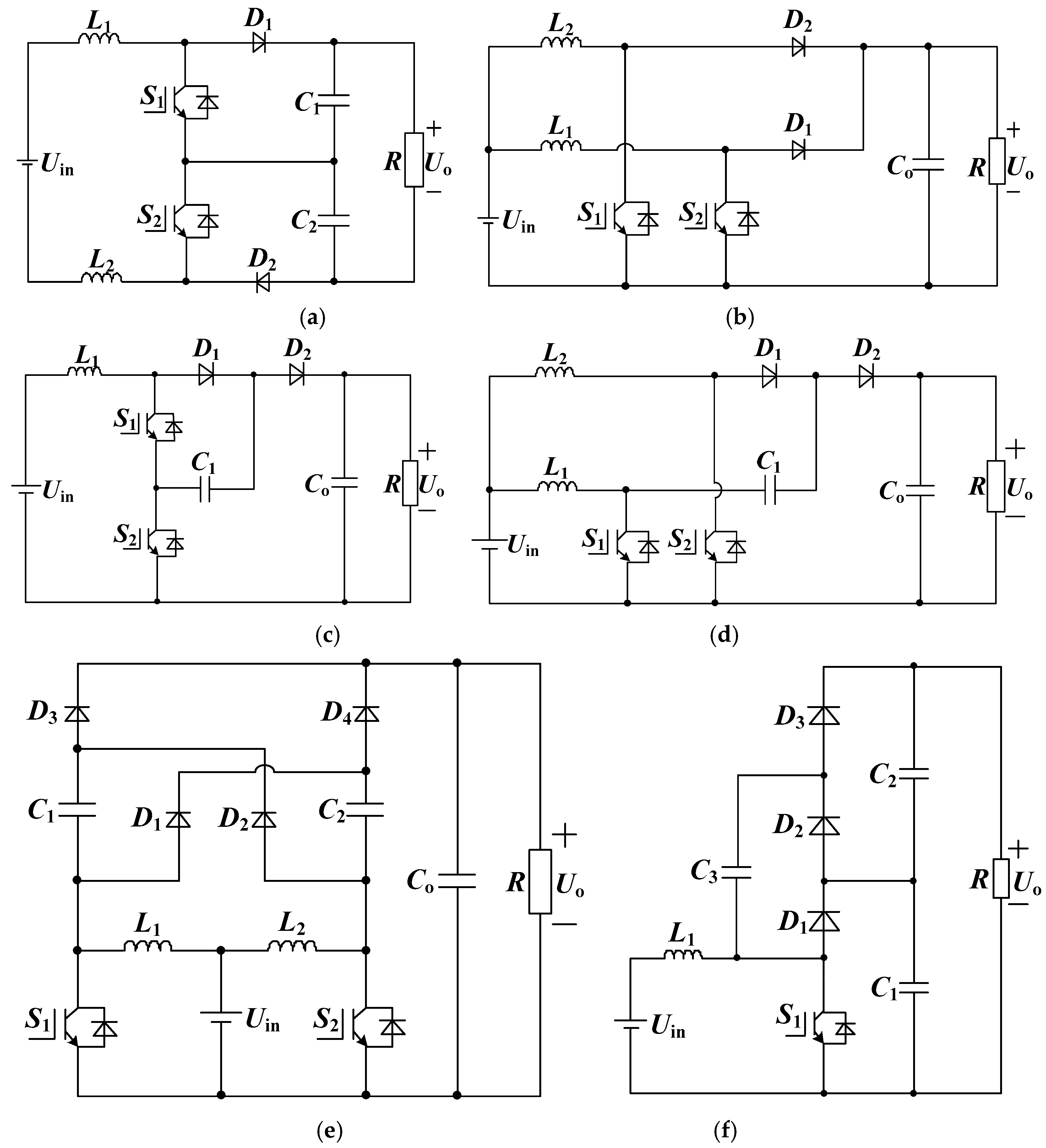
2. IPOS-SC-TLB Converter

2.1. Topology Derivation

Until now, interleaved techniques adopted in multilevel dc-dc converters can be divided into two different types: serial-interleaved (SI) techniques (Figure 1a) and parallel-interleaved (PI) techniques (Figure 1b). As it can be seen, the total components of the two topologies are equal except the numbers of inductors and capacitors. One inductor is necessary in the SI structure while (n − 1) inductors are employed in the PI structure. The SI structure needs (n − 1) capacitors, while one capacitor is necessary in the PI structure.
A comparative analysis between the two techniques are presented in Table 1. On the one hand, (n − 1) voltage levels U0, U1, … Un−1, are achieved due to the (n − 1) split capacitors in the SI structure while only one output voltage level Un−1 is achieved in the PI structure. On the other hand, the total input current flow through (n − 1) split inductors in the PI structure while through only one inductor in the SI structure. As a result, the SI structure has output voltage divider function and voltage-balance control strategy is necessary to realize voltage balance. The PI structure has input current shunt function and current-balance control strategy is necessary to balance all split inductor currents. All the drive circuits of the switches must be isolated in the SI topology, i.e., (n − 1) isolated drive sources are necessary in the SI structure. However, this drawback does not exist in the PI structure because all the switches share the same ground.
The conventional three-level boost converter is based on the SI structure in Figure 2a. To distinguish it from other topologies in this paper, the converter in Figure 2a is called SI-TLB. The converter in Figure 2b is named as PIB as it is based on the PI topology. The input terminal and the output terminal of SI-TLB do not share the same ground, which easily results in electromagnetic interference (EMI) problems. Moreover, the voltage stresses across all the components in a PIB converter are high since no multilevel technique is employed.
To avoid these shortcomings mentioned above, flying-capacitor technique has been introduced into SI-TLB and PIB converters to develop new three-level boost converters. The converter called SI-FC-TLB in Figure 2c is derived by employing one flying-capacitor. The input terminal and the output terminal share the same ground and all switches and diodes are clamped at the half of the output voltage by controlling the voltage of the flying-capacitor Cf to be half of the output voltage [21,22]. However, it can be seen that SI-TLB and SI-FC-TLB both have a limited voltage gain due to the SI structure. Thus, the converter called PI-FC-TLB in Figure 2d was proposed based on PI structure and one flying-capacitor [21,22]. The voltage gain of PI-FC-TLB is as two times as that of SI-TLB and SI-FC-TLB. But the voltage stress across the output diode is high, equal to the output voltage. Also, another converter PI-SFC-TLB based on the PI structure and two symmetrical flying-capacitors in Figure 2e was proposed to reduce the voltage stresses across the output diodes [23]. However, the voltage stress across the output capacitor is still equal to the output voltage and many capacitors and diodes are necessary. As analyzed above, flying-capacitor technique introduced into multilevel boost converters based on SI structure could help solve the problem that input and output terminals do not share the same ground while flying-capacitor technique introduced into multilevel boost converters based on PI structure could help enhance voltage gains. However, there is a common disadvantage among SI-FC-TLB, PI-FC-TLB, and PI-SFC-TLB converters that the output terminal is constructed by only one output capacitor, which not only bears a high voltage stress, but also does not help reduce the voltage stress across output diodes and output capacitors. Additionally, the voltage-balance control is not easy to realize as one or more flying-capacitor voltages should be control independently. Even though the output capacitor can be replaced by two split capacitors in series in the output terminal, the two split capacitors could not be self-balanced and could not be controlled by voltage-balance control strategy either. On the other hand, a three-level boost converter based on switched-capacitor network is proposed in [26]. For simplification, the converter is name as SC-TLB, which not only has two split capacitors at the output terminal, but also has self-balancing function for capacitor voltages. As a result, there is no need to employ any voltage-balance control strategies to solve the voltage imbalance issue. However, as analyzed in Section 1, there is a big disadvantage that SC-TLB has high input current and high input current ripple since no interleaved structures are employed. As a result, high power losses are inevitable in the SC-TLB converter.
There are also two input-parallel-output-series (IPOS) boost converters shown in Figure 2g (called by IPOS-TLB1) and Figure 2h (called by IPOS-TLB2) from references [24,25]. Like the ISOS-TLB converter, the input terminal and the output terminal do not share the same ground and the voltage stress across diode D1 is equal to the output voltage in the IPOS-TLB1 converter. Although the topology IPOS-TLB2 is simple, its voltage gain is smaller than the other topologies and the input terminal and the output terminal do not share the same ground, either.
According to the comparative analysis mentioned above, the SI structure is suitable for high input voltage and high output voltage applications while the PI structure is suitable for high input current and high output current applications. As shown in Figure 1, the input terminal, output terminal and all switches share the same ground in the PI topology. The flying-capacitor technique helps enhance the voltage gains of the converters based on the PI structure. Besides, the switched-capacitor technique, which could be deemed as an extension of flying-capacitor technique, not only increases the voltage gain, but also brings a self-balancing function for capacitor voltages. On the whole, there are three techniques could be employed in multilevel dc/dc converters, i.e., interleaved technique, flying-capacitor technique, and switched-capacitor technique. Until now, only one or two of the three techniques were employed in a single power converter.
This paper proposes an IPOS-SC-TLB converter in Figure 3 and presents a detailed analysis of the converter. IPOS-SC-TLB combines the parallel-interleaved technique, flying-capacitor technique, and switched-capacitor technique together. In Figure 3, L1, L2, S1, S2 formulate the PI structure, while L1, S1, D1, C1 form Boost I and L2, S2, D3, C2 form Boost II. Besides, Cf, D2 and S2, C1 formulate a switched-capacitor network, which makes the two input terminals in parallel and the output terminals in series for Boost I and Boost II.

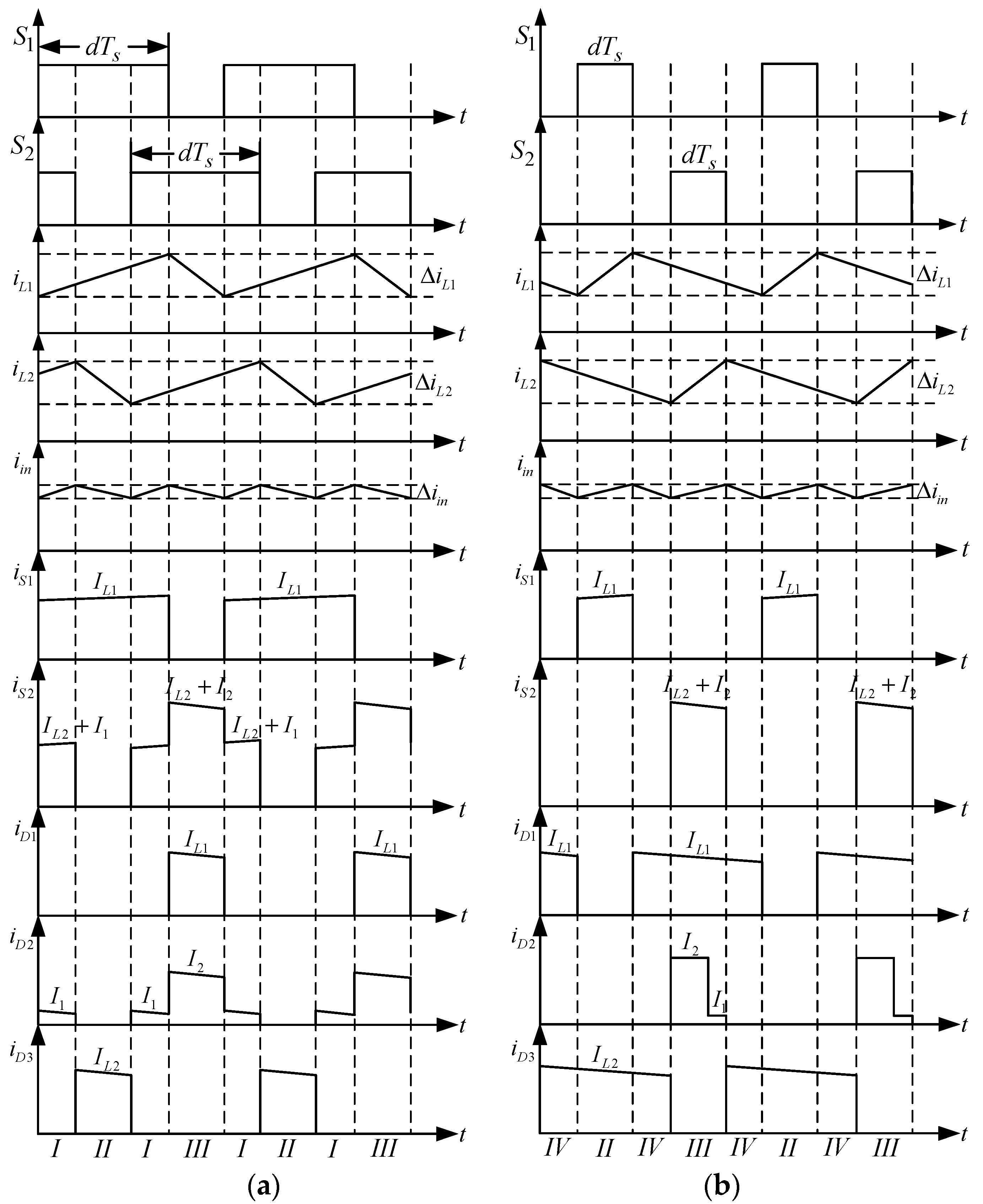
2.2. Operating Principle

In the IPOS-SC-TLB converter, all the inductors, capacitors, switches, diodes have the same respective parameters, i.e.,
L 1 = L 2 = L  
C 1 = C 2 = C  
Considering the voltage drops of IGBT and diode, and the equivalent series resistor of inductor, the equivalent circuits of the IPOS-SC-TLB converter are presented in Figure 4. In the interleaved scheme, the operating stages of IPOS-SC-TLB could be divided into two modes according to duty cycle: when d is greater than 0.5 and when d is smaller than 0.5.
(1) When the duty cycle d is greater than 0.5, the IPOS-SC-TLB operates at the periodic stages of I, II, I, and III.
Stage I: Both switches S1, S2 are turned on and the diode D2 is forward biased as the capacitor voltage UC1 is still a little bigger than the capacitor voltage UCf after the stage III. During Stage I, both the two inductors L1, L2 are charged by the input source Uin. Thus, there are:
L 1 d i L 1 d t = L 2 d i L 2 d t = U i n I L 1 r L U S  
U C 1 = U C f + U S + U D  
As the two capacitor voltages UC1, UCf are charged in parallel, the voltage differences between UC1 and UCf are small but cannot be ignored. As a result, the current flowing through D2 caused by the small voltage difference is labelled as I1. The current flowing through S1 is equal to iL1 while the current flowing through S2 is the sum of iL2 and I1.
Stage II: When the switch S1 is turned on and the switch S2 is turned off, the diode D3 is forward. The inductor L1 is still charged by the input source Uin, which also supplies energy to the load together with the inductor L2 and the flying-capacitor Cf. Thus, there are:
L 1 d i L 1 d t = U i n I L 1 r L U S  
L 2 d i L 2 d t = U i n + U C f U D U C 2 U C 1  
According to (4) and (6), there is:
L 2 d i L 2 d t = U i n U C 2 U S 2 U D  
During Stage II, the capacitor voltage UCf decreases while the capacitor voltage UC1 increases. As a result, the voltage difference between UC1 and UCf becomes bigger and bigger and finally reaches its maximum at the end of Stage II. The current flowing through the switch S1 is still equal to iL1 while no currents flows through the switch S2 and the diode D2 during this stage.
Stage I: The converter repeats Stage I and the same output results could be achieved like (3) and (4). However, as analyzed in Stage II, the voltage difference between UC1 and UCf reaches its maximum value, the current flowing through the diode D2 reaches its maximum value, labelled as I2. The current flowing through S1 turns to be the same as iL1 again while the current flowing through S2 is the sum of iL2 and I2.
Stage III: When the switch S1 is turned off while the switch S2 is turned on, the diodes D1, D2 are both forward. The inductor L2 is charged by the input source Uin, which also supplies energy to C1 and Cf together with the inductor L1. Thus, there are:
L 1 d i L 1 d t = U i n I L 1 r L U D U C 1  
L 2 d i L 2 d t = U i n I L 1 r L U S  
During Stage III, the two capacitors C1, Cf are connected in parallel and thus the voltage difference between them is small, which results in a small current flowing through the diode D2. It has been mentioned in the first Stage I, labelled as I1. As a consequence, the current flowing through S1 turns to be zero while the current flowing through S2 is the sum of iL2 and I1.
(2) When the duty cycle d is smaller than 0.5, the IPOS-SC-TLB converter operates at the periodic stages of IV, II, IV, and III.
Stage IV: Both switches S1, S2 are turned off while D1 and D3 are on forward biased:
L 1 d i L 1 d t = U i n I L 1 r L U D U C 1  
L 2 d i L 2 d t = U i n + U C f U D U C 2 U C 1 = U i n U C 2 U S 2 U D  
As the first Stage IV begins after Stage III, the capacitor voltage UCf decreases while the capacitor voltage UC1 increases. During this stage, no currents pass through the two switches S1, S2 and the diode D2 as they are all switched off.
Stage II: The same results could be achieved like (5)–(7) and the voltage difference between UC1 and UCf continues increasing during this stage. The current flowing through the switch S1 is still equal to iL1 while no currents flows through the switch S2 and the diode D2 during this stage.
Stage IV: The converter enters into another Stage IV, where the voltage difference between UC1 and UCf continues increasing and reach its maximum value at the end of the stage. And no currents no currents pass through the two switches S1, S2 and the diode D2.
Stage III: At the beginning of the stage III, the current flowing through the diode D2 reaches its maximum value I2. But later becomes a smaller value I1 as the two capacitors C1, Cf are charged in parallel. Thus, the current flowing through the switch S1 is zero while the current flowing through the switch S2 is the sum of iL2 and I2 and then the sum of iL2 and I1 during this stage. For any duty cycle d, two equations can be attained based on Voltage-Second Balance Principle during one switching period:
d T s ( U i n I L 1 r L U S ) + ( 1 d ) T s ( U i n I L 1 r L U D U C 1 ) = 0  
d T s ( U i n I L 2 r L U S ) + ( 1 d ) T s ( U i n U C 2 U S 2 U D ) = 0  
During the switching period, the output voltage of the converter is always described by:
U o = U C 1 + U C 2  
According to (28), there is:
I L 1 = I L 2 = U o R ( 1 d )  
Therefore, the voltage gain G and the capacitor voltages could be derived by:
G = U o U i n = 2 + ( 2 d 3 ) U D U S U i n 1 d + r L ( 1 + d ) R ( 1 d )  
The capacitor voltages are calculated by:
{ U C 1 = U i n I L 1 r L U D 1 d U C 2 = U i n d I L 2 r L U S + ( 2 d 2 ) U D 1 d U C f = U i n I L 1 r L ( 1 d ) U S ( 2 d ) U D 1 d  
When the parasitic parameters are ignored, there are:
{ G = 2 1 d U C 1 = U C 2 = U C f = 1 2 U o  

3. Performance Analysis

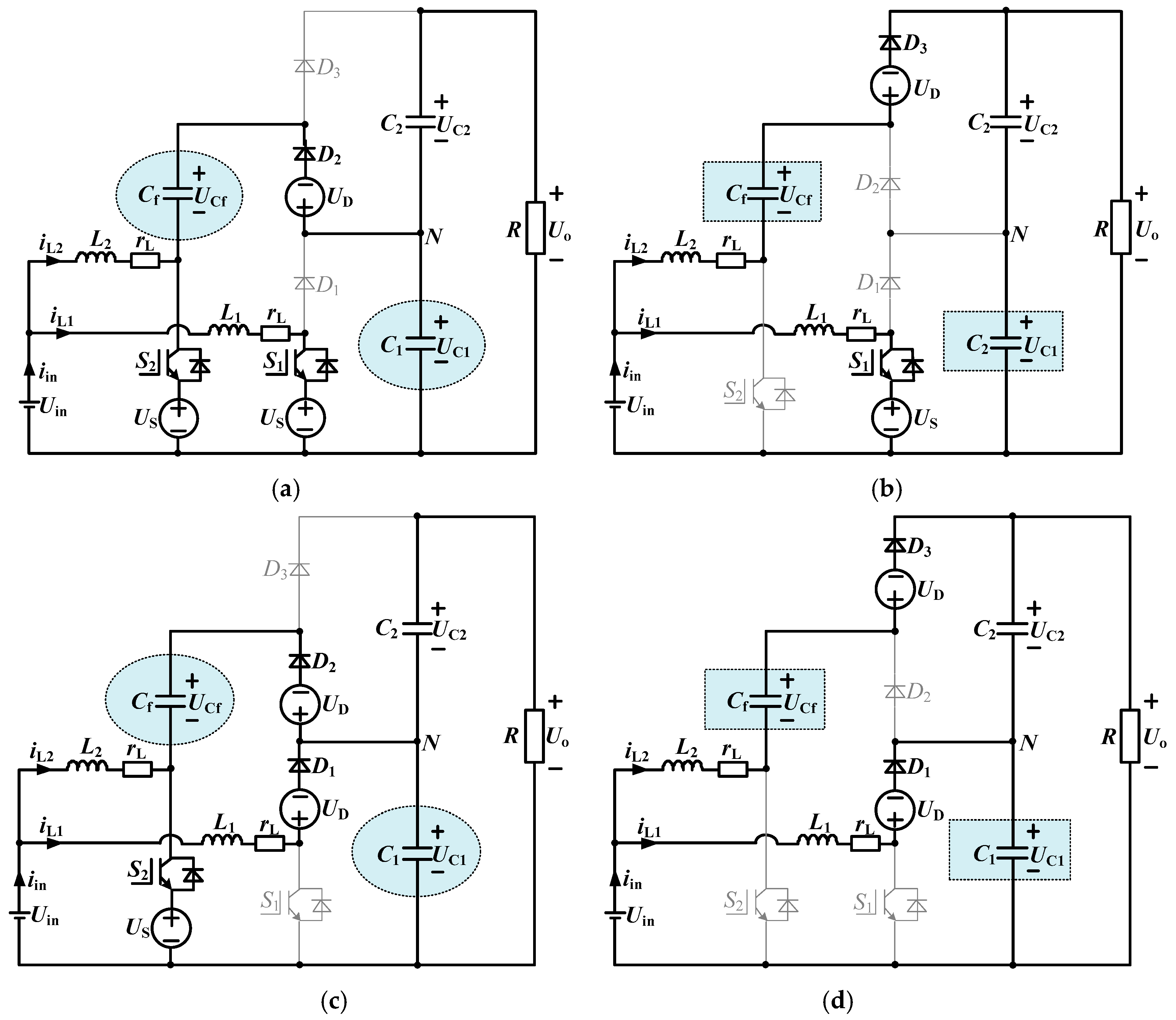
3.1. Component Stress

According to the analysis mentioned above, the key voltage waveforms of the IPOS-SC-TLB converter are presented in Figure 5. The voltage stresses across all switches, diodes and capacitors are half of the output voltage:
U S 1 = U S 2 = U D 1 = U D 2 = U D 3 = U C 1 = U C 2 = U C f = 1 2 U o  
The current waveforms of the IPOS-SC-TLB converter are presented in Figure 6. From Figure 6, whatever the duty cycle d is, the average current across S1, S2 can be obtained as follows:
{ I S 1 = d I L 1 I S 2 = I L 2  
The average currents across D1, D2, D3 identical with value equal to the average output current are determined as follows:
I D 1 = I D 2 = I D 3 = I o = U o R  
When the duty cycle d is over 0.5, the operating period of Stage II in Figure 4b can be expressed by (1 − d)Ts during one switching period. During Stage II, the capacitor C2 is charged with the current expressed by:
i C 2 _ charged = I L 2 U o R  
During the remained operating period dTs, C2 is discharged with the current expressed by:
i C 2 _ discharged = U o R  
According to Ampere-Second Balance Principle, there is:
( 1 d ) T s ( I L 2 U o R ) + d T s ( U o R ) = 0  
We can obtain the average current of inductor L2 by simplifying (24) as below:
I L 2 = U o R ( 1 d )  
When the duty cycle is smaller than 0.5, the same formula as (25) can be obtained. It should be noted that the average current of inductor L2 could be also derived as below. During one whole switching period, the average charging current flowing through Cf is the same as the average current flowing through D2. So the increased charges of Cf during one switching period is ID2*Ts. In addition, when d is over 0.5, the flying-capacitor Cf is only discharged during Stage II and the average discharging current flowing through Cf is IL2 with the discharging time (1 − d)Ts. When d is smaller than 0.5, the flying-capacitor Cf is discharged during Stage II and Stage IV with the average discharging current IL2 and the total discharged time (1 − d)Ts. It can be seen that the decreased charges of Cf during one switching period is IL2*(1 − d)Ts no matter what the duty cycle d is. Therefore, by applying Ampere-Second Balance Principle on Cf, we have:
I D 2 T s = I L 2 ( 1 d ) T s  
According to (26), the same formula as (25) can be achieved. On the other hand, the average current of L1 can be easily obtained as below:
I L 1 = I D 1 1 d = U o R ( 1 d )  
According to (20)–(27), the average currents across all switches and diodes are:
{ I L 1 = I L 2 = U o ( 1 d ) R I S 1 = d U o ( 1 d ) R I S 2 = U o ( 1 d ) R I D 1 = I D 2 = I D 3 = U o R  

3.2. Switched-Capacitor Network

For two typical boost converters, their input terminals cannot be simply connected in parallel and while their output terminals are connected in series simultaneously. The flying-capacitor Cf and the diode D2 in the proposed IPOS-SC-TLB converter are used to realize the input-parallel output-series topology. Because a switched-capacitor network is constructed and it helps support the output voltage of the Boost I for the Boost II. As shown in Figure 4, the flying-capacitor Cf is clamped with the capacitor C1 during Stage I and Stage III, labelled as the oval areas, i.e., the two capacitor voltages are identical. During Stage II and Stage IV, the flying-capacitor Cf serves as the voltage support for the Boost II. So, it could be thought of as that the output capacitor C2 is charged by the input source because the capacitor voltage UCf offsets the capacitor voltage UC1, which are labelled as the rectangular areas. Furthermore, it can be seen from (26) that the flying-capacitor Cf could automatically balance the average currents of the two inductors L1 and L2. Thus, the IPOS-SC-TLB converter does not need any current-balance circuit or current-balance control strategy that is required in the conventional parallel-interleaved dc/dc converters.

3.3. Ripple Analysis

In the switched-capacitor network, the flying-capacitor Cf could be served as an energy buffer. According to (26) and (27), the increased or decreased charges on Cf is Uo*Ts/R, which could be described by another way of CfuCf, where ΔuCf represents the voltage ripple of Cf. Finally, the voltage ripple of Cf is derived by:
Δ u C f = U o R C f f s  
Besides, it is easy to attain the voltage ripples of C1 and C2:
Δ u C 1 = Δ u C 2 = U o d R C f s  
Additionally, the current ripples of L1 and L2 could be obtained by:
Δ i L 1 = Δ i L 2 = U i n L d f s  
The input current ripple can be calculated by:
Δ i i n = { U i n L 2 d 1 f s d > 0.5 U i n L d ( 1 2 d ) f s ( 1 d ) d 0.5  

3.4. Inrush Current Suppression

In practical application, IGBT and diode usually have some voltage drops and capacitors has equivalent serial resistors. Thus, it is inevitable to see some voltage differences between C1 and Cf, which can be described by:
Δ U = U C 1 U C f = U S + U D  
UD and US are assumed to be the voltage drop of one diode and the voltage drop of one IGBT. Figure 7 shows the equivalent circuit of the switched-capacitor network when S2 turns on.
It can be seen that the output capacitor C1 is connected with the flying-capacitor Cf in parallel. RC1, RCf means the equivalent serial resistors of C1 and Cf, respectively. The current iD2 flowing through the diode D2 could be calculated by:
i D 2 = Δ U R C 1 + R C f  
In (34), the equivalent serial resistors RC1, RCf are usually very small, which are in the range of milliohms. As a result, although ΔU is small, it may bring in very high inrush current iD2 flowing the switched-capacitor network when S2 is turned on and D2 is forward instantaneously. Moreover, this will result in more conduction losses across the switch S2 and the diode D2.
From (10), one way to suppress iD2 is to reduce the voltage difference ΔU is by using wide bandgap semiconductors, such as SiC or GaN components that have smaller voltage drops compared with Si-based components. However, ΔU cannot be reduced to zero and this may still bring in a certain inrush current. Another method is to increase the impedance of the switched-capacitor network. Placing a serial resistor with high resistance could increase the impedance but extra power losses are produced. As shown in Figure 8, this paper proposes to put a small stray inductor Ls together with D2. In this way, the loop impedance is increased by 2πfsLs and then the inrush current iD2 is reduced to:
i D 2 = Δ U 2 π f s L s + R C 1 + R C f  

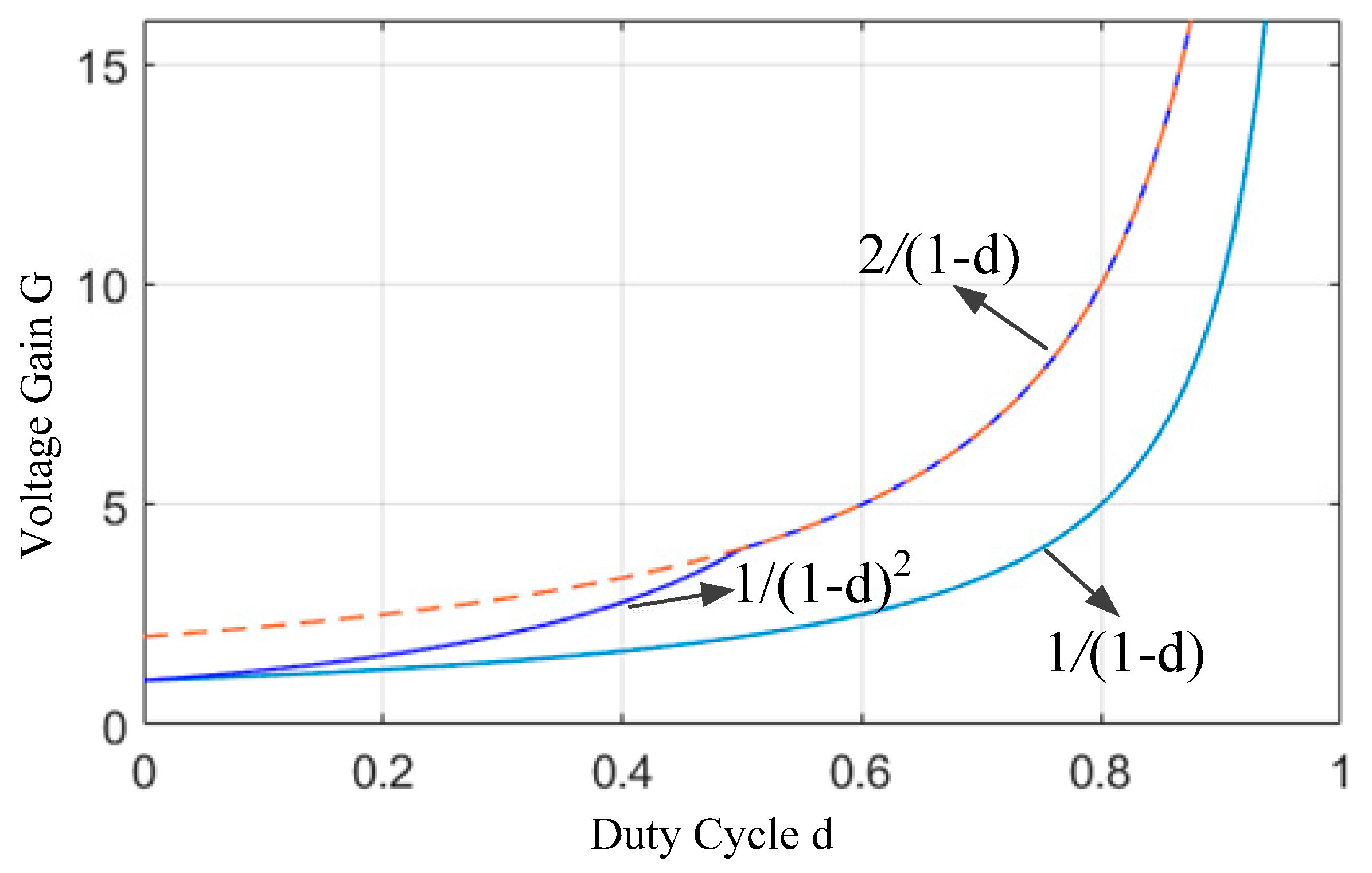
3.5. Comparative Analysis

Comparative analyses of SC-TLB, SI-TLB, SI-FC-TLB, PI-FC-TLB and the proposed IPOS-SC-TLB are presented in Table 2. L, S, D, and C represent the quantities of inductors, switches, diodes and capacitors, respectively. DS means the quantity of driver supplies and G means the voltage gains. Besides, UVPS, UVPD, and UVPC respectively represent the voltage stresses across switches, diodes, capacitors; and IVPS1, IVPS2, and IVPD represent the average current across switches S1, S2 and diodes, respectively. “Self-balance” means the input inductor currents could be self-balanced and “same ground” means the input terminal and the output terminal share the same ground. In addition, the voltage gain comparison curves are presented in Figure 9.
Among these seven TLB converters, the common performance parameters are the voltage stress across switches and the input current ripple. The TLB converters based on SI structure need two isolated drive power supplies and have a low voltage gain, while those TLB converters based on PI structure need only one power supply and show a higher voltage gain. The SI-FC-TLB and PI-FC-TLB are very similar except for different interleaved structures. From these two converters, it could be seen that the voltage stresses across the output diodes are low in the SI structure while high in the PI structure; and the average current stresses across switches are high in the SI structure while low in the PI structure. The smaller average current stress across switches should be attributed to the PI structure. Among the five converters, the quantity of components are not the most in the proposed IPOS-SC-TLB, and high voltage gain, small voltage stress and small current stress are achieved. Moreover, voltage-balance control could be easily achieved with the input terminal and the output terminal sharing the same ground. In other words, the proposed IPOS-SC-TLB converter integrates nearly all the merits of the other four TLB converters. However, there is also a disadvantage that the imbalance current between the two power switches S1, S2. As analyzed in Equation (28), the average current of S2 is Uo/R higher than the average current of S1.

4. Three-Loop Control Strategy

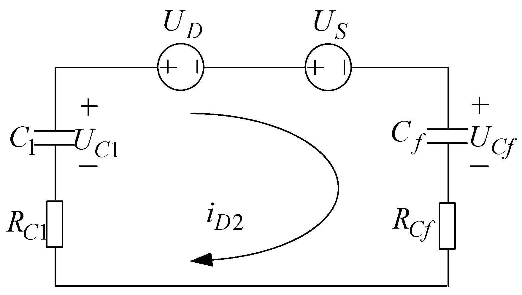
4.1. Voltage Imbalance Mechanism

η 1 , η 2 are labelled as the conversion efficiencies of Boost I and Boost II, respectively. Thus, there is:
{ η 1 U i n I L 1 = U C 1 I D 1 η 2 U i n I L 2 = U C 2 I D 3  
As the output terminals of Boost I and Boost II are connected in series, the two Boost modules have the same output current. As the average currents across C1 and C2 are both equal to zero during one switching period, there is:
I D 1 = I D 3  
In addition, the power losses of D2 and S2 produced in the switched-capacitor network are small but could not be ignored. But the power losses should be attributed to the Boost II as D2 and S2 help formulate the Boost II. As a result, there is:
η 1 > η 2  
Based on (36)–(38), we have:
U C 1 > U C 2  
As analyzed above, the two split inductor currents could be self-balanced, but the two output capacitor voltages could not be self-balanced. Considering the voltage drops of IGBT and diode, the voltage difference between C1 and C2 could be described by the sum of the voltage drop of one IGBT and the voltage drop of one diode. Besides, the parasitic resistances of L1 and L2 are labelled as rL and the parasitic resistance of Cf is labelled as rCf. As the average currents across L1 and L2 are high, the voltage drops of parasitic resistances are large and could not be ignored. Under this condition, the two output capacitor voltages could be rewritten as:
U C 1 = 1 1 d ( U i n I L 1 r L ) U D  
U C 2 = 1 1 d [ U i n I L 2 ( r L + r C f ) ] Δ U U D  
The two split inductors are designed to attain the same parameters. Owing to the automatic balanced inductor currents, the voltage difference between C1 and C2 could be described by:
Δ U = U C 1 U C 2 = I L 2 r C f 1 d + Δ U  
Considering (15)–(42) is further simplified as:
Δ U = U C 1 U C 2 = I L 2 r C f + Δ U S C 1 d = I i n r C f 2 ( 1 d ) + U S + U D  
It can be seen from (43) that the voltage imbalance issue is related to the output characteristic and the parasitic parameters, including the average input current Iin, the duty cycle d, the equivalent series resistance rCf of the flying-capacitor, and the voltage drops of IGBTs and diodes. The capacitances of the two output capacitors have no effect on the voltage imbalance issue, which is quite different from the conventional three-level boost converter shown in Figure 2a.

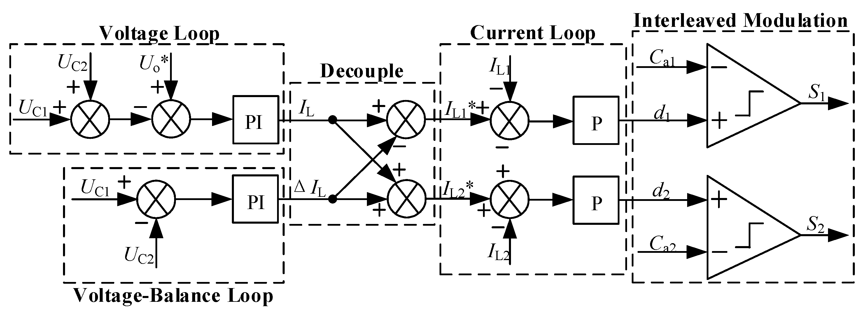
4.2. Three-Loop Control Strategy

To address the voltage imbalance issue and to achieve stale operation of the IPOS-SC-TLB converter, a three-loop control strategy including an output voltage loop, an input current loop and a voltage-balance loop is proposed in this section. The voltage loop and the current loop respectively controls the output voltage and the input inductor currents, while the voltage-balance loop helps alleviate the voltage imbalance issue. However, the voltage loop and the voltage-balance loop will influence each other if no decoupling scheme is employed. To decouple the output voltage loop and the voltage-balance loop, the derivation analysis has been done as follows.
Duty cycles d1, d2 in (44) are both composed of the common duty cycle d and the voltage-balance duty cycles Δd1, Δd2. Also, IL1, IL2 in (45) are both composed of the average inductor current IL and the voltage-balance inductor current ΔIL1, ΔIL2:
{ d 1 = d + Δ d 1 d 2 = d + Δ d 2  
{ I L 1 = I L + Δ I L 1 I L 2 = I L + Δ I L 2  
In the IPOS-SC-TLB converter, the relationship of the input inductor currents and the output current could be described by:
{ ( 1 d 1 ) I L 1 = I o ( 1 d 2 ) I L 2 = I o  
By substituting (44) and (45) into (46), there is:
{ ( 1 d ) Δ I L 1 Δ d 1 I L = Δ I o ( 1 d ) Δ I L 2 Δ d 2 I L = Δ I o  
When the output voltage is not disturbed, the output current variation ΔIo is equal to zero. Thus, (47) could be simplified by:
{ Δ d 1 = 1 d I L Δ I L 1 Δ d 2 = 1 d I L Δ I L 2  
When the IPOS-SC-TLB converter works at stable steady state, ΔIL1 and ΔIL2 indirectly reflect the values of Δd1, Δd2. According to (38), it is not difficult to deduce the following formula:
Δ I L 1 + Δ I L 2 = I L 1 d ( Δ d 1 + Δ d 2 )  
In the three-loop control strategy, to decouple the voltage loop and the voltage-balance loop, the sum of Δd1 and Δd2 should be equal to zero. Thus, according to (49), there is:
Δ I L 1 + Δ I L 2 = 0  
Then, the reference inductor currents of Boost I and Boost II could be concluded as follows:
{ I L 1 = I L + Δ I L 1 = I L Δ I L I L 2 = I L + Δ I L 2 = = I L + Δ I L  
According to (51), the three-loop control strategy is presented in Figure 10. The regulators of the output voltage loop and the voltage-balance loop adopt proportional-integral controller while the regulator of the current loop adopts proportional controller. The controllers can be designed based on a small-signal linearized model of the dc/dc converter, which can be developed according to the classic average modeling method for power converters [35,36]. The inner current control loop is designed to respond faster than the outer voltage control loop so that the two control loops can be designed independently. As a result, when dealing with the inner loop, we take the outer loop as a constant input. On the other hand, the inner current control loop can be approximated as a simple lag block when we proceed with the voltage loop. The voltage-balance loop has the slowest response. When designing the controller for the voltage-balance loop, the voltage and current control loop can be considered being in steady state already. Classic Bode-plot and root-locus proportional-integral controller design procedures [36] can be used to obtain the parameters for the controllers. Nevertheless, it should be noted that due to the nonlinearity of power devices, the designed controller parameters need to be further tuned for the actual circuit. Besides, the carrier signals Ca1, Ca2 are with phase-shifted 180 degrees to realize interleaved scheme for the switches S1 and S2.
The two sampled capacitor voltages UC1, UC2 are added together and then compared with the output voltage reference Uo* to output the average inductor current IL through the voltage loop regulator. ΔIL is achieved through the voltage-balance loop regulator by comparing UC1 and UC2. ΔIL2 equals to −ΔIL1 according to (50). The inductor current references IL1*, IL2* in (51) could be achieved through the decoupled scheme. Then, IL1* and IL2* compares with IL1 and IL2, and pass though the two current loop regulators to output the duty cycles of Boost I and Boost II as follows:
{ d 1 = d + Δ d 1 = d Δ d d 2 = d + Δ d 2 = d + Δ d  
When UC1 is bigger than UC2, the voltage-balance process is: ΔIL becomes positive, which makes IL1* decrease and IL2* increase. As a result, d1 decreases while d2 increases, i.e., the turn-on time of S1 decreases while that of S2 increases. Thus, UC1 decreases while UC2 increases. Finally, UC1 equals to UC2 after several switching periods. When UC1 is smaller than UC2, UC1 and UC2 could be also balanced according to a similar voltage-balance process.

5. Simulation and Experimental Verification

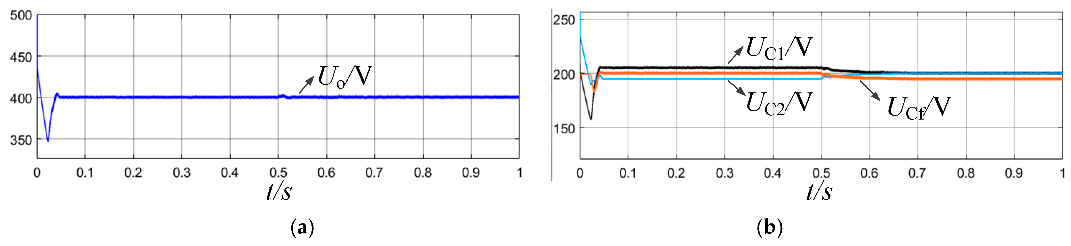
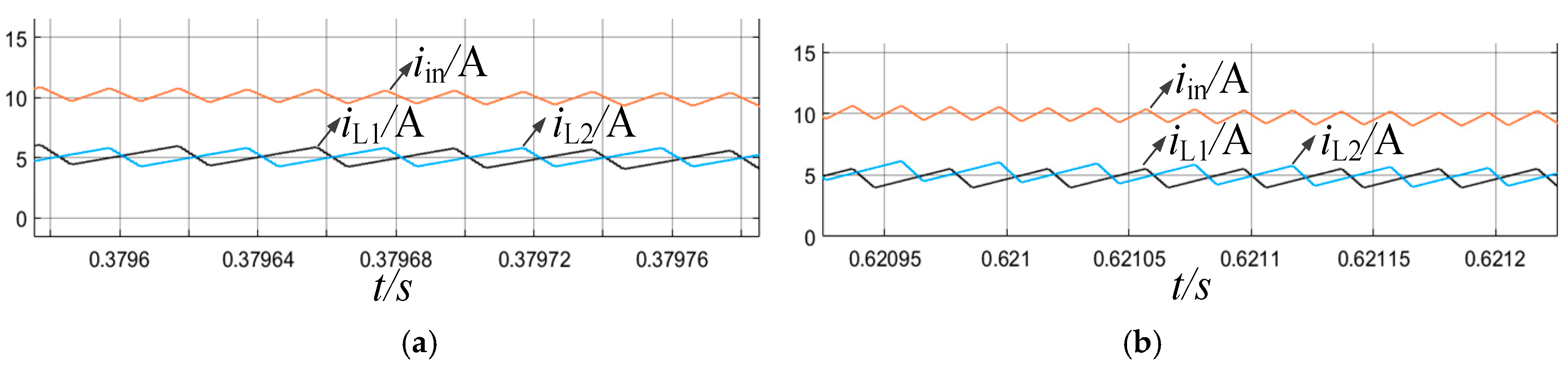
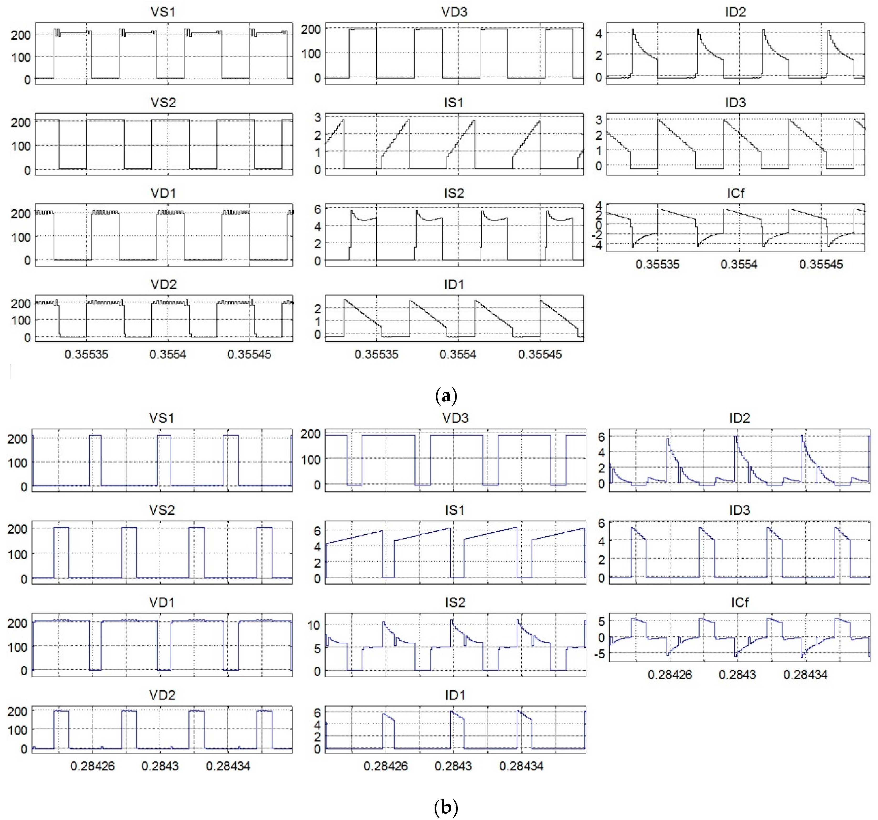
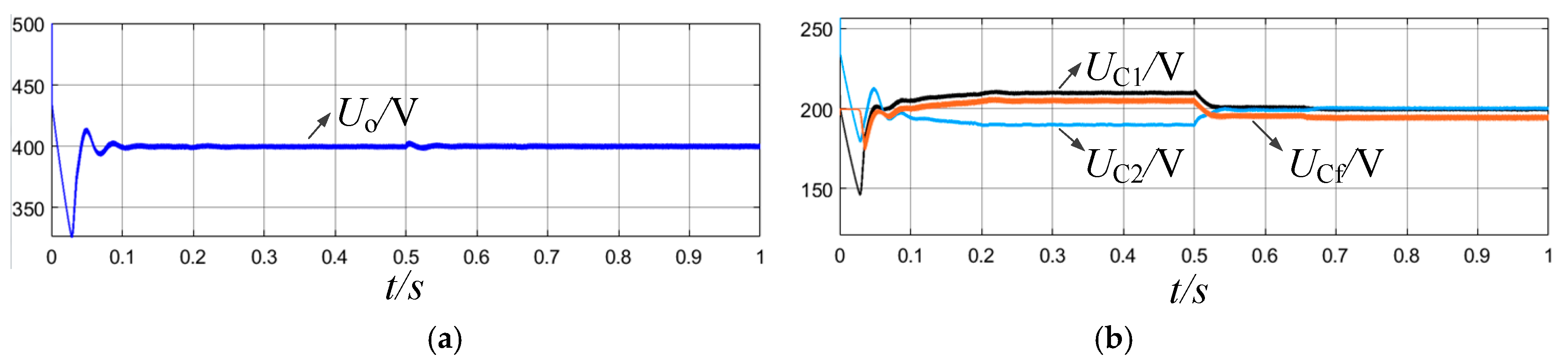
5.1. Simulation Verification

To verify the correctness and feasibility of the IPOS-SC-TLB converter, a simulation model adopting the proposed three-loop control strategy with 400 W output power has been implemented. The detailed simulation and experimental parameters are presented in Table 3.
The input voltage varies between 48 V and 120 V, and the output voltage is controlled to be stable at 400 V. The switching frequency of the converter is set as 25 kHz. Two inductors are both chosen as about 900 μH with 0.1 ohm equivalent series resistance. Three capacitors are all set as 470 μF with 0.28 ohm equivalent series resistance. Each of the two IGBT switches has a voltage drop of 2.4 V and each of the three diodes has a voltage drop of 2.0 V. Figure 11 shows the simulation results when the input voltage is 48 V and Figure 12 shows the simulation results when the input voltage is 120 V. It can be seen that the IPOS-SC-TLB converter can output a stable dc voltage of 400 V under both the two different input voltages. The voltage difference between UC1 and UC2 is about 20 V under the input voltage 48 V and 10 V under the input voltage 120 V without voltage-balance control. However, once the voltage-balance control loop is added, UC1 and UC2 are balanced with the same voltage 200 V. Besides, in the whole experimental process, a small voltage difference between UC1 and UCf is about 4.4 V, which is the sum of the voltage drop of one IGBT and the voltage drop of one diode.
More importantly, Figure 13 shows the two split inductor current waveforms of the converter without voltage-balance control and with voltage-balance control when the input voltage is 48 V. Under the condition without voltage-balance control, the average values of the two inductor currents are equal while a little different under the condition with voltage-balance control. Because the duty cycle d1 and the duty cycle d2 are the same under the condition without voltage-balance control but d1 is a little smaller than d2 under the condition with voltage-balance control. Besides, the input current ripple is smaller than the inductor current ripples, and input current ripple frequency is 50 kHz, which is two times the switching frequency 25 kHz.
The simulated voltage waveforms and current waveforms are presented in Figure 14. The voltage stress across all power devices are half of the output voltage. The average current across every diode is 1 A, which is the same as the output current. Additionally, the average current across the switch S2 is bigger than S1 because the current across the diode D2 added on the current of S2. These results prove correctness of the theoretically derived results shown in (28). On the whole, the simulation results basically verify the effectiveness of the IPOS-SC-TLB converter and the proposed three-loop control strategy.

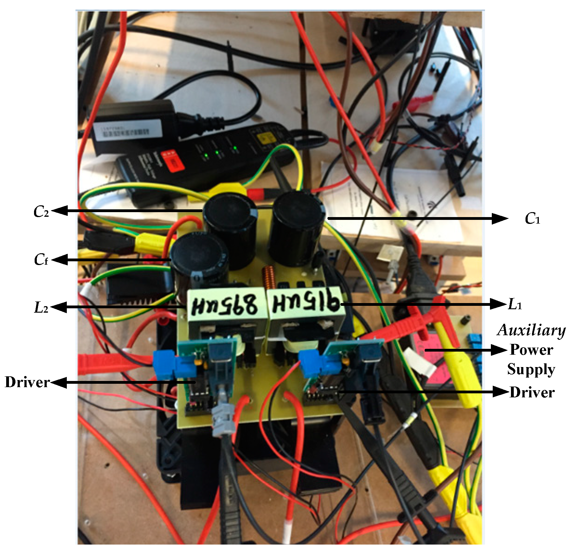
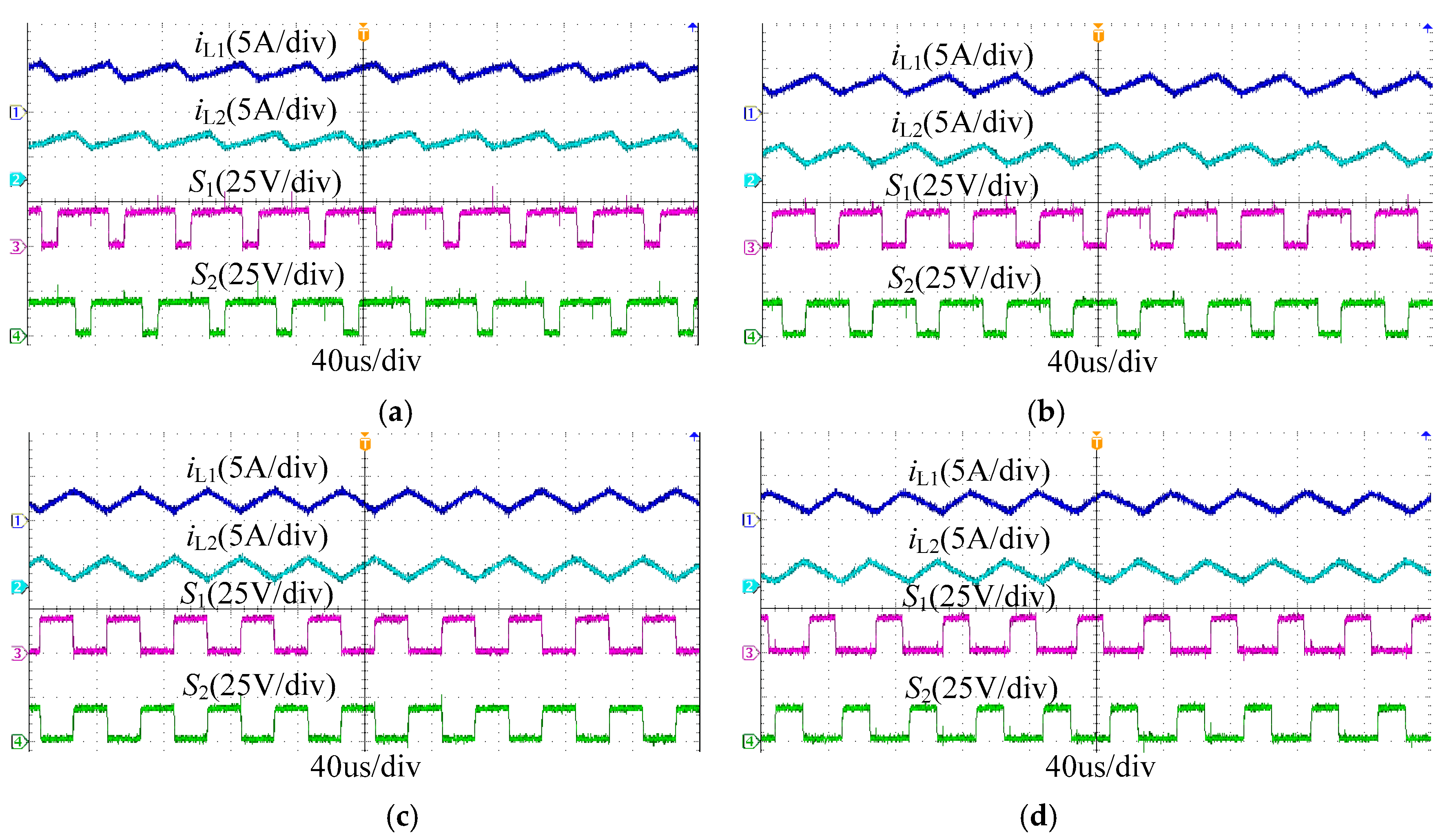
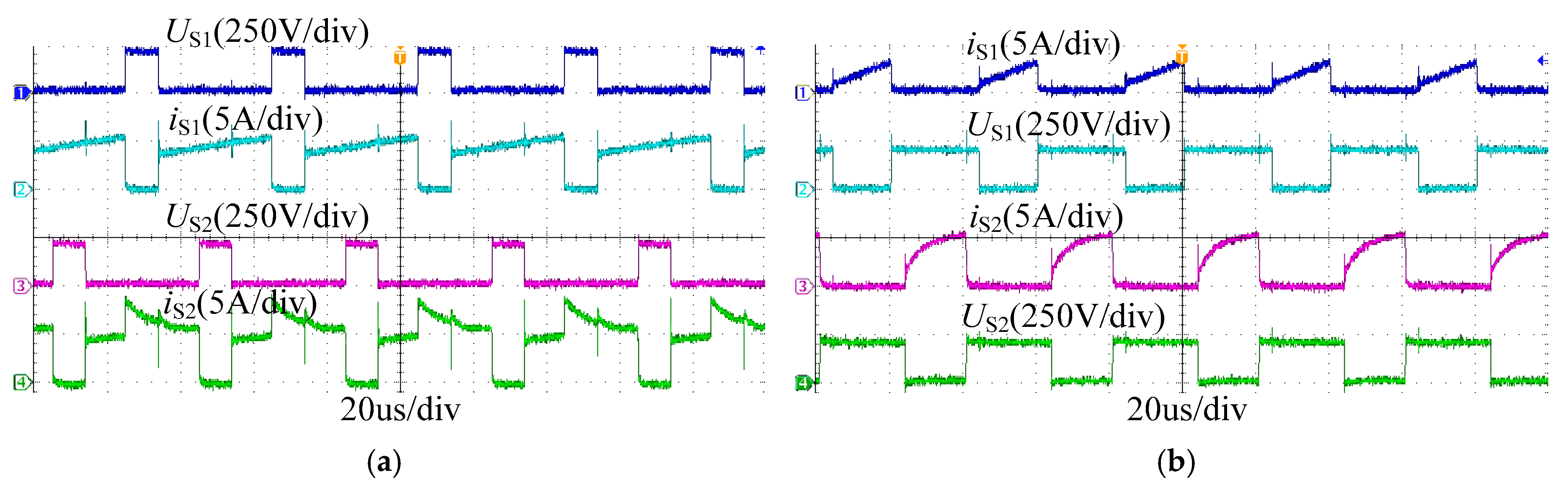
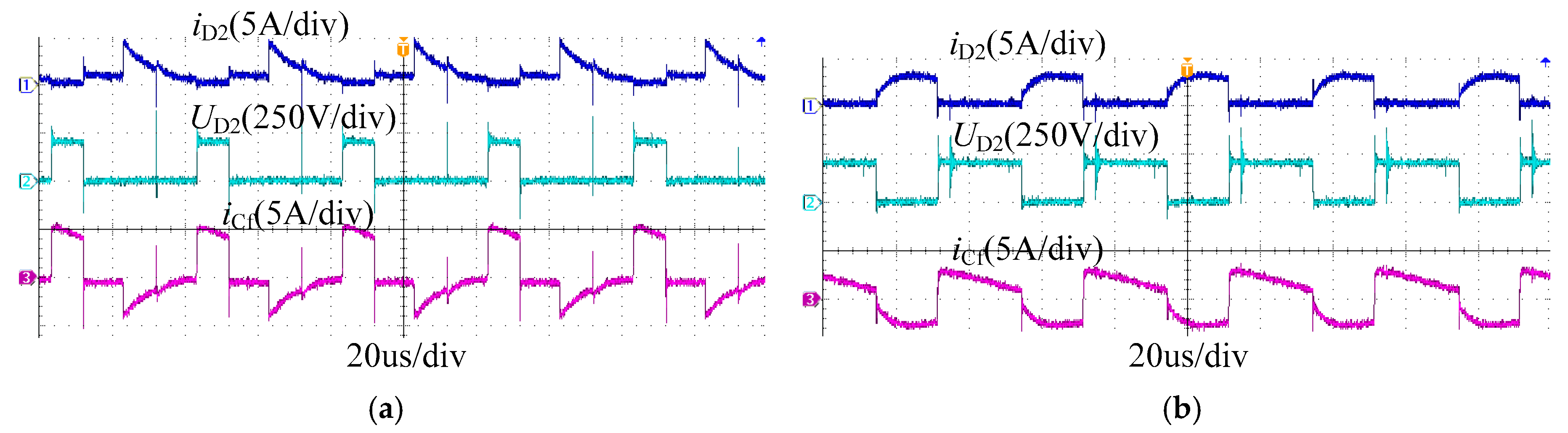
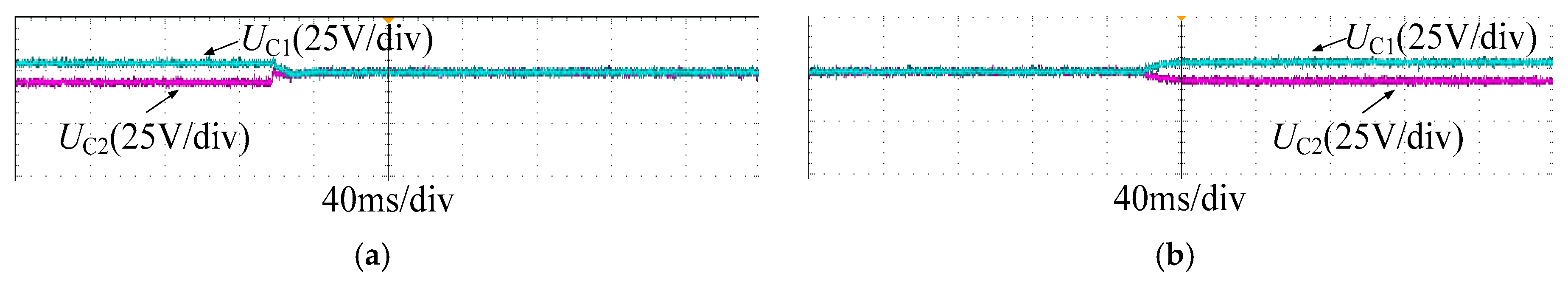
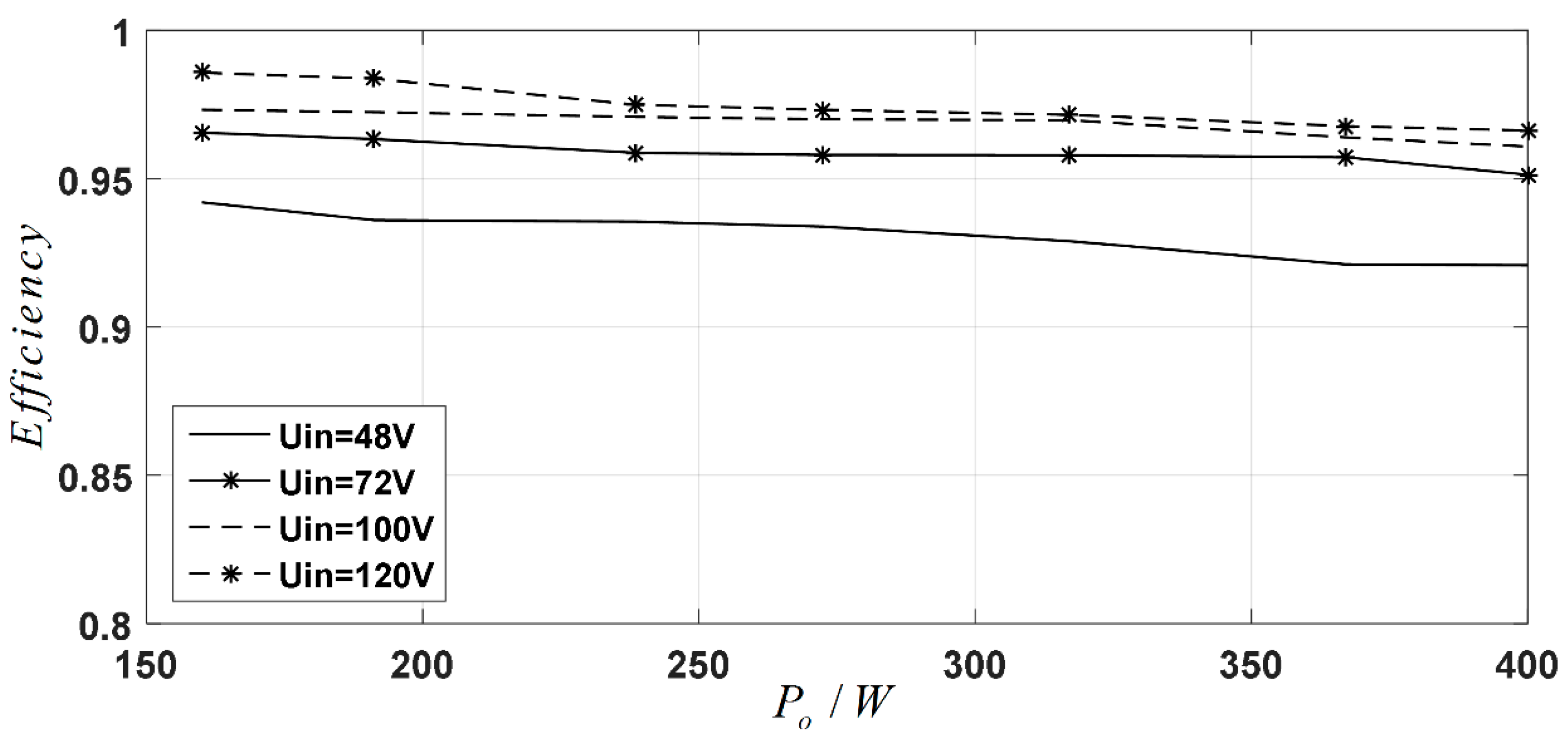
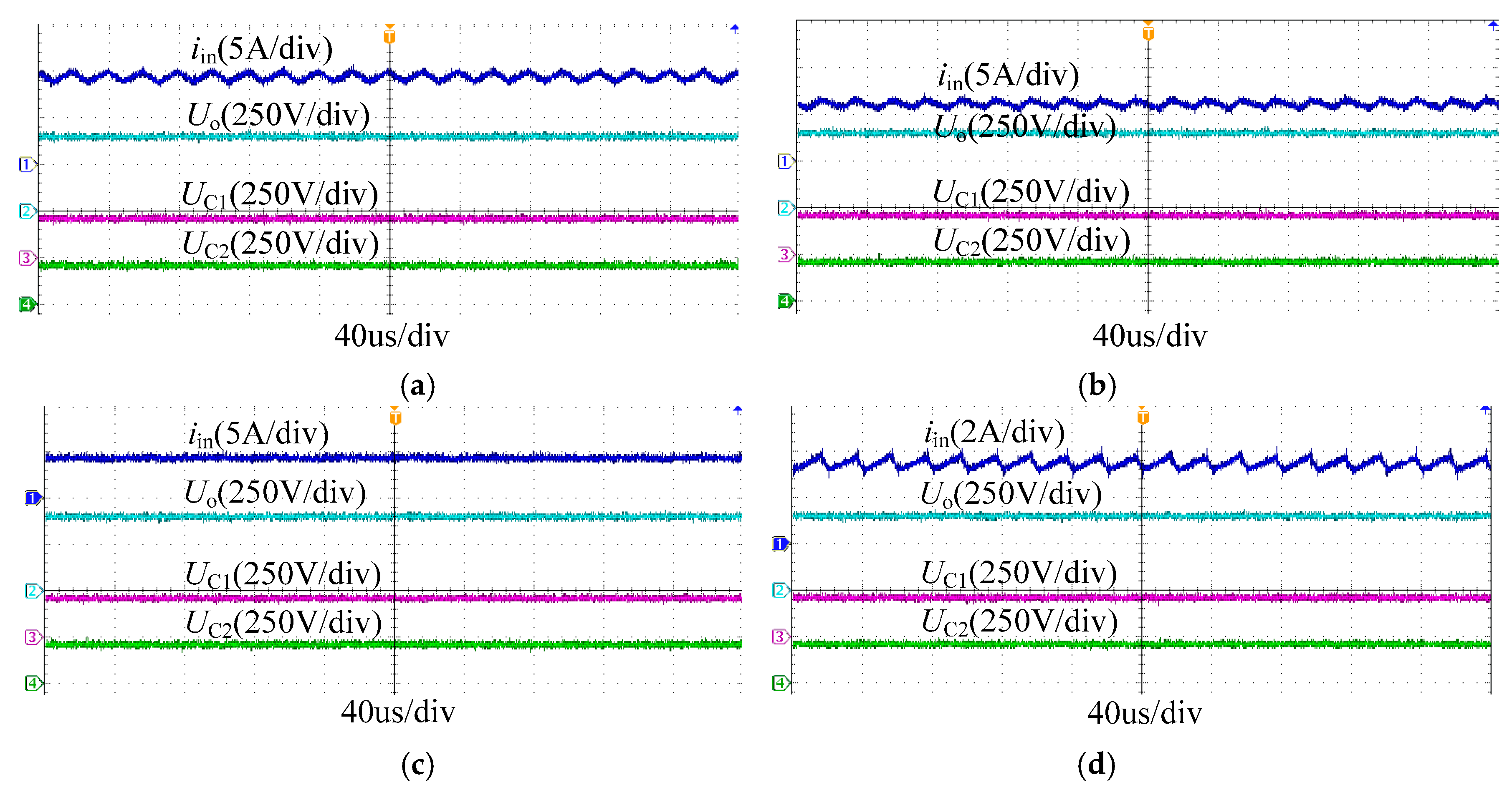
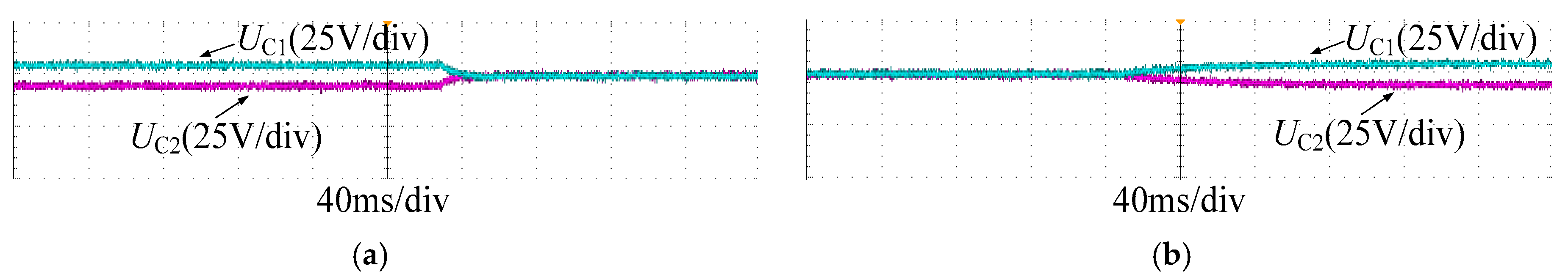
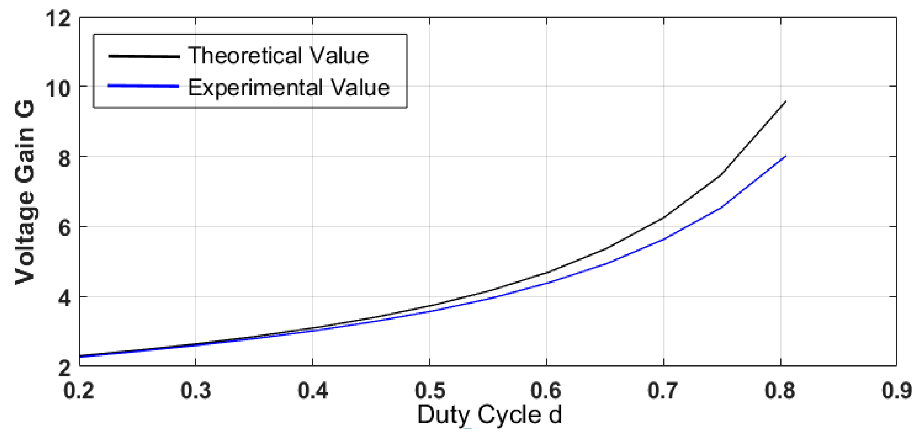
5.2. Experimental Verification

To verify the converter and three-loop control strategy further, an experimental prototype with the same parameters shown in simulation model is built and it is given in Figure 15. It should be noted that the inductors L1, L2 are respectively designed to be 915 μH, 895 μH with some deviations in fact. The two switches are both selected as IGBT G80N60, which have a voltage drop of 2.4 V and the three diodes are selected as DSEP30-06B, which have a voltage drop of 2.0 V. The control loop of the converter was implemented based on Dspace 1103.
The input current and capacitor voltages of the IPOS-SC-TLB converter under different input voltages are presented in Figure 16, and the corresponding capacitor voltages are presented in Figure 17. The inductor currents across L1, L2 and the drive signals of S1, S2 are presented in Figure 18. It can be seen that the output voltage is stable at 400 V and the three capacitor voltages are stable with 200 V under different input voltages. The input current is continuous with a small current ripple and the input current ripple frequency is 50 kHz, which is two times the switching frequency 25 kHz. Moreover, it is easy to observe that as the duty cycle approaches 0.50, the input current ripple becomes almost zero, which verifies (32).
To show voltage stresses across all the switches and diodes, the terminal voltage waveforms of S1, S2, D1, D2, and D3 are presented in Figure 19, Figure 20 and Figure 21. It should be noted that uS1, uS2 are defined to describe the voltage difference between the drain terminal and the source terminal of S1 and S2, respectively. uD1, uD2, uD3 are the voltage differences between the cathode and the anode of D1, D2 and D3. It can be seen that all the voltage stresses of the switches and diodes are 200 V, which is half of the output voltage 400 V. It matches with (12). In addition, the current IS2 is the sum of IS1 and ID2, which matches with (20) and (21). For example, when the input voltage is 48 V, IS1, IS2, ID2 are 3.74 A, 4.78 A and 1.13 A, respectively. It is not difficult to know that the switching state of D1 is complementary to that of D2, and the switching state of D1 is 180 degrees shifted from that of D3. The switching state of S1 is also 180 degrees shifted from that of S2. All of these results can verify the correctness of the operating principle of the IPOS-SC-TLB converter.
More importantly, the voltage-balance experimental waveforms of the IPOS-SC-TLB converter are presented in Figure 22 and Figure 23. The experimental results indicate that when the voltage-balance loop is not added, there is about 13.0 V voltage difference between UC1 and UC2. For example, when the input voltage is 48 V, the tested duty cycle is around 0.83. According to (43), the voltage difference between UC1 and UC2 is 11.26 V under the input voltage of 48 V. The tested voltage difference of 13.00 V basically matches the theoretical value 11.26 V with some voltage error. When the voltage-balance loop is added, the voltage difference becomes nearly zero.
Figure 24 shows the theoretical voltage gain and the experimental voltage gain versus duty cycle when Uin is 48 V. It can be seen that the theoretical voltage gain and the experimental voltage gain have the same increasing trend though some deviations exist. The experimental voltage gain basically matches the theoretical voltage gain when the duty cycle varies between 0.2 and 0.5. However, when the duty cycle is over 0.50, the experimental theoretical voltage gain is less than the theoretical voltage gain, and their difference increases with the duty-cycle increasing. This phenomenon may be due to the non-linearity of power electronic components and the fact the true values of parasitic parameters are hard to obtain.
The conversion efficiency curves versus output power for the IPOS-SC-TLB converter under different input voltages are given in Figure 25. The minimum efficiency and the maximum efficiency are 92.08% and 94.20%, respectively, at an input voltage of 48 V; 95.13% and 96.55% at the input voltage of 72 V; 96.08% and 97.32% at the input voltage 100 V; 96.62% and 98.57% at an input voltage of 120 V. It can be seen that the proposed converter is not efficient in low voltage levels, such as 48 V in the experiment. To make it efficient, the converter should be implemented with optimized design, including component selection, coupling inductor design and applying soft switching technique. For component selection, wide bandgap device (SiC, GaN) with much smaller parasitic parameters should be a good solution, which could not only reduce conduction and switching losses, but also enhance the switching frequency to reduce passive components’ size and parasitic parameters as well. Coupling design for the two inductors L1 and L2 will help reduce size and improve efficiency of the converter. Soft switching technique applied on this converter will help enhance conversion efficiency.
Based on all the experimental results, the theoretical analysis of the IPOS-SC-TLB converter is correct and the three-loop control strategy is feasible. The effectiveness of the proposed IPOS-SC-TLB converter has been verified.

6. Conclusions

This paper presents an input-parallel-output-series three-level Boost converter, which can step up the input voltage to a high voltage level, as well as attaining low voltage stress, low current stress and small input current ripple. Another advantage of the proposed topology is the automatic current balancing function. There is also a disadvantage that the imbalance current between the two power switches S1, S2. The average current of S2 is Uo/R higher than the average current of S1.

Author Contributions

J.C. proposed the topology and control strategy, and built the simulation model and experimental prototype. C.W. and J.L. helped do comparative analysis and wrote the paper.

Funding

This research was funded by China Postdoctoral Science Foundation, grant number 2017M612908.

Conflicts of Interest

The authors declare no conflict of interest.

Nomenclature

List of Abbreviations
IPOS-SC-TLBinput-parallel-output-series switched-capacitor three-level boost
HVDChigh voltage direct current
SIserial-interleaved
PIparallel-interleaved
SI-TLBserial-interleaved three-level boost
PIBparallel-interleaved boost
SI-FC-TLBserial-interleaved flying-capacitor three-level boost
PI-FC-TLBparallel-interleaved flying-capacitor three-level boost
PI-SFC-TLBparallel-interleaved symmetric flying-capacitor three-level boost
SC-TLBswitched-capacitor three-level boost
IPOS-TLB1input-parallel-output-series three-level boost 1
IPOS-TLB2input-parallel-output-series three-level boost 2
List of Symbols
Uinaverage input voltage
Uo, Ioaverage output voltage and average output current
Uo*output voltage reference
UC1, UC2, UCfaverage voltages of capacitors C1, C2, Cf
ΔUvoltage difference between C1 and Cf,
iL1, iL2currents of inductors L1, L2
IL1, IL2average currents of inductors L1, L2
IL1*, IL2*reference currents of inductors L1, L2
ΔiL1, ΔiL2current ripples of inductors L1, L2
Δiininput current ripple
ID1, ID2, ID3average currents of diodes D1, D2, D3
IS1, IS2average currents of switches S1, S2
dduty cycle
d1duty cycle of boost 1
d2duty cycle of boost 2
Δdduty cycle difference

References

  1. Yaramasu, V.; Wu, B.; Sen, P.C.; Kouro, S.; Narimani, M. High-power Wind Energy Conversion Systems: State-of-the-art and Emerging Technologies. Proc. IEEE 2015, 103, 740–788. [Google Scholar] [CrossRef]
  2. Yaramasu, V.; Wu, B. Predictive Control of a Three-Level Boost Converter and an NPC Inverter for High-Power PMSG-Based Medium Voltage Wind Energy Conversion Systems IEEE Trans. Power Electron. 2014, 29, 5308–5322. [Google Scholar] [CrossRef]
  3. Parastar, A.; Seok, J.-K. High Power Step-Up Modular Resonant DC/DC Converter for Offshore Wind Energy Systems. IEEE Energy Convers. Congr. Expos. (ECCE) 2014, 3341–3348. [Google Scholar] [CrossRef]
  4. Yaramasu, V.; Wu, B.; Rivera, M.; Rodriguez, J. A New Power Conversion System for Megawatt PMSG Wind Turbines Using Four-Level Converters and a Simple Control Scheme Based on Two-Step Model Predictive Strategy-Part I: Modeling and Theoretical Analysis. IEEE J. Emerg. Sel. Top. Power Electron. 2014, 2, 3–13. [Google Scholar] [CrossRef]
  5. Paez, J.D.; Frey, D.; Maneiro, J.; Bacha, S.; Dworakowski, P. Overview of DC-DC Converters Dedicated to HVDC Grids. IEEE Trans. Power Deliv. 2018. [Google Scholar] [CrossRef]
  6. Xia, C.; Gu, X.; Shi, T.; Yan, Y. Neutral-Point Potential Balancing of Three-Level Inverters in Direct-Driven Wind Energy Conversion System. IEEE Trans. Energy Convers. 2011, 26, 18–29. [Google Scholar] [CrossRef]
  7. Chen, J.; Wang, C.; Li, J.; Jiang, C.; Duan, C. A Nonisolated Three-Level Bidirectional DC-DC Converter. In Proceedings of the 2018 IEEE Applied Power Electronics Conference and Exposition (APEC), San Antonio, TX, USA, 4–8 March 2018; pp. 1566–1570. [Google Scholar]
  8. Hou, S.; Chen, J.; Sun, T.; Bi, X. Multi-input Step-Up Converters Based on the Switched-Diode-Capacitor Voltage Accumulator. IEEE Trans. Power Electron. 2016, 31, 381–393. [Google Scholar] [CrossRef]
  9. Zhou, H.; Zhou, J.; Hu, B.; Tong, C. A New Interleaved Three-level Boost Converter and Neutral-point Potential Balancing. In Proceedings of the 2013 2nd International Symposium on Instrumentation and Measurement, Sensor Network and Automation (IMSNA), Toronto, ON, Canada, 23–24 December 2013. [Google Scholar]
  10. Zhang, Y.; Sun, J.-T.; Wang, Y.-F. Hybrid Boost Three-Level DC-DC Converter With High Voltage Gain for Photovoltaic Generation Systems. IEEE Trans. Power Electron. 2013, 28, 3659–3664. [Google Scholar] [CrossRef]
  11. Andrade, A.M.S.S.; Martins, M.L.D.S. Quadratic-Boost with Stacked Zeta Converter for High Voltage Gain Applications. IEEE J. Emerg. Sel. Top. Power Electron. 2017, 5, 1787–1796. [Google Scholar] [CrossRef]
  12. Jin, K.; Yang, M.; Ruan, X.; Xu, M. Three-Level Bidirectional Converter for Fuel-Cell/Battery Hybrid Power System. IEEE Trans. Ind. Electron. 2010, 57, 1976–1986. [Google Scholar] [CrossRef]
  13. Rahul, J.R.; Kirubakaran, A.; Vijayakumar, D. A New Multilevel DC-DC Boost Converter for Fuel Cell based Power System. In Proceedings of the 2012 IEEE Students’ Conference on Electrical, Electronics and Computer Science (SCEECS), Bhopal, India, 1–2 March 2012. [Google Scholar]
  14. Hegazy, O.; Mierlo, J.V.; Lataire, P. Analysis, Modeling, and Implementation of A Multidevice Interleaved DC/DC Converter for Fuel Cell Hybrid Electric Vehicles IEEE Trans. Power Electron. 2012, 27, 4445–4458. [Google Scholar] [CrossRef]
  15. Ni, L.; Patterson, D.J.; Hudgins, J.L. High Power Current Sensorless Bidirectional 16-Phase Interleaved DC-DC Converter f or Hybrid Vehicle Application. IEEE Trans. Power Electron. 2012, 27, 1141–1151. [Google Scholar] [CrossRef]
  16. Rivera, S.; Wu, B.; Kouro, S.; Yaramasu, V.; Wang, J. Electric Vehicle Charging Station Using A Neutral-point Clamped Converter with Bipolar DC Bus. IEEE Trans. Ind. Electron. 2015, 62, 1999–2009. [Google Scholar] [CrossRef]
  17. Tan, L.; Wu, B.; Yaramasu, V.; Rivera, S.; Guo, X. Effective Voltage Balance Control for Bipolar-DC-Bus Fed EV Charging Station with Three-Level DC-DC Fast Charger. IEEE Trans. Ind. Electron. 2016, 63, 4031–4041. [Google Scholar] [CrossRef]
  18. Adam, G.P.; Gowaid, I.A.; Finney, S.J.; Holliday, D.; Williams, B.W. Review of DC-DC Converters for Multi-terminal HVDC Transmission Networks. IET Power Electron. 2016, 9, 281–296. [Google Scholar] [CrossRef] [Green Version]
  19. Chen, J.; Hou, S.; Deng, F.; Chen, Z. An Interleaved Five-Level Boost Converter with Voltage-Balance Control. J. Power Electron. 2016, 16, 1735–1742. [Google Scholar] [CrossRef]
  20. Kakigano, H.; Miura, Y.; Ise, T. Distribution Voltage Control for DC Microgrids Using Fuzzy Control and Gain-Scheduling Technique. IEEE Trans. Power Electron. 2013, 28, 2246–2258. [Google Scholar] [CrossRef]
  21. Jang, Y.; Jovanovic, M.M. Interleaved Boost Converter with Intrinsic Voltage-Doubler Characteristic for Universal-Line PFC Front End. IEEE Trans. Power Electron. 2007, 22, 1394–1401. [Google Scholar] [CrossRef]
  22. Zhou, L.-W.; Zhu, B.-X.; Luo, Q.-M.; Chen, S. Interleaved Non-isolated High Step-up DC-DC Converter Based on the Diode-capacitor Multiplier. IET Power Electron. 2014, 7, 390–397. [Google Scholar] [CrossRef]
  23. Franco, L.C.; Pfitscher, L.L.; Gules, R. A New High Static Gain Nonisolated DC-DC Converter. In Proceedings of the 34th Annual Power Electronics Specialist Conference IEEE, Acapulco, Mexico, 15–19 June 2003. [Google Scholar]
  24. Kajangpan, K.; Neammenee, B. High Gain Double Interleave Technique with Maximum Peak Power Tracking for Wind Turbine Converter. In Proceedings of the 2009 6th International Conference on Electrical Engineering/Electronics, Computer, Telecommunications and Information Technology Pattaya, Chonburi, Thailand, 6–9 May 2009. [Google Scholar]
  25. Forest, F.; Huselstein, J.J.; Martiré, T.; Flumian, D.; Meynard, T.A.; Abdelli, Y.; Lienhardt, A.M. A Nonreversible 10-kW High Step-Up Converter Using a Multicell Boost Topology. IEEE Trans. Power Electron. 2018, 33, 151–160. [Google Scholar] [CrossRef]
  26. Rosas-Caro, J.C.; Ramirez, J.M.; Peng, F.Z.; Valderrabano, A. A DC-DC Multilevel Boost Converter. IET Power Electron. 2010, 3, 129–137. [Google Scholar] [CrossRef]
  27. Parastar, A.; Kang, Y.C.; Seok, J.-K. Multilevel Modular DC-DC Power Converter for High-Voltage DC-Connected Offshore Wind Energy Applications. IEEE Trans. Ind. Electron. 2015, 62, 2879–2890. [Google Scholar] [CrossRef]
  28. Zhang, X.; Green, T.C. The Modular Multilevel Converter for High Step-Up Ratio DC-DC Conversion. IEEE Trans. Ind. Electron. 2015, 62, 4925–4936. [Google Scholar] [CrossRef]
  29. Ferreira, J.A. The Multilevel Modular DC Converter. IEEE Trans. Power Electron. 2013, 28, 4460–4465. [Google Scholar] [CrossRef]
  30. Zhang, X.; Green, T.C. The New Family of High Step Ratio Modular Multilevel DC-DC Converters. In Proceedings of the 2015 IEEE Applied Power Electronics Conference and Exposition (APEC), Charlotte, NC, USA, 15–19 March 2015. [Google Scholar]
  31. Hagar, A.A.; Lehn, P.W. Comparative Evaluation of a New Family of Transformerless Modular DC-DC Converters for High-Power Applications. IEEE Trans. Power Deliv. 2014, 29, 444–452. [Google Scholar] [CrossRef]
  32. Filsoof, K.; Lehn, P.W. A Bidirectional Modular Multilevel DC-DC Converter of Triangular Topology. IEEE Trans. Power Electron. 2015, 30, 54–64. [Google Scholar] [CrossRef]
  33. Athab, H.; Yazdani, A.; Wu, B. A Transformerless DC-DC Converter with Large Voltage Ratio for MV DC Grids. IEEE Trans. Power Deliv. 2014, 29, 1877–1885. [Google Scholar] [CrossRef]
  34. Chen, W.; Huang, A.Q.; Li, C.; Wang, G.; Gu, W. Analysis and Comparison of Medium Voltage High Power DC-DC Converters for Offshore Wind Energy Systems. IEEE Trans. Power Electron. 2013, 28, 2014–2023. [Google Scholar] [CrossRef]
  35. Mohan, T.; Undeland, M.; Robbins, W.P. Power Electronics—Converters, Applications, and Design; John Wiley & Sons Inc.: Hoboken, NJ, USA, 2003. [Google Scholar]
  36. Erickson, R.W.; Maksimovic, D. Fundamentals of Power Electronics, 2nd ed.; Kluwer Academic Publisher: Norwell, MA, USA, 2001. [Google Scholar]
Figure 1. Two interleaved structures: (a) SI; (b) PI.
Energies 11 02631 g001
Figure 2. Development of TLB converters: (a) SI-TLB; (b) PIB; (c) SI-FC-TLB; (d) PI-FC-TLB; (e) PI-SFC-TLB; (f) SC-TLB; (g) IPOS-TLB1; (h) IPOS-TLB2.
Energies 11 02631 g002aEnergies 11 02631 g002b
Figure 3. The proposed IPOS-SC-TLB converter.
Energies 11 02631 g003
Figure 4. Equivalent circuits of the IPOS-SC-TLB converter: (a) stage I; (b) stage II; (c) stage III; (d) stage IV.
Energies 11 02631 g004
Figure 5. Key voltage waveforms: (a) d > 0.5; (b) d ≤ 0.5.
Energies 11 02631 g005
Figure 6. Key current waveforms: (a) d > 0.5; (b) d ≤ 0.5.
Energies 11 02631 g006
Figure 7. Equivalent circuit of the switched-capacitor network.
Energies 11 02631 g007
Figure 8. IPOS-SC-TLB with a small stray inductor Ls.
Energies 11 02631 g008
Figure 9. Voltage gain comparison.
Energies 11 02631 g009
Figure 10. The three-loop control strategy.
Energies 11 02631 g010
Figure 11. Simulated voltage waveforms when Uin is 48 V: (a) Uo; (b) UC1, UC2, and UCf.
Energies 11 02631 g011
Figure 12. Simulated voltage waveforms when Uin is 120 V: (a) Uo; (b) UC1, UC2, and UCf.
Energies 11 02631 g012
Figure 13. Simulated current waveforms when Uin is 48 V: (a) without voltage-balance control; (b) with voltage-balance control.
Energies 11 02631 g013
Figure 14. Simulated voltage and current waveforms: (a) Uin = 48 V; (b) Uin = 120 V.
Energies 11 02631 g014
Figure 15. The experimental prototype.
Energies 11 02631 g015
Figure 16. Input current and capacitor voltage waveforms: (a) Uin = 48 V; (b) Uin = 72 V; (c) Uin = 100 V; (d) Uin = 120 V.
Energies 11 02631 g016
Figure 17. Capacitor voltage waveforms: (a) Uin = 48 V; (b) Uin = 120 V.
Energies 11 02631 g017
Figure 18. Inductor current and drive signal waveforms: (a) Uin = 48 V; (b) Uin = 72 V; (c) Uin = 100 V; (d) Uin = 120 V.
Energies 11 02631 g018
Figure 19. Tested voltage and current waveforms of S1, S2: (a) Uin = 48 V; (b) Uin = 120 V.
Energies 11 02631 g019
Figure 20. Tested voltage and current waveforms of D2 and current waveform of Cf: (a) Uin = 48 V; (b) Uin = 120 V.
Energies 11 02631 g020
Figure 21. Tested voltage and current waveforms of D1, D3: (a) Uin = 48 V; (b) Uin = 120 V.
Energies 11 02631 g021
Figure 22. Voltage balance process of C1, C2 when Uin is 48 V: (a) from no voltage-balance control to voltage-balance control; (b) from voltage-balance control to no voltage-balance control.
Energies 11 02631 g022
Figure 23. Voltage balance process of C1, C2 when Uin is 120 V: (a) from no voltage-balance control to voltage-balance control; (b) from voltage-balance control to no voltage-balance control.
Energies 11 02631 g023
Figure 24. The theoretical voltage gain and the experimental voltage gain versus duty cycle when Uin is 48 V.
Energies 11 02631 g024
Figure 25. Efficiency curves under different input voltages.
Energies 11 02631 g025
Table 1. Comparative analysis between SI and PI topologies.
StructureVoltage LevelFunctionControl
SIU0, U1, … Un−1Divide voltageVoltage-balance
PIUn−1Shunt currentCurrent-balance
Table 2. Comparative analysis among SC-TLB, SI-TLB, SI-FC-TLB, PI-FC-TLB, SC-TLB and the proposed IPOS-SC-TLB.
TopologyLSDCDSG
(d ≤ 0.5)
G
(d > 0.5)
UVPSUVPDUVPCIVPS1IVPS2IVPDCurrent RippleSelf-BalanceSame Ground
SC-TLB113312/(1 − d)0.5Uo0.5Uo0.5UodIin-IoLargeYesYes
SI-TLB222221/(1 − d)0.5Uo0.5Uo0.5UodIindIinIoSmallNoNo
SI-FC-TLB222221/(1 − d)0.5Uo0.5Uo0.5UodIindIinIoSmallNoYes
PI-FC-TLB222211/(1 − d)22/(1 − d)0.5UoUoUo0.5dIin0.5dIinIoSmallYesYes
PI-SFC-TLB224312/(1 − d)0.5UoUoUo(1 + d)Iin/4(1 + d)Iin/40.5IoSmallYesYes
IPOS-TLB1222211/(1 − d)22/(1 − d)0.5UoUo0.5Uo0.5dIin0.5dIinIoSmallNoYes
IPOS-TLB222222(1 + d)/(1 − d)Uo/(1 + d)Uo/(1 + d)Uo/(1 + d)0.5dIin0.5dIinIoSmallNoNo
Proposed223312/(1 − d)0.5Uo0.5Uo0.5Uo0.5dIin0.5IinIoSmallYesYes
Table 3. Simulation & Experimental Parameters.
ComponentsParameters
Input voltage Uin48 V–120 V
Output voltage Uo
Switching frequency fs
400 V
25 kHz
Output power Po400 W
Switches S1, S2G80N60, 2.4 V voltage drop
Diodes D1, D2DSEP30-06B, 2.0 V voltage drop
Inductors L1, L2915 μH, 895 μH, 0.1 ohm equivalent series resistance
Capacitors C1, C2, Cf470 μF, 0.28 ohm equivalent series resistance
DriverA3120

