1. Introduction
The use of multilevel power converters for industrial applications has increased significantly in the last years thanks to their advantages compared to conventional two-level converters [
1]. Some of these advantages are higher efficiency, higher power density, reduced harmonic distortion, etc. However, multilevel converters present some drawbacks, such as a higher number of switches and an increased control complexity. The higher control complexity is not just because they contain more devices. In some multilevel topologies, the DC-link bus is split into several partial voltages with the inclusion of capacitors. This implies necessary control actions to keep these capacitor voltages balanced.
This is the case, for instance, of the multilevel active-clamped (MAC) topology [
2].
Figure 1 depicts the four switching states of a four-level MAC converter leg to illustrate the converter operation. The circled switches are on-state devices and the non-circled ones are off-state devices. The solid-line circled switches conduct the main current (
io) and the dotted-line circled switches simply clamp the blocking voltage of the off-state devices to the voltage across adjacent levels. Compared to the commonly-used diode-clamped topology, which presents a lower number of switches, the MAC converter advantages are: lower conduction losses, improved switching-losses distribution, blocking voltage of a device always equal to the voltage across adjacent levels, and improved fault-tolerance capacity [
3]. Motor drives, and in particular the traction inverter of electric vehicles, is one of the applications where the MAC converter appears to be of interest. Therefore, the authors propose to use a MAC converter to drive a permanent-magnet synchronous motor (PMSM).
The MAC topology belongs to the family of neutral-point clamped (NPC) topologies [
4]. In this family of topologies, one typical configuration consists of connecting a set of capacitors in series to passively generate the multiple voltage levels, see
Figure 2. Other configurations are possible, as for instance connecting DC-voltage sources or batteries instead of capacitors across the adjacent input nodes. When DC-link capacitors are used, as in the present proposal, these topologies intrinsically present the challenge of balancing the capacitor voltages, since the classical modulation schemes lead to a voltage unbalancing. The voltage balancing problem arises from the existence of non-zero currents in the inner DC-link points (nodes i
2 and i
3 in
Figure 1). This issue has been widely reported and investigated in the literature [
5]. The diverse solutions proposed to solve this problem can be generally classified as hardware and software solutions. Hardware solutions introduce auxiliary circuitry to inject/draw additional current into/from the inner DC-link points to compensate the inherent converter current. Software solutions consist in defining a suitable modulation that is defined so as to maintain the average current of each inner node equal to zero over a specific period of time.
Among the software and hardware solutions, the authors propose to use a software solution since they are cheaper, present better performance, and they are simpler to implement. Among the different software solutions, the authors have selected the virtual-vector-based modulation originally introduced for three levels in [
6] and extended to an arbitrary number of levels in [
7], in which the average current of each inner DC-link point is maintained equal to zero over a single switching cycle. This modulation strategy enables to minimize the size of the capacitors, which leads to a higher power density. Although the applied modulation scheme is intended to preserve the balance of the DC-link capacitor voltages in every switching cycle, it is necessary to apply an additional control loop to guarantee a tight voltage balancing, since non-idealities lead to DC-link voltage unbalancing. The voltage balancing control (VBC) scheme proposed in [
5] is implemented here to perform this action.
It is noteworthy that [
8,
9] state that the modulation scheme used here cannot work properly with dynamic loads such as motors, because the converter would not be able to keep the capacitor-voltage fluctuations low, leading to a system instability. This modulation is implemented here together with the VBC to drive a PMSM, demonstrating the feasibility of the proposed controller for motor-drive applications. Additionally, a four-level converter is used, in which the capacitor voltage balancing is much more challenging than in a three-level converter since some of the capacitor voltages may collapse [
4].
In order to take full advantage of the traction inverter, a proper and proficient controller has to be developed. Typical power-converter digital controllers are implemented on microprocessors (µP), digital signal processors (DSP) and/or field-programmable gate arrays (FPGA). FPGA architecture permits both the parallel and sequential processing of data at high clock frequencies, which dramatically reduces the needed processing time, compared to µPs and DSPs. In addition, in cases in which the desired controller benefits from the utilization of a general-purpose processor, it can be embedded within the FPGA as many microprocessor cores are available as IPs.
The controller has to generate the 36 signals for the four-level MAC legs (12 devices per leg) at each switching cycle. Then, different automata with some duty ratios as inputs and running at high frequency (i.e., 50 MHz, which allows a time accuracy of 20 ns) have to be implemented. An FPGA implementation of such automata appears as a better solution than using a general-purpose processor with lots of timers. Additionally, for each new switching cycle, the new duty ratios have to be computed from the system input variables (currents, voltages, and rotor angle). For performing these calculations, it is desired to use measured values of the input variables as close as possible to the start of the next switching cycle, in order to maximize the control bandwidth. To this end, an ad hoc processing unit (specific purpose processing unit), implemented in the same FPGA as the above indicated automata, appears as a better solution than using an additional device, as a general-purpose processor or a DSP platform. Delay between measurement and the application of the resulting duty ratios is reduced, cost is also reduced, and synchronization between different devices is not required.
Due to the general FPGA advantages and to the specific reasons presented above in the last two paragraphs, respectively, the authors propose a full FPGA-based control implementation of a four-level three-phase MAC inverter to drive a three-phase four-pole pairs PMSM.
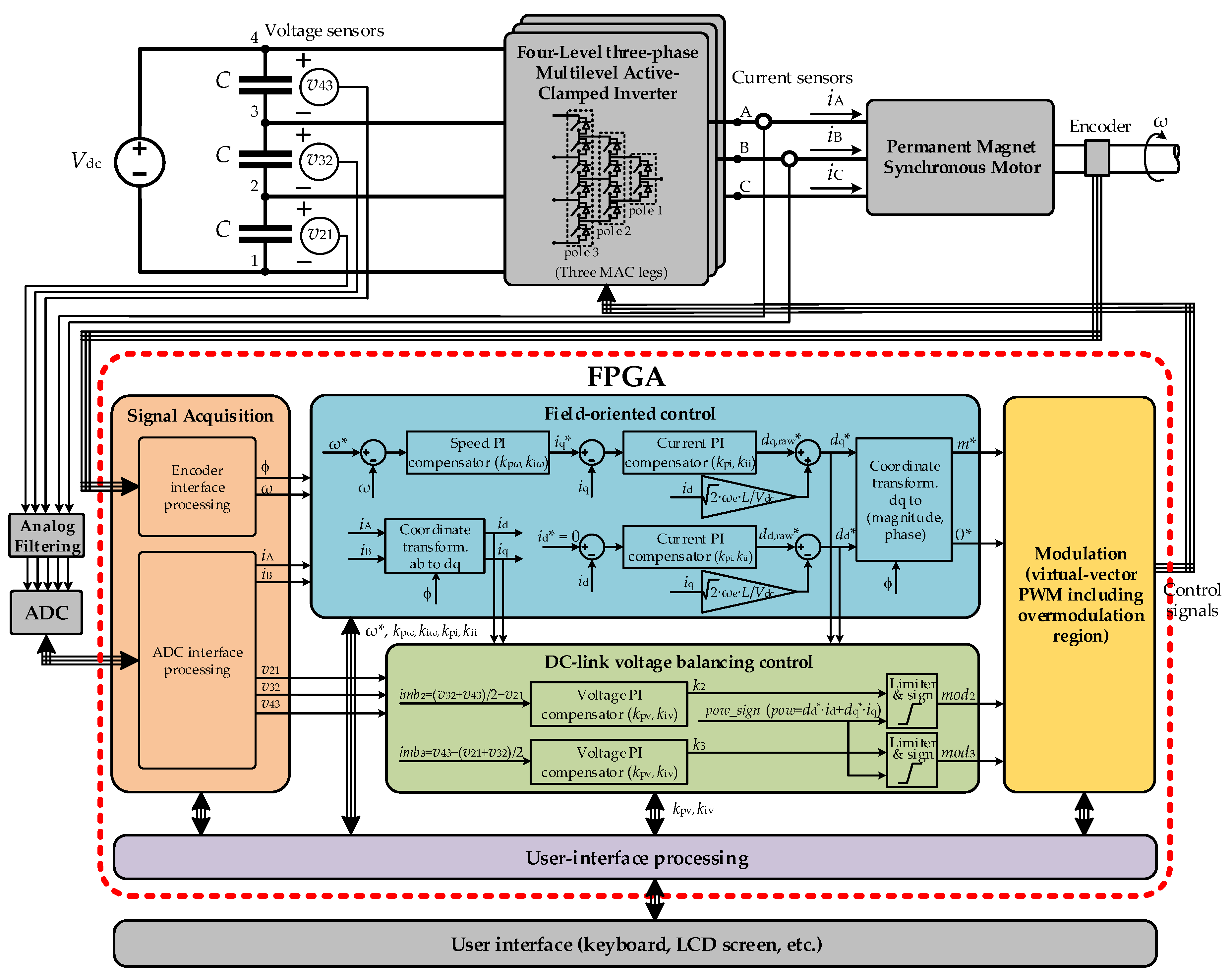
Figure 2 presents the general overview of the electrical circuit and the proposed FPGA control structure. As it can be seen in the
Figure 2, as well as the VBC closed-loop control already introduced above, a closed-loop field-oriented control (FOC) is used for driving the PMSM.
A preliminary open-loop FPGA controller implementation with the same virtual-vector modulation was presented in [
10]. However, the controller in [
10] did not include the closed-loop controls to operate the converter as a motor drive and to preserve the capacitor voltages balanced.
FPGAs have been employed for implementing diverse control schemes of multilevel converters ([
11,
12,
13,
14,
15,
16,
17,
18,
19,
20,
21]), and also for implementing motor-drive controllers ([
17,
18,
19,
20,
21,
22,
23,
24,
25,
26]). References [
17,
18,
19,
20,
21] propose FPGA-based controllers for multilevel converters operating as motor drives, as it is proposed here. However, [
17,
18,
19,
20,
21] do not explain the FPGA controller structure, do not discuss the design methodology to obtain an efficient implementation, and generally do not deal with the voltage balancing problem.
To the best of the authors’ knowledge, for the first time, a complete controller for a four-level converter of the NPC converter family [
4], operating as a motor drive and including DC-link voltage balancing control, is fully-embedded into an FPGA. In addition, the controller implementation has been optimized to save FPGA resources and also to take full advantage of the FPGA potential performance capabilities.
The paper is organized as follows:
Section 2 presents a summary of the used VBC, field-oriented control (FOC), and modulation scheme, presenting the equations to be implemented in the FPGA.
Section 3 details the FPGA structure, and describes relevant aspects to achieve an efficient controller. In
Section 4, experimental results are shown to verify the good operation of the controller under different conditions. Finally,
Section 5 outlines the conclusion.
3. FPGA Design and Control Implementation
Modulation and control structures presented in the previous Section have been implemented on an Altera Cyclone IV EP4CE22F17C6N FPGA device driven by a 50-MHz system clock (Altera, Intel, San Jose, CA, USA). The FPGA application has been described in VHDL.
Figure 3 presents a block diagram of the FPGA application, together with its peripherals. In this figure, six different subsystems are separated in a set of six color boxes, following the same color selection as in
Figure 2. Input signals are located on the left side of the boxes, while output signals are located on the right side. This criterion does not apply to the signals exchanged between the FPGA and peripherals, in which an arrow indicates the direction. For simplicity, only the main variables and constants are shown.
The FPGA has been mounted on a printed circuit board together with the sensors, the filtering circuitry, the ADC chip, and the user-interface (see
Figure 3). The user-interface comprises a 4 × 3 matrix keyboard to introduce the values of some control variables, a three-line sixteen-character LCD screen, two pushbuttons, and eleven LEDs to easily visualize some errors and the ON-state.
Three operating modes have been defined in order to enable the use of the inverter under different system configurations, and also to bring the possibility of evaluating and tuning the different control structures individually:
- -
Voltage-balancing controller mode (mode 0): in this mode, FOC is disabled, but the dc-link voltage control is enabled. With this mode, it is necessary to introduce the command values of m* and f* to make it operate at desired conditions.
- -
Torque controller mode (mode 1): this mode enables the inner current control loop of the FOC, but the outer speed control loop is disabled. DC-link voltage control is also enabled. With this mode, it is necessary to introduce the value of iq*, which is proportional to the torque, to make it operate at desired conditions.
- -
Speed controller mode (mode 2): this mode enables the whole closed-loop control. With this mode, it is necessary to externally introduce the command value of rotational speed ω* to make it operate at desired conditions.
Since the control scheme requires five analog inputs (sensed iA, iB, v21, v32, and v43), and the position of the rotor, an analog-to-digital converter chip and an encoder are necessary.
The AD7658 from Analog Devices has been selected as ADC chip, as it allows converting up to six analog signals synchronously. This chip is configured in parallel interface to minimize the time needed for data transmission.
Encoder RP1410 (IFM, El Prat de Llobregat, Spain) is used for obtaining the rotor position. This encoder generates three digital signals: enc_A, enc_B, and index_zc. Signals enc_A and enc_B present each 1024 pulses for a rotor revolution (with a phase delay of 90°). To determine the rotor angle, any single rising or falling edge of enc_A and enc_B can be counted, giving a resolution of 4096 edges per revolution, so 1024 edges per electrical cycle (the motor is a four-pole PMSM). Then, the mechanical rotor angle φm presents a resolution of 0.08789° (360°/4096 edges), and the electrical angle φ resolution is 0.35156°. Signal index_zc presents a small pulse each time a rotor revolution is accomplished (zero-crossing detection).
3.1. FPGA Basic Design Aspects
A similar design methodology to the one used in [
10] has been also considered here. Variables are represented as integers. For each variable, both units and width (number of bits) have been meticulously selected to obtain the desired resolution and range avoiding underflows/overflows and to reduce FPGA used resources (truncations are often applied). Most of the variables are coded with 12 to 16 bits. Better resolution is not required as sampled variables (i.e., voltages, currents, and rotor position) are acquired just with a 12-bit resolution. Unsigned variables are usually coded in natural binary, while signed variables are coded in two’s complement or sign plus magnitude when required. Divisions by constants (i.e., when changing units or calculating speed) are replaced by products followed by truncations to take advantage of the multipliers integrated in the FPGA. Other divisions are avoided as much as possible. When required, as well as for transcendental functions, they are implemented by ROMs built with the RAM blocks integrated in the FPGA. Symmetries, scaling, and offset addition are applied whenever is possible to minimize the number of bits required to achieve a certain resolution. More details are explained below in the FPGA-module-description subsection.
A 50-MHz system clock clk50M (period
tck = 20 ns) is used to manage the FPGA. Relevant time variables, as delay time
td = 2
tck, blanking time
tb = 40
tck, and switching period
ts = 10,000
tck are defined as multiples of
tck, to optimize FPGA resources. Note that
ts = 200 μs implies
fs = 5 kHz. Note in
Figure 3 the time constants
k_tb,
k_td, and
k_ts, that are defined as
k_tb =
tb/
tck = 2,
k_td =
td/
tck = 40, and
k_ts =
ts/
tck = 10,000.
As in [
10], most of the FPGA processing is synchronized with the switching cycle. A divider-by-10,000 counter
cnt_ts is used to this purpose.
Figure 4 illustrates the timing overview of a
cnt_ts cycle and its synchronization with a switching period. A
cnt_ts cycle starts performing all the samplings and calculations required to stablish the behavior of the next switching cycle, which starts at
cnt_ts = 234, as soon as possible after these calculations are completed at
cnt_ts = 214. The delay between these two events, half a blanking time, is required to properly transit from a switching cycle to the next one (
dx4 can change from a null/non-null value to a new null/non-null value, as explained in [
10]).
A versatile implementation has been conceived, allowing the user to modify important operational parameters through the user interface, such as the operating mode (mode), the PI compensators constants kpω, kiω, kpi, kii, kpv and kiv, or the command values ω*, iq*, m* and f*.
3.2. FPGA Module Description
3.2.1. General Modules
Module MA1 generates periodic enable signals of lower frequencies that are necessary to manage the periodicity of several processes. Enable signals are active high, with a pulse lasting a single tck, which is repeated at the corresponding frequency. For example, enable signal en48k83 (48.83 kHz) is used for handling the writing process of LCD, and enable signal en381H5 (381.5 Hz) is used for the state machine of keyboard inspection and for the state machine of the LCD screen operation. Last output signal count_8_tck is a 3-bit divider, which is used, together with the remaining enable signals, in other processes.
Module MA2 detects an active edge in signal onoff provided by the “ON-OFF” pushbutton, and generates an active high signal edge_onoff, that lasts a single tck. Pushbutton inspection is done at low frequency (23.84 Hz) for filtering possible pushbutton bounces.
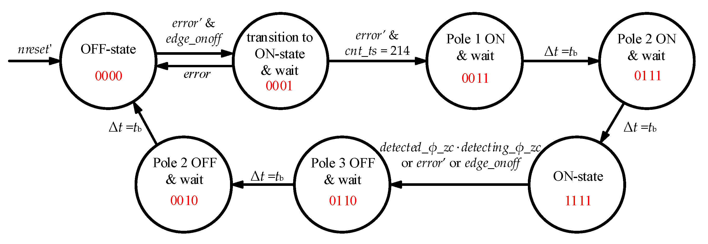
Module M
A3 implements the system ON-OFF finite state machine, which is presented in
Figure 5. Binary values in each state indicate the
system_state output of M
A3. From right to left, bit 0 represents the transition-and-holding bit between OFF and ON states, and bits 1, 2, and 3 represent masking bits for switches in poles 1, 2 and 3, with reference to
Figure 2. In the transition from OFF state to ON state, first pole 1 is enabled, then pole 2, and lastly pole 3. This sequence is reversed in the transition from ON to OFF. When the FPGA is powered on, the motor is driven to rotate at a very low speed in mode 0 (
m* = 0.04 and
f* = 1.22 Hz) to allow an automatic initial zero-crossing detection of the rotor position. Signal
detecting_φ_zc is activated when this automatic detection process is going on. When a filtered first pulse of encoder signal
index_zc is detected, signal
detected_φ_zc is activated permanently (this part of the process is carried out by module M
B1), the motor is stopped, and signal
detecting_φ_zc is deactivated.
Module MA4 generates the global reset signal nreset from the signal rst provided by the “reset” pushbutton. Signal nreset is active low, lasting 120 µs to guarantee minimum duration required by LCD (lcd_nreset and nreset are the same signal). Signal adc_reset, which lasts 10 tck and is active high, is used to initialize the ADC chip.
Module M
A5 is the main synchronization module. It implements the divider-by-10,000 counter
cnt_ts and generates a set of enable signals (
cntts_
X) to manage the timing of most actions performed by other modules, as indicated in
Figure 4. This module also updates the value of line angle in mode 0 (
θ*_
0), from the frequency command value in mode 0 (
f*_0).
3.2.2. Signal-Acquisition Modules
Module M
B1 processes the encoder input signals
enc_A,
enc_B, and
index_zc and generates the angular position
φm of the motor, its angular speed
ω, and the electrical angle
φ. Input signals from the encoder are initially filtered at a sampling frequency of 6.25 MHz (50 MHz/8), discarding any value that has not remained constant for a minimum of eight consecutive samples. The angular position
φm is updated when a new edge in any of the filtered signals derived from
enc_A and
enc_B is detected. A pulse of
index_zc signal should take place every 4096 edges (1 revolution). Non-consistency produces a LED error indication. The angular speed
ω is updated every 2.5 ms, and is calculated dividing the angle rotated in the last 10 ms by this time. The existence of two simultaneous edges in filtered signals derived from
enc_A and
enc_B, as well as an excessive speed, also result in LED error indications. Obviously, this module works asynchronously to the main synchronization module. To synchronize data,
φ and
ω are copied at
cnt_ts = 191 to have convenient values for FOC and VBC processing (see
Figure 4).
Module M
B2 is in charge of handling the ADC chip according to
Figure 4. Signals
adc_start,
adc_ncs and
adc_nrd are generated in the FPGA to control the ADC chip. FPGA receives the acquired data through the 12-bit bus
adc_data. Current
ic is determined from the measured ones (
ic = −
ia −
ib). Values out of acceptable range result in LED error indications.
3.2.3. User-Interface Modules
Module MC1 comprises two finite state machines that handle the 4 × 3 matrix keyboard operation. A first finite state machine handles the detection and identification of the keyboard buttons when any of them is pressed. A second finite state machine identifies the sequence of the different buttons pressed in order to determine the actions to be executed: acquisition of the identifier of the parameter to be shown in the LCD screen, modification of the value of a configurable parameter, etc.
Module M
C2 implements three concurrent finite state machines that manage the configuration and visualization of the LCD screen. The LCD screen shows the name of the variable selected by the user to be visualized, with its current value, its identifier number and its allowed range (just for the configurable parameters). The module also includes a ROM containing the visualization format for the 24 variables that can be visualized in the LCD screen (see
Figure 3).
The user-interface modules consume substantial resources of the FPGA (21.5% of the used logic elements and 27% of the used multipliers). Its explanation is simplified here because they are considered to be of less technical importance, compared to other parts of the design.
3.2.4. FOC Modules
Module MD1 simply generates a limiting speed ramp whenever the speed command changes. Module MD2 consists of the speed-error PI compensator with limited proportional, integral and total outputs. Its output value is the quadrature current command value in mode 2 (iq*_2), which is updated when cnt_ts = 192. In mode 1, the quadrature current command value (iq*_1) is set externally. Module MD3 is a selector of iq* depending on the chosen operating mode.
Modules M
D4, M
D5, and M
D6 are in charge of implementing the coordinate transformation. Module M
D4 implements simple logic to calculate angle
φ + 60°. Module M
D5 implements a dual-port ROM that allows obtaining the following four trigonometrical functions in a single
tck, which are necessary to determine the values of
id and
iq:
Module MD6 implements Equation (1) to calculate the values of id and iq. Module MD7 contains the id and iq error PI compensators with limited proportional, integral and total outputs. Output variables of PI compensators are direct and quadrature raw duties dd,raw* and dq,raw*, which are updated when cnt_ts = 194.
Module M
D8 implements the calculation of the decoupling factor, which is equal to
(where
L and
Vdc are usually constant values), its products by currents
id and
iq, the addition of the first product to
dq,raw* and the subtraction of the second product from
dd,raw*, to obtain duties
dd* and
dq*, respectively (see
Figure 2). In general, products are done followed by a truncation (change of units), thus allowing optimizing FPGA resources.
Modules MD9 and MD10 implement the dq-to-(magnitude,phase) transformation indicated in Equation (2) to calculate the modulation index and reference vector angle in modes 1 and 2 (m*_12 and θ*_12). Both variables are obtained through a successive approximation algorithm. A ROM is used to calculate the tangent of the provisional reference vector angle used in the algorithm. Octagonal symmetry is taken into account to reduce the size of the ROM.
Module MD11 is just a selector for the modulation index and the reference vector angle, depending on the operating mode.
3.2.5. VBC Modules
Module ME1 calculates the voltage imbalances at dc-link points 2 and 3 (imb2 and imb3) and includes the PI compensators for the error of these variables, also calculated in the module.
Module M
E2 consists of a ROM delivering the following auxiliary functions, which are necessary to determine the values of
and
, as shown in
Table 1:
Module M
E3 is in charge of calculating the sign of power flow, according to the expression shown in the green inset of
Figure 2. Output value of
pow_
sign is updated at
cnt_ts = 196.
Module M
E4 applies simple logic to obtain values of variables
and
, according to
Table 1.
3.2.6. Modulation Modules
Module M
F1 adapts the value of the reference vector angle to be an angle within the first sextant ([0°, 60°[). The sextant values corresponding to the three phases are also determined, and given through the variables
sextant_x. Module M
F2 modifies
θ and
m*, according to
Table 2 and
Table 3. A ROM is used to calculate the function
m = 0.98/sin (
θ + 60°). Module M
F3 calculates the values of
d1,
d4 and
d5, according to Equation (4). Two ROMs are used to calculate
d1 and
d4.
Module M
F4 includes a ROM for calculating the value of
kmod, according to Equation (6). The ROM address, which is defined as the result of expression 3 +
–
, is previously calculated through module M
F5. Module M
F6 calculates the following products, which are useful to calculate modified duty ratios
,
,
, and
:
Module M
F7 (one per phase) calculates
,
,
, and
according to Equation (6) and
Table 4, and transforms them into time variables
tx1,
tx2,
tx3 and
tx4 as multiples of
tck. Modules M
F8 and M
F9 (one per phase) are the same used in [
10].
3.3. Consumed FPGA Resources
The resources used to synthesize the whole design using the Quartus II software are shown in
Table 5. The complete FPGA implementation has been done making a substantial effort to save FPGA resources. As it can be seen, enough FPGA resources are still available. They can be used, for example, to include additional features in the design, to increase the switching frequency, and/or to improve the variables resolution. Furthermore, it is relevant to recall that, for practical applications, the user-interface processing is usually not required, which would increase even more the remaining FPGA resources.
3.4. Control Processing Time
In order to minimize the processing time for obtaining the next-switching-cycle duties and therefore maximize the closed-loop control bandwidth, an ad hoc processing unit has been fully embedded within the FPGA, instead of using a general-purpose processor. The resulting processing time, taken from the command to sample and convert the analog signals delivered by the sensors (
cnt_ts = 0), until the instant when all the duties needed to generate the following switching cycle become available (
cnt_ts = 214), is 4.28 µs (see
Figure 4). Thus, the switching frequency could be increased until approximately 1/5 µs = 200 kHz. To maximize the control bandwidth, the processing occurs as close as possible to the start of a new switching cycle.
4. Experimental Tests
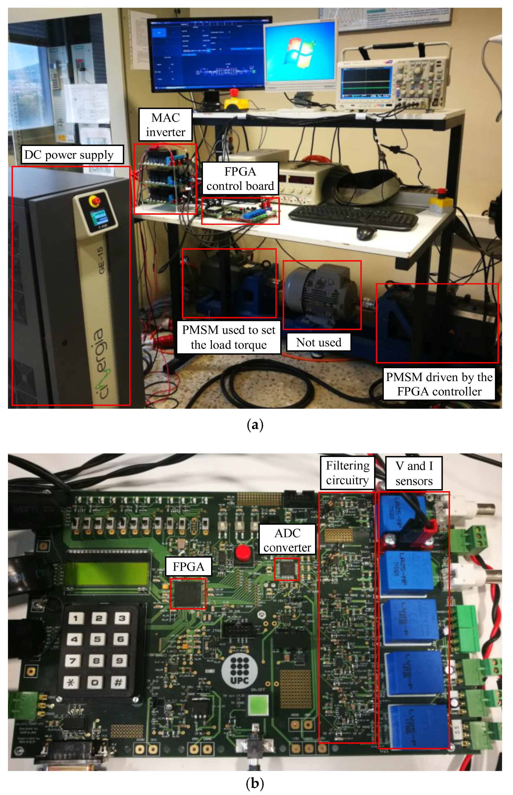
The proper operation of the FPGA controller has been tested experimentally within the system shown in
Figure 6a. Main parts of the system are labelled in the figure. The shaft of the PMSM driven by the FPGA controller is coupled to an induction machine, which is not used, and also to another PMSM, which is used to set the load torque. A further detailed overview of the experimental test bed can be observed in a
supplementary video attached with this paper.
Figure 6b depicts FPGA control board, presenting its main parts/subcircuits.
The four-level three-phase MAC inverter employs 200 V STP20NF20 MOSFET devices (ST microelectronics, Amsterdam, Netherlands). The reference of the PMSM driven by the FPGA controller is 1FT6105-8SB71-2AA0 (Siemens, Berlin, Germany). This motor is a surface-magnet type PMSM, with a nominal speed of 1500 rpm and a nominal torque of 59 Nm, thus, a nominal power of 9.27 kW.
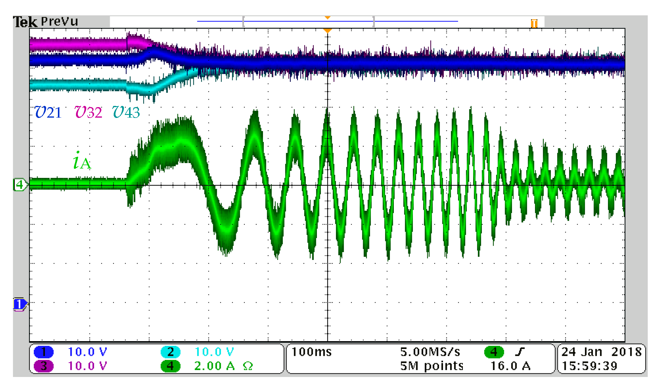
The proper system operation can be observed in
Figure 7,
Figure 8 and
Figure 9. In
Figure 7, the good performance of the VBC under a start-up transition is depicted. Initially, in OFF state, capacitor voltages are unbalanced, but after 200 ms of operation, they become balanced. It is also remarkable the behavior of the phase current
iA. After the start-up, while the motor is accelerating, the current magnitude keeps constant at a certain level, set by the speed ramp. As soon as the motor reaches the command speed of 500 rpm, the current magnitude decreases to a lower level.
Figure 8 shows the phase currents under a change of rotation direction, from 350 rpm to −350 rpm. In the upper part of the figure, the whole transition is depicted. As it can be seen, the current sequence changes once the motor starts rotating in opposite direction. As in
Figure 7, once the motor reaches the command speed value, the current magnitude decreases to a lower level.
Figure 9 presents the three phase currents and the phase voltage
vA1 operating in UM and OM regions.
Figure 9a shows the waveforms for the UM region, with
m* = 0.76.
Figure 9b shows the waveforms for region OMI (0.98 <
m* < 1.028), operating with
m* = 1.01.
Figure 9c shows the waveforms for region OMII (1.028 <
m* < 1.081), operating with
m* = 1.03. In UM, current waveforms are sinusoidal with almost no distortion. However, in OMI and OMII, the current waveforms present a noteworthy distortion, with a higher distortion under OMII. This is the expected behavior, since the overmodulation intrinsically introduces low-order harmonics in the phase currents [
27]. It is also interesting to note that in waveforms of the phase voltage
vA1, the duty ratio of connection to inner levels 2 and 3 is lower when operating in OM region.
As stated previously, a complementary video is included with this study. The video shows the whole system operating under conditions of
Figure 7 and
Figure 8, and also under other different conditions.

 ,
, 


