An Improved Autonomous Current-Fed Push-Pull Parallel-Resonant Inverter for Inductive Power Transfer System


1
School of Microelectronics and Communication Engineering, Chongqing University, 174 Shazheng Street, Shapingba District, Chongqing 400044, China
2
Chongqing Engineering Laboratory of High Performance Integrated Circuits, Chongqing 400044, China
*
Author to whom correspondence should be addressed.
Energies 2018, 11(10), 2653; https://doi.org/10.3390/en11102653
Submission received: 8 August 2018
/
Revised: 23 September 2018
/
Accepted: 1 October 2018
/
Published: 4 October 2018
(This article belongs to the Special Issue Wireless Power Transfer 2018)
Abstract
:In the inductive power transfer (IPT) system, it is recommended to drive the resonant inverter in zero-voltage switching (ZVS) or zero-current switching (ZCS) operation to reduce switching losses, especially in dynamic applications with variable couplings. This paper proposes an improved autonomous current-fed push-pull parallel-resonant inverter, which not only realizes the ZVS operation by tracking the zero phase angle (ZPA) frequency, but also improves the output power and overall efficiency in a wide range by reducing gate losses and switching losses. The ZPA frequencies characteristic of the parallel-parallel resonant circuit in both bifurcation and bifurcation-free regions is derived and verified by theory and experiments, and the comparative experimental results demonstrate that the improved inverter can significantly increase the output power from 7.68 W to 8.74 W and has an overall efficiency ranging from 63.5% to 72.5% compared with the traditional inverter at a 2 cm coil distance. Furthermore, with a 2-fold input voltage (24 V), the improved inverter can achieve an approximate 4-fold output power of 38.9 W and overall efficiency of 83.6% at a 2 cm coil distance.
1. Introduction
Inductive power transfer (IPT) technology [1], characterized by convenience and safety, has many potential applications in portable devices [2], wireless sensor networks (WSNs) [3], implant medical devices (IMDs) [4,5,6,7], and electrical vehicles [8,9,10]. In general, it is recommended to drive the primary-side inverter of IPT systems at zero phase angle (ZPA) operation in order to minimize the volt-amp (VA) rating of the source supply. Moreover, the resonant inverter can achieve zero-voltage switching (ZVS) or zero-current switching (ZCS) operation with less switching losses and electromagnetic interference (EMI) at ZPA or a similar condition [11,12,13]. However, it is often a great challenge to maintain ZVS or ZCS operation with variable couplings, caused by nonconstant coil distances, misalignment, shape deformation, or metal object proximity. Especially when it occurs to the frequency bifurcation region, the power transfer capability and efficiency can deteriorate rapidly at the original resonant frequency [2,13].
Various solutions have been proposed in the previous literature. One is dynamic tuning of reactive elements in either the primary or the secondary compensation network through variable inductors [14,15,16], switchable capacitor bank [9], or transistor-controlled variable capacitor [17], respectively. This method aims to keep the ZVS frequency fixed under coupling variation, although it needs more switching devices, passive components, and even a complicated control unit. Moreover, another common method is directly adjusting the inverter frequency to the new ZVS frequency as the magnetic coupling changes. For instance, in [18], the authors present a closed-loop automatic frequency tuning system by an optimum frequency tracking method in an overcoupled regime with the aid of an extra control unit. Similarly, in [19], an automatic adaptive frequency tracking system was implemented on the basis of feedback power efficiency via 2.45 GHz data transmission. The drawbacks of these systems are the cost and time delay due to the existence of communication and control units. To achieve a cost-effective small-for-size IPT system, an autonomous current-fed push-pull inverter used in a parallel-resonant circuit structure was proposed in [20,21], and this system has the ability to naturally track the ZPA frequency of a parallel-parallel resonant network without any extra control or communication units. What is more, the two active power switches in the inverter are common ground, and consequently, the gate drive structure is rather simple with no need for a high-side gate drive. With these advantages, this inverter structure is a potential choice for dynamic applications, but the gate drive problem is often neglected in practice, especially in low-power applications. The authors in [22] proposed and analyzed this issue, then they modified the inverter by adding speedup capacitors in the gate drive circuit, which reduced the gate losses and extended the switching frequency range into the MHz region. However, the value of speedup capacitors should be calculated and selected carefully in advance based on the predefined drive resistances and operating frequency, which means it is not suitable in dynamic applications.
This paper presents an improved current-fed push-pull parallel-resonant inverter with a powerful gate drive circuit and flexible input source configuration for dynamic applications. Compared with the traditional inverter, it enhances the gate drive capability and thus reduces the gate losses as well as the switching losses in a wide range. Furthermore, the maximum power transfer limitation is removed, and the system’s overall efficiency increases due to the input voltage adjustment. First, the impedance characteristic of a parallel-parallel resonant circuit was analyzed theoretically and the exact and approximate solutions of ZPA frequencies in both bifurcation and bifurcation-free regions were derived. Then, the gate drive losses and switching losses were analyzed and simulated, and the corresponding improvements are presented. Last, an improved inverter prototype is proposed, and the results are compared and analyzed with those of a traditional inverter.
2. Operating Principle of Autonomous Current-Fed Push-Pull Circuit
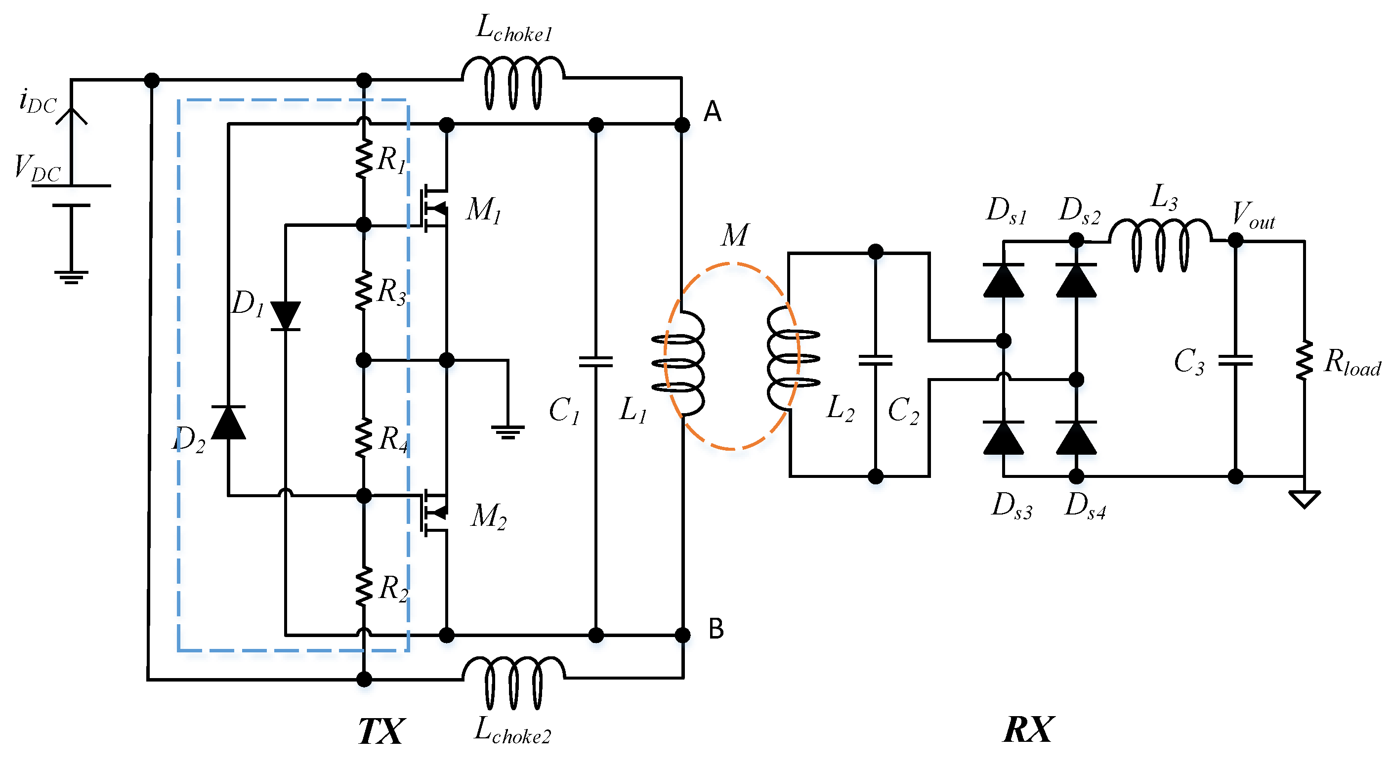
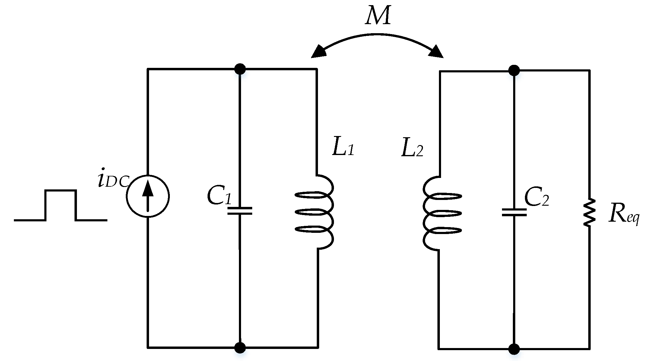
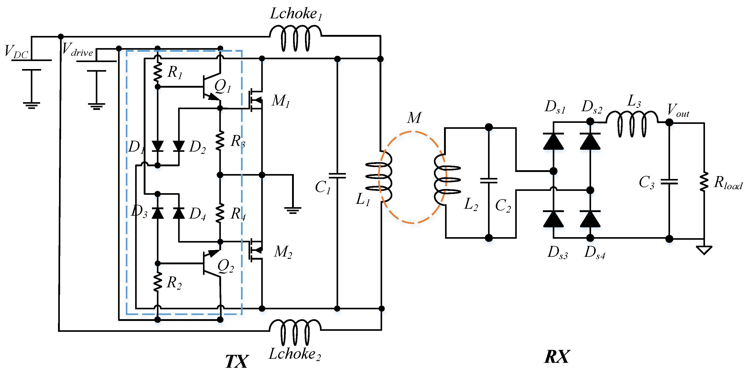
A traditional autonomous current-fed push-pull IPT system, including transmitter and receiver, is presented in Figure 1 [20,21]. Compared with the resonant inductors ( and ), two relatively large inductive chokes ( and ) are connected serially with the DC input voltage source and form a quasi-current source. Under a steady-state condition, the two inductive chokes divide the DC current into two halves and feed the current into the primary LC tank ( and ) alternately. Therefore, the current injected into the primary LC tank is an approximate square waveform with half the magnitude of the DC current. Then, AC power is transferred from the primary resonant LC tank to the secondary side ( and ) by magnetically coupling, and then provided to the terminal DC load after the rectifier bridge (–) and LC filter and . According to [23], the rectifier, LC filter, and DC load can be replaced by an AC equivalent resistance , and the equivalent circuit of current-fed push-pull parallel-resonant circuit can be simplified, as shown in Figure 2.
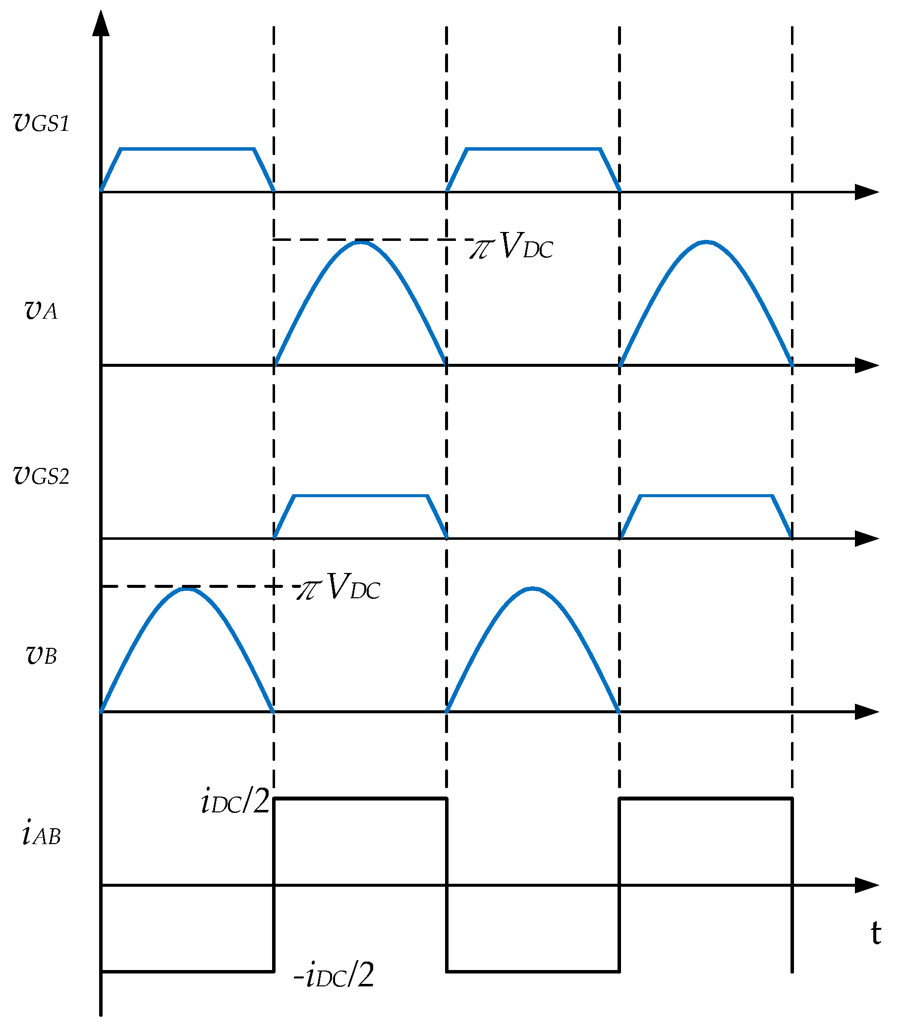
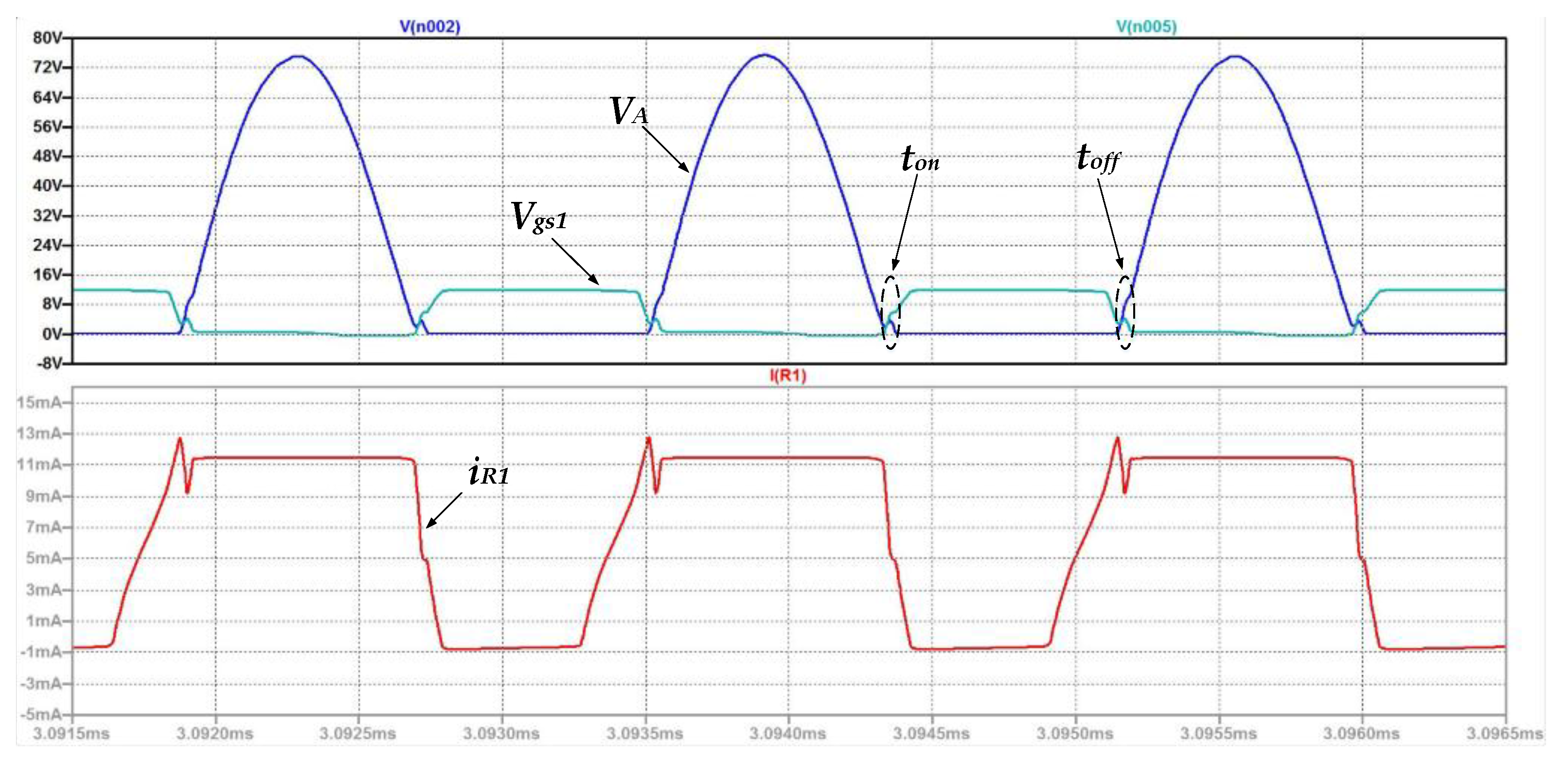
One assumption of the equivalent circuit in Figure 2 is that the two MOSFETs (metal oxide silicon field effect transistors) are always driven at the resonant frequency of the magnetically coupled primary LC tank, and this is achieved by the gate drive circuit of the two MOSFETs going into the blue dashed line in Figure 1. The gates of the two MOSFETs ( and ) are connected with two large pull-down resistors ( and ) to ground and two current limiting resistors ( and ) to the DC voltage source. In addition, two cross-connected diodes ( and ) take the resonant voltage signal at the drain of one MOSFET to the gate of the other MOSFET like a bistable multivibrator. When the inverter is powered on, one of the two power MOSFETs will turn on first due to their parameter differences, noise, and disturbances, which makes the current inject into the LC tank and the TX tank begin to oscillate. At steady state, when one power MOSFET, such as , turns on, the drain voltage is almost zero to ground, which clamps the gate voltage of at just a forward diode drop above zero by and thus keeps in the off state. Meanwhile, the voltage at terminal-A of is fixed at the gate voltage of , which is approximately the DC voltage (), and the voltage at terminal-K of is equal to the resonant sinusoidal voltage at the drain of . So, the diode is reverse biased until the resonant voltage falls below the DC voltage. A similar procedure occurs for the other side of the LC tank, but in the opposite direction, in the second half-cycle. The waveforms of corresponding voltages and currents in one switching cycle are shown in Figure 3.
According to the volt-second balance of an inductor at steady state, the average voltages across the inductive chokes are zero and the following relationship can be obtained as [23]:
where and are the magnitude of resonant sinusoidal voltage.
3. ZPA Frequency Analysis of Parallel-Resonant Circuit
In order to keep the inverter at ZVS operation with varying coupling coefficients, it is necessary to analyze the impedance characteristic of the parallel-parallel resonant circuit.
Due to the bandpass filter characteristic of a parallel-resonant circuit, all the other harmonics are filtered out except for the fundamental component, so the rectangular wave current source in Figure 2 can be replaced by its fundamental component-sinusoidal current source after ignoring the higher harmonics, and the relationship is
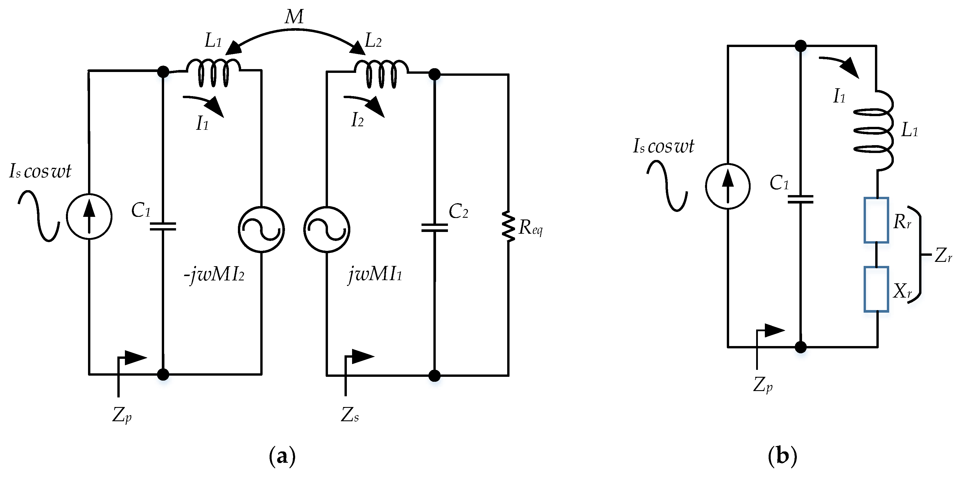
With the sinusoidal current source and the mutual inductance coupling transformer model, the equivalent circuit can be simplified, as in Figure 4a. It can be seen that the load impedance of the secondary side is expressed as
Additionally, the reflected impedance from the secondary to primary side , which is in series with primary inductor L1, can be obtained as
where and represent the reflected resistance and reactance, respectively. is the mutual inductance. Thus, the circuit can be further simplified, as in Figure 4b.
The input impedance of the resonant LC tank in Figure 4b can be written as
Substituting Equations (3) and (4) into (5) and the mutual inductance , where k is the coupling coefficient, the input impedance can be expressed as
Here, we get the ZPA frequency points of the input impedance by equating its imaginary component to zero,
and with Mathmatica software, it can be expanded as
On the assumption that both sides of the network have the same free resonant angular frequency , the complex form of Equation (8) can be simplified as
where is defined as the normalized frequency and is the quality factor . Furthermore, the symbols A and B are denoted as
It is obvious that the solutions of Equation (9) depend on two equations (ignoring the solution ): the trough equation and ridge equation [24].
1. The Trough Equation
The discriminant of the trough equation is nonnegative, so there are two roots of the equation with opposite signs. After excluding the impractical negative root, we take the positive root as the trough point, which is the middle bifurcation frequency
2. The Ridge Equation
The ridge equation is a biquadratic equation, which can be treated as a quadratic equation with , and it can be simplified as
In the bifurcation region, (12) has two positive roots. According to the Descartes’ sign rule and the nonnegative discriminant principle, we get the following preconditions:
where is denoted as the critical bifurcation coupling coefficient, representing the key point between the bifurcation region and the bifurcation-free region. In the meantime, the bifurcation frequency at the critical bifurcation coupling point is . Because holds, can always satisfy Equation (13). Under the preconditions of (13) and (14), the roots of Equation (12) are
and when holds, (15) can also be simplified as
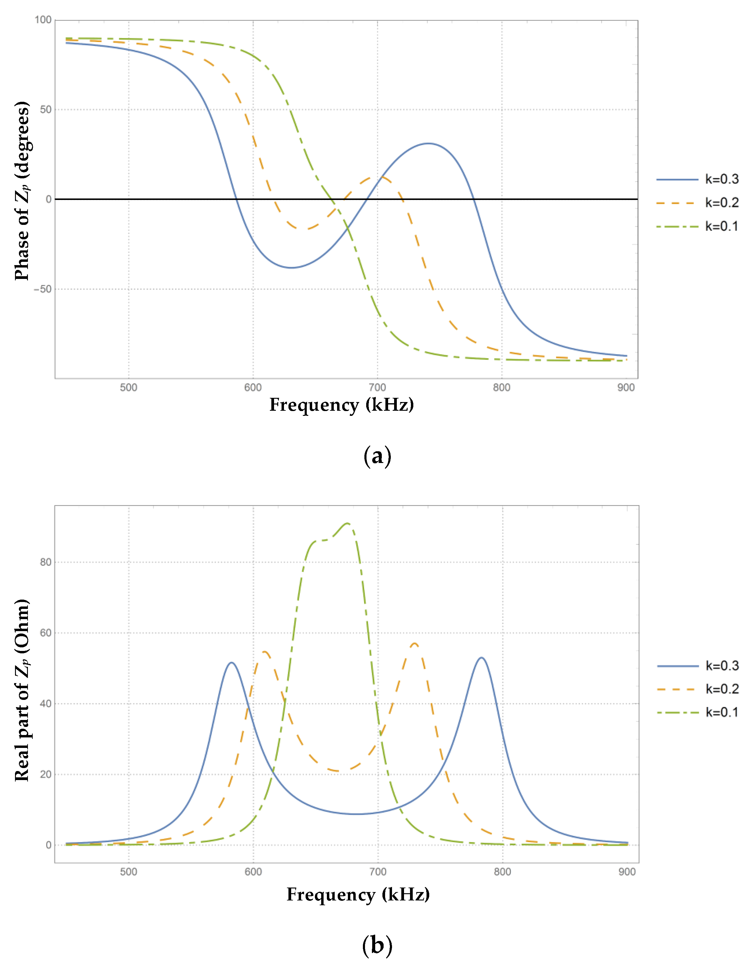
The two ZPA frequencies derived from the ridge equation (the small bifurcation frequency and the great bifurcation frequency ) sit on both sides of the free resonant angular frequency or the middle bifurcation frequency , and their relationship is . For intuitive understanding, three numerical simulations were performed with different coupling coefficients (k = 0.1, 0.2, and 0.3), and the parameters are: uH, nF, Ω. The results of the phase angle and real part of are plotted in Figure 5.
According to Equation (14), the bifurcation coupling coefficient kb is about 0.1312 and the free resonant frequency f0 is 660 kHz for this system. As illustrated in Figure 5a, there exist three ZPA frequencies in the bifurcation region (i.e., k = 0.3 or k = 0.2). The middle bifurcation frequency is near the free resonant frequency f0, while the other two ZPA frequencies are distributed at both sides of the middle bifurcation frequency fm. Furthermore, the deviation between the middle bifurcation frequency fm and the free resonant frequency f0 become larger as the coupling coefficient increases, as does the distance between the other two ZPA frequencies. In the bifurcation-free region (i.e., k = 0.1), there is only one ZPA frequency fm near the free resonant frequency f0.
Figure 5b illustrates the real part of input impedance Zp for different coupling conditions. It is obvious that two impedance peaks appear at the two-side ZPA frequencies f+, f− and one impedance trough at the middle bifurcation frequency fm in the bifurcation region (i.e., k = 0.3 or k = 0.2). According to [6], the output power of the inverter is proportional to the input DC voltage, and the relationship is
where is the real part of . The two impedance peaks at both sides are close to each other and can get the approximate output power at the two ZPA frequencies, while more power can be obtained at the middle bifurcation frequency under the same coupling condition due to the low input impedance. However, the ZVS operation to the middle bifurcation frequency is unstable without an external complex controller [25]. When in the bifurcation-free region (i.e., k = 0.1), there exists only one ZPA frequency near the input impedance peak. The simulation results imply that the inverter should track the small or great bifurcation frequency in the bifurcation region and the middle bifurcation frequency in bifurcation-free region to maintain ZVS operation against coupling variation.
4. Analysis of Gate Drive Circuit and Proposed Inverter
4.1. Gate Circuit Analysis
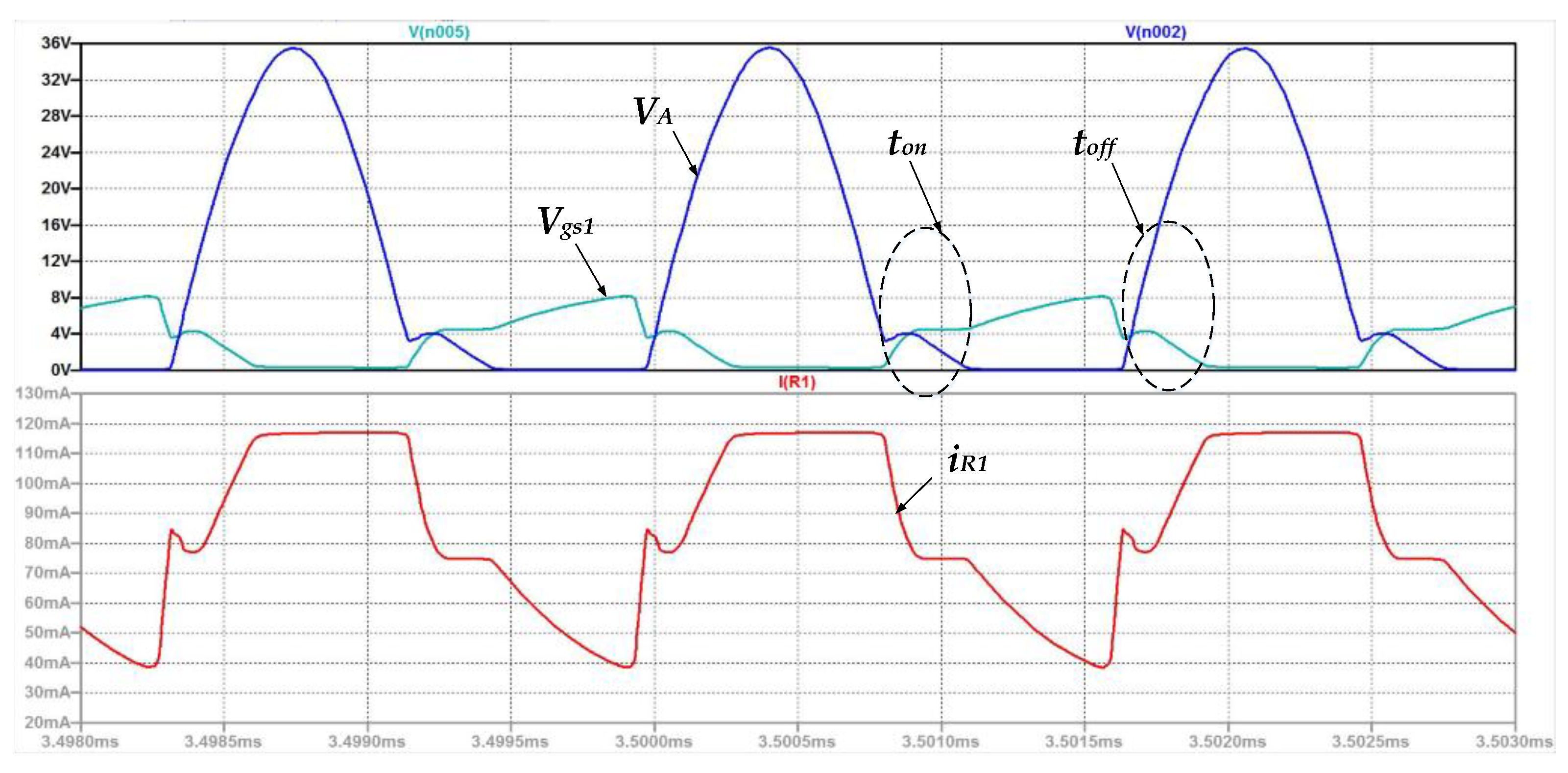
According to the analysis in Section 2, the traditional autonomous current-fed push-pull inverter in Figure 1 can track the ZPA frequency of a parallel-resonant circuit automatically by the feedback zero-crossing resonant voltage signals from the LC tank. In practice, the selection of the current limiting resistance and is a dilemma between gate drive losses and switching losses. To explain this, a SPICE simulation using the circuit parameters and components listed in Table 1 and Table 2 at 12 V DC input was carried out in LTspice XVII under the coupling coefficient , and the waveforms of the gate voltage and current are shown in Figure 6.
For one thing, when one of the MOSFETs turns on—say is on and is off—the clamp diode connected with the drain of forms a current leakage path with resistance , and so does the diode with resistance in the next half-cycle. The lower part of Figure 6 shows that the current flowing through is about 116 mA when turns off and the power loss on the two current-limiting resistances is about 1.3 W. In order to reduce this gate loss, a high value of and is preferred.
For another thing, the current limiting resistance or with the input parasitic capacitor of or constitutes a first-order RC circuit, which turns on the MOSFET by charging the input capacitor. The time constant determines the charging speed and seriously affects the switching losses of the MOSFETs. As shown in the upper part of Figure 6, the gate voltage rises slowly to approximately 8 V on account of the limited charging current. The turn-on switching delay and turn-off switching delay of the MOSFETs at a 603 kHz switching frequency are 279 ns and 297 ns, respectively, which may cause severe switching losses. In order to improve the signal quality and reduce switching losses, lower resistances and are needed. Therefore, in the traditional inverter structure, the contradiction between gate drive losses and switching losses cannot be solved at the same time.
4.2. Improved Inverter
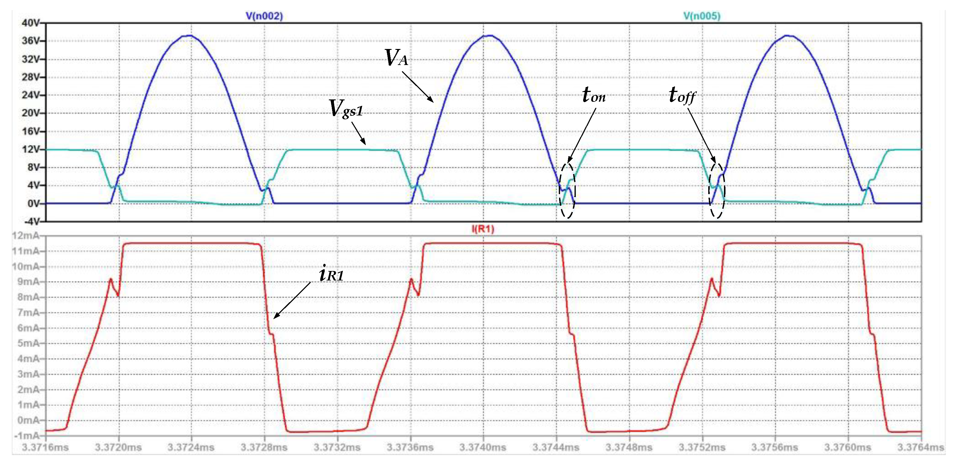
An improved autonomous current-fed push-pull inverter is proposed in Figure 7. Two BJT (bipolar junction transistor) switches and with base resistances and supply the charging current to the gates of MOSFETs and alternatively, and they replace the current limiting resistances in the traditional design with zero voltage detection control by two cross-connected diodes and . Additionally, the other two cross-connected diodes and perform the same function for the MOSFETs as in the traditional design. One advantage of the improvements is that with the characteristic of high current transfer ratio , low saturation voltage , and low saturation resistance , the transistors and pull a high charging current to the gates of the MOSFETs, which speeds up the turn-on procedure of the MOSFET and maintains the gate voltage close to the drive source voltage. Meanwhile, it is possible to apply a high value of and to decrease the leakage current due to the low base current of transistors. A relevant simulation was carried out using the parameters and components listed in Table 2 and Table 3 at V and V under the same coupling condition. Corresponding waveforms are presented in Figure 8, and it is obvious that the waveform of gate voltage is improved and the voltage is maintained at a 12 V drive source voltage when turns on. The turn-on switching delay and turn-off switching delay of MOSFETs at a 608 kHz switching frequency are 67 ns and 72 ns, respectively, which are obviously shorter than those in Figure 6. In addition, the leakage current of is down to 12 mA and the gate loss is close to 1/10 of that in traditional circuit simulation.
Another advantage of the proposed inverter is the separation between the DC voltage source and drive voltage source . In the traditional inverter, the value of the DC voltage source is often restricted to a certain range below the maximum gate voltage of the MOSFET, avoiding device damage. However, this hinders the possibility of increasing the transmission power regarding Equation (17). The separation of voltage sources removes this transmission power restriction by increasing the DC voltage source and maintaining the gate voltage constant simultaneously, which makes the design more flexible in practice. A simulation with the same parameters as those in Table 2 and Table 3 was carried out at V and V under the same coupling condition. In Figure 9, the magnitude of is increased to about 76 V, while the gate voltage and the leakage current remain the same as in Figure 8. The turn-on switching delay and turn-off switching delay of MOSFETs at a 611 kHz switching frequency are 44 ns and 56 ns, respectively, which are shorter than those in Figure 8 due to the decrease of input capacitor caused by higher (i.e., ).
5. Experimental Verification
5.1. Experimental Setup
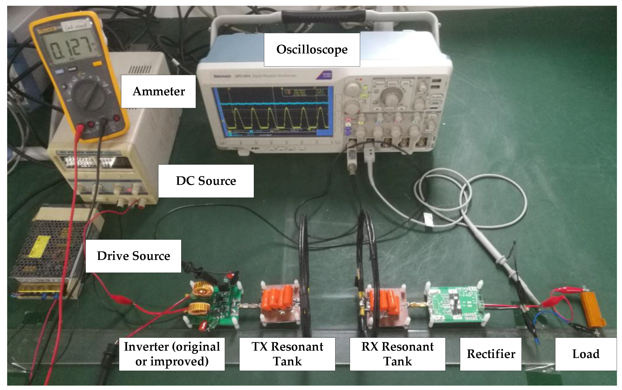
To verify the simulation results and the performance of the proposed inverter, a prototype system with two different inverters was implemented and is shown in Figure 10.
In the experimental setup, the TX and RX coils were separated along their common axis with a distance from 2 cm to 20 cm in steps of 2 cm, and their parameters were the same as those in Table 2. For the sake of performance comparison, two inverters (traditional version and improved version) were manufactured according to the parameters listed in Table 1 and Table 3. An oscilloscope (Tektronix: DPO3054) was used to record the voltage waveforms of the two MOSFETs and measure the load voltage magnitude simultaneously. A 12 V switching power was adopted as the drive source, whose current was measured by an ammeter (Fluke: 15B+), and the DC source was implemented using an adjustable voltage source with a current recording function. Three experiments were performed at different conditions: Experiment 1 (Exp 1) with a traditional inverter at V, Experiment 2 (Exp 2) with the improved inverter at V, and Experiment 3 (Exp 3) with the improved inverter at V and V. To avoid failure at start-up, the voltage of the DC source should be increased slowly during the experiment after turning on the drive source [26].
5.2. ZPA Frequency Bifurcation and Tracking
Before comparing the measured frequency points with the calculated ZPA frequency curves, it is necessary to calculate the relationship between coil distance and coupling coefficient. The mutual inductance between TX and RX coils can be computed by the Neumann formula for multiple turn coils [10,27] as
where is the distance between the incremental lines and , is the permittivity of free space, and , are the turn numbers of the two coils, respectively. Equation (18) can also be expressed as [28]
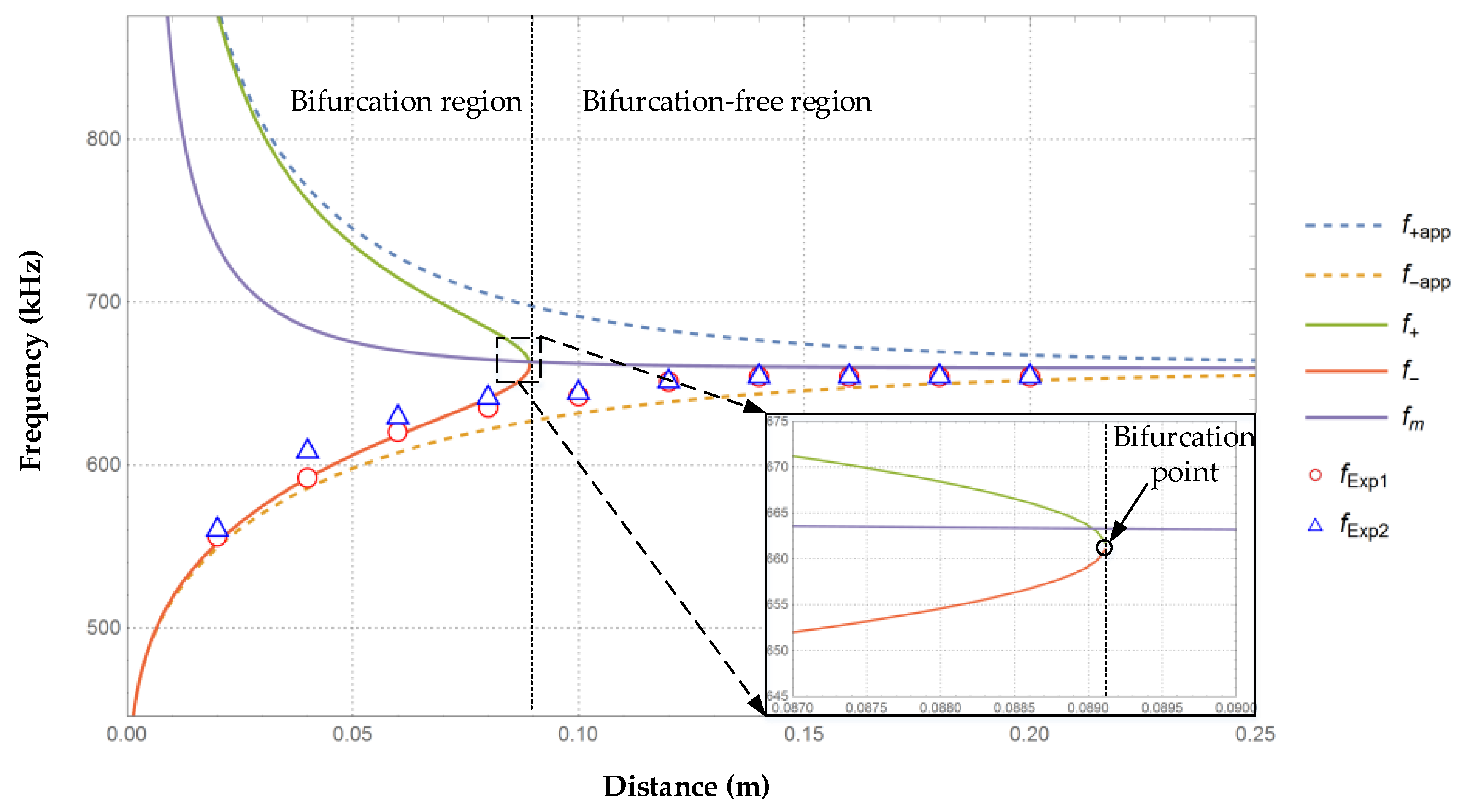
where and are the radii of the coils, and is the distance between the two coils. By substituting Equation (19) into Equations (15) and (16), the theoretical results, as well as the measured data, are plotted in Figure 11.
In Figure 11, the measured frequency data are marked as data points (red circle for Exp 1 data and blue triangle for Exp 2 data ), the theoretical exact solutions in Equations (11) and (15) are plotted as solid lines (green for the great bifurcation frequency , red for the small bifurcation frequency , and purple for the middle bifurcation frequency ) and the approximate solutions of Equation (16) are presented as dashed lines (blue for the great bifurcation approximate frequency and yellow for the small bifurcation approximate frequency ).
The frequency bifurcation phenomenon is obvious in Figure 11, and the great bifurcation frequency and the small bifurcation frequency will merge together at the bifurcation coupling point , i.e., m between the two coils, which is marked in the partial enlarged image. In the left bifurcation region, there always exists more than one ZPA frequency point and the middle bifurcation frequency becomes larger as the separation distance decreases, which is different from the series-series resonant circuit in [24]. The measured frequency data of Exp 1 and Exp 2 are in good agreement with the small bifurcation curve, as well as the small bifurcation approximate frequency curve in the bifurcation region. While in the right bifurcation-free region, the great and small bifurcation frequency disappear and only the middle bifurcation frequency point exists, which approaches the free resonant frequency kHz infinitely, like the two approximate solutions, as separation distance increases. The measured frequency data of Exp 1 and Exp 2 also approach the free resonant frequency with the coils apart in the bifurcation-free region. The slight difference between the measured and calculated results may be from the ignoring of the coils’ parasitic resistances and higher harmonics in the theoretical model. These results demonstrate that the improved inverter can track the ZPA frequency automatically, just as the traditional inverter does, which means the inverter can achieve ZVS operation as the coupling varies.
5.3. Power and Efficiency Comparison
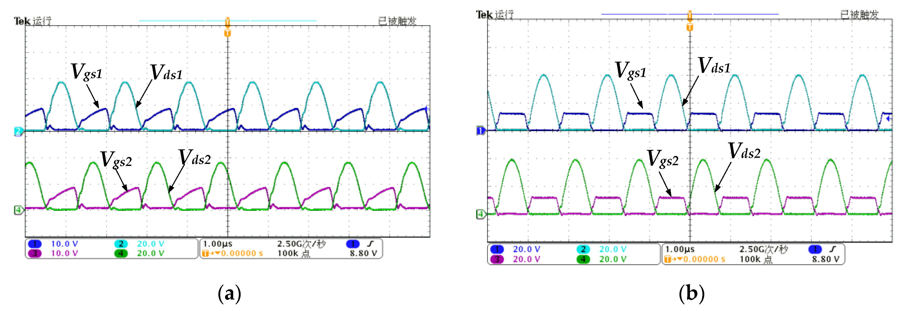
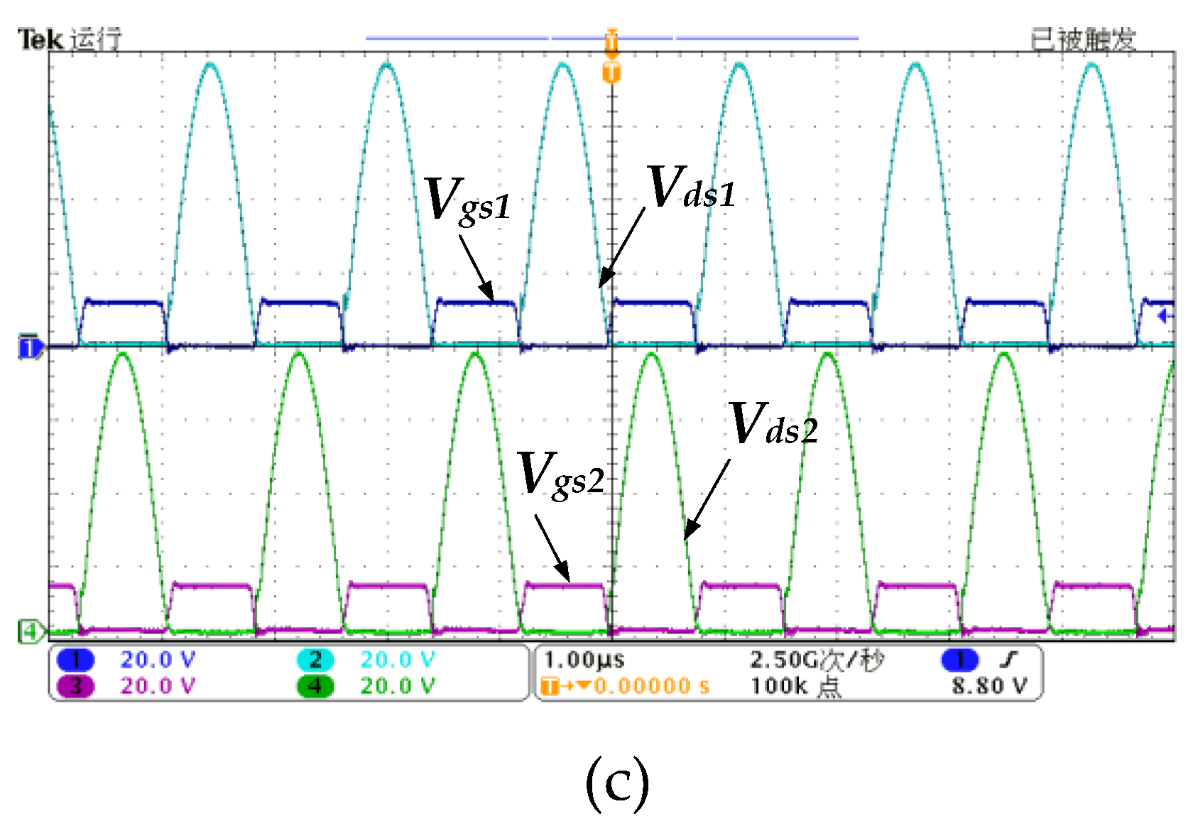
Figure 12a–c show that the practical voltage waveforms are similar to the simulation results in Figure 6, Figure 8, and Figure 9. The gate drive signal of one MOSFET always rises with the resonant voltage at the drain of another MOSFET simultaneously in the three experiments, and the gate drive signal quality has been improved effectively due to the improved gate drive circuit in Exp 2 and Exp 3. The turn-on switching delay and turn-off switching delay of the MOSFETs are 223 ns, 246 ns in Exp 1; 61 ns, 69 ns in Exp 2; and 42 ns, 48 ns in Exp 3. Moreover, the magnitude of the resonant voltage at the TX LC tank in Exp 3 is about 75.2 V, which is consistent with the voltage Equation (1) indicated.
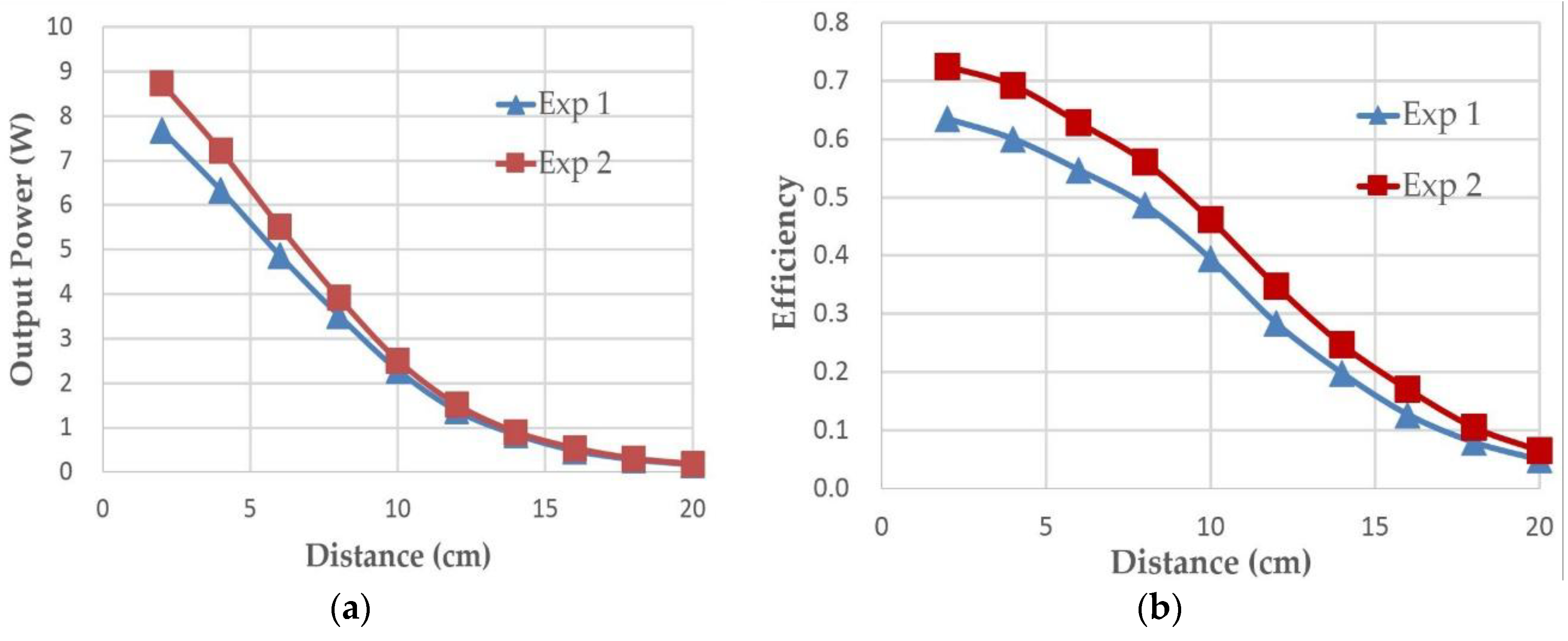
To better illustrate the difference between the three sets of measured data, we divided them into two comparison groups and depicted the output power and efficiency curves in Figure 13 and Figure 14, respectively. Specifically, the efficiency was computed as the ratio of the output power () to the input power (), which implies that it is the system efficiency, including the gate drive circuit, in Exp 1. Additionally, one thing to note is that the drive source power () was also accounted for in the input power when the two power sources were used in Exp 2 and Exp 3.
Figure 13a,b show the comparison of output power and efficiency between Exp 1 and Exp 2, respectively, and it is noted that the maximum output power and efficiency are 8.74 W and 72.5% with the improved inverter at a 2 cm separation distance, while the output power and efficiency are only 7.68 W and 63.5% with the traditional inverter at the same gap. The increase of output power in Figure 13a is obvious over a short distance due to the larger switching losses in the traditional inverter under heavy load. As the distance increase, the reflected impedance from the secondary side is too small to be neglected and the output power is almost the same due to Equation (17). The increase of system efficiency in Figure 13b is obvious in the bifurcation region for the lower gate losses and switching losses of the improved gate drive circuit. As the coil distance increases, the deviation of switching losses between Exp 1 and Exp 2 becomes less, while the gate losses remain constant, so the gap between the two efficiency curves decreases but does not merge together.
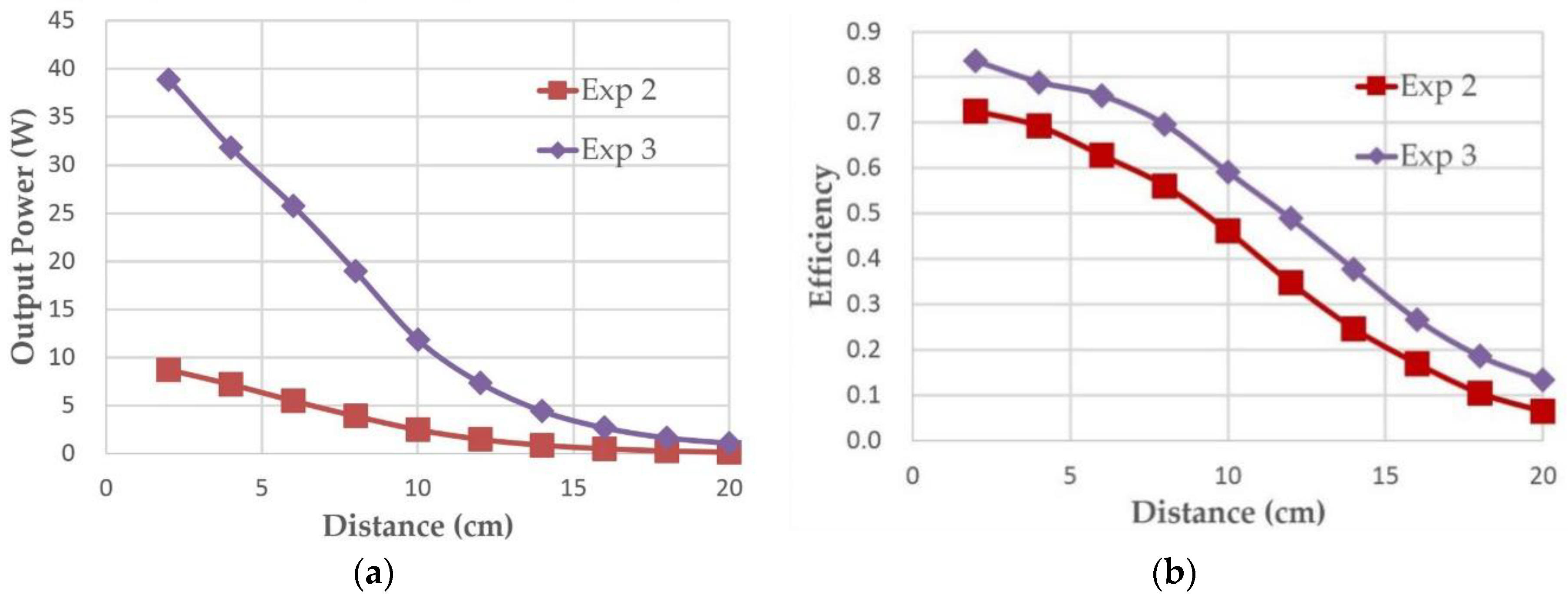
Figure 14a,b show the comparison of output power and efficiency between Exp 2 and Exp 3, respectively. It is clear that the output power of Exp 3 at a 2 cm separation distance is 38.9 W, which is about 4 times that in Exp 2, and the other data in Figure 14a have a similar rule, which is consistent with Equation (17). Meanwhile, Figure 14b shows that a higher efficiency of 83.6% can be acquired in Exp 3 compared with Exp 2 at the same gap, and the main reason is that the constant gate drive loss is nearly same as in Exp 2, and the switching loss makes up a far smaller percentage of the total losses in Exp 3.
For a better understanding, the losses of each block in Exp 1, Exp 2, and Exp 3 at 2 cm are summarized in Table 4.
Table 4 shows that the gate losses and switching losses make up a high percentage of the total losses in Exp 1, while the improved inverter reduces them significantly in Exp 2. Although the gate losses and switching losses make up a far smaller percentage in Exp 3, the losses caused by the parasitic resistances in the TX and RX tank increase rapidly and make up a relatively large percentage due to the large resonant current. Therefore, to further increase the efficiency of the improved system, more attention should be paid to low-loss inductors and capacitors.
6. Conclusions
This paper presents an improved autonomous current-fed push-pull parallel-resonant inverter in an IPT application. The inverter achieved a ZVS operation automatically as the coupling coefficient varied by tracking the ZPA frequencies of a parallel-parallel resonant circuit, which was analyzed mathematically and verified by experiments. Moreover, the improved inverter increases the output power level and the system efficiency by reducing the gate losses and switching losses. Accordingly, two groups of comparative experiments were performed and verified that the improved inverter can increase the output power from 7.68 W to 8.74 W and overall efficiency from 63.5% to 72.5% compared with the traditional inverter at a 2 cm coil distance. In addition, a higher power of 38.9 W and a higher efficiency of 83.6% can also be obtained by increasing the input voltage to 24 V at 2 cm, which implies that the improved inverter can be used in a variety of IPT applications, such as IMDs or high-voltage quick charge.
Author Contributions
Conceptualization, X.Z. and D.X.; Formal analysis, A.Y.; Investigation, A.Y.; Supervision, X.Z.; Validation, M.T. and J.L.; Writing—original draft, A.Y.; Writing—review & editing, X.Z. and D.X.
Funding
This research work was funded by the Natural Science Foundation of China grant number 61501065, 61701054, and 61601067, the National Natural Science Foundation of China grant number 61571069, and the Chongqing Research Program of Basic Research and Frontier Technology grant number cstc2016jcyjA0021.
Conflicts of Interest
The authors declare no conflict of interest.
References
- Covic, G.A.; Boys, J.T. Inductive power transfer. Proc. IEEE 2013, 101, 1276–1289. [Google Scholar] [CrossRef]
- Sample, A.P.; Meyer, D.A.; Smith, J.R. Analysis, experimental results, and range adaptation of magnetically coupled resonators for wireless power transfer. IEEE Trans. Ind. Electron. 2011, 58, 544–554. [Google Scholar] [CrossRef]
- Gallucci, L.; Menna, C.; Angrisani, L.; Asprone, D.; Moriello, R.S.L.; Bonavolontà, F.; Fabbrocino, F. An embedded wireless sensor network with wireless power transmission capability for the structural health monitoring of reinforced concrete structures. Sensors-Basel 2017, 17, 2566. [Google Scholar] [CrossRef] [PubMed]
- Wang, B.; Hu, A.P.; Budgett, D. Power flow control based solely on slow feedback loop for heart pump applications. IEEE Trans. Biomed. Circuits Syst. 2012, 6, 279–286. [Google Scholar] [CrossRef] [PubMed]
- Si, P.; Hu, A.P.; Malpas, S.; Budgett, D. A frequency control method for regulating wireless power to implantable devices. IEEE Trans. Biomed. Circuits Syst. 2008, 2, 22–29. [Google Scholar] [CrossRef] [PubMed]
- Ahn, D.; Hong, S. Wireless power transmission with self-regulated output voltage for biomedical implant. IEEE Trans. Ind. Electron. 2014, 61, 2225–2235. [Google Scholar] [CrossRef]
- Waters, B.H.; Sample, A.P.; Bonde, P.; Smith, J.R. Powering a ventricular assist device (VAD) with the free-range resonant electrical energy delivery (FREE-D) system. Proc. IEEE 2012, 100, 138–149. [Google Scholar] [CrossRef]
- Siqi, L.; Mi, C.C. Wireless power transfer for electric vehicle applications. IEEE J. Emerg. Select. Top. Power Electron. 2015, 3, 4–17. [Google Scholar] [CrossRef]
- Kamineni, A.; Covic, G.A.; Boys, J.T. Self-tuning power supply for inductive charging. IEEE Trans. Power Electron. 2017, 32, 3467–3479. [Google Scholar] [CrossRef]
- Sallan, J.; Villa, J.L.; Llombart, A.; Sanz, J.F. Optimal design of ICPT systems applied to electric vehicle battery charge. IEEE Trans. Ind. Electron. 2009, 56, 2140–2149. [Google Scholar] [CrossRef]
- Samanta, S.; Rathore, A.K. Analysis and design of load-independent ZPA operation for P/S, PS/S, P/SP, and PS/SP tank networks in IPT applications. IEEE Trans. Power Electron. 2018, 33, 6476–6482. [Google Scholar] [CrossRef]
- Low, Z.N.; Chinga, R.A.; Tseng, R.; Lin, J. Design and test of a high-power high-efficiency loosely coupled planar wireless power transfer system. IEEE Trans. Ind. Electron. 2009, 56, 1801–1812. [Google Scholar]
- Chwei-Sen, W.; Covic, G.A.; Stielau, O.H. Power transfer capability and bifurcation phenomena of loosely coupled inductive power transfer systems. IEEE Trans. Ind. Electron. 2004, 51, 148–157. [Google Scholar]
- Hsu, J.-U.W.; Hu, A.P. Determining the variable inductance range for an LCL wireless power pick-up. In Proceedings of the IEEE Conference on Electron Devices and Solid-State Circuits, Tainan, Taiwan, 20–22 December 2007; pp. 489–492. [Google Scholar]
- James, J.; Boys, J.; Covic, G. A variable inductor based tuning method for ICPT pickups. In Proceedings of the 7th International Power Engineering Conference, Singapore, 29 November–2 December 2005; pp. 1142–1146. [Google Scholar]
- Saad, M.; Alarcón, E. Insights into dynamic tuning of magnetic-resonant wireless power transfer receivers based on switch-mode gyrators. Energies 2018, 11, 453. [Google Scholar] [CrossRef]
- Tian, J.; Hu, A.P. A DC-voltage controlled variable capacitor for stabilizing the ZVS frequency of a resonant converter for wireless power transfer. IEEE Trans. Power Electron. 2016, 32, 2312–2318. [Google Scholar] [CrossRef]
- Schormans, M.; Valente, V.; Demosthenous, A. Frequency splitting analysis and compensation method for inductive wireless powering of implantable biosensors. Sensors-Basel 2016, 16, 1229. [Google Scholar] [CrossRef] [PubMed]
- Kim, N.Y.; Kim, K.Y.; Ryu, Y.H.; Choi, J.; Kim, D.Z.; Yoon, C.; Park, Y.K.; Kwon, S. Automated adaptive frequency tracking system for efficient mid-range wireless power transfer via magnetic resonanc coupling. In 2012 42nd European Microwave Conference; IEEE: New York, NY, USA, 2012; pp. 221–224. [Google Scholar]
- Hu, A.P.; Si, P. A Low Cost Portable Car Heater Based on a Novel Current-Fed Push-Pull Inverter; Australasian Univ. Power Eng. Conf. (AUPEC): Brisbane, Australia, 2004. [Google Scholar]
- Costanzo, A.; Dionigi, M.; Mastri, F.; Mongiardo, M. Rigorous modeling of mid-range wireless power transfer systems based on royer oscillators. In Proceedings of the Wireless Power Transfer (WPT), Perugia, Italy, 15–16 May 2013; pp. 69–72. [Google Scholar]
- Abdolkhani, A.; Hu, A.P. Improved autonomous current-fed push–pull resonant inverter. IET Power Electron. 2014, 7, 2103–2110. [Google Scholar] [CrossRef]
- Kazimierczuk, M.K.; Czarkowski, D. Resonant Power Converters; John Wiley & Sons: Hoboken, NJ, USA, 2012. [Google Scholar]
- Wang-Qiang, N.; Jian-Xin, C.; Wei, G.; Ai-Di, S. Exact analysis of frequency splitting phenomena of contactless power transfer systems. IEEE Trans. Circuits Syst. I Regul. Pap. 2013, 60, 1670–1677. [Google Scholar]
- Wang, B.; Hu, A.P.; Budgett, D. Maintaining middle zero voltage switching operation of parallel-parallel tuned wireless power transfer system under bifurcation. IET Power Electron. 2014, 7, 78–84. [Google Scholar] [CrossRef]
- Hu, A.P.; Covic, G.A.; Boys, J.T. Direct ZVS start-up of a current-fed resonant inverter. IEEE Trans. Power Electron. 2006, 21, 809–812. [Google Scholar] [CrossRef]
- Grover, F.W. Inductance Calculations: Working Formulas and Tables; Courier Corporation: Chelmsford, MA, USA, 2004. [Google Scholar]
- Imura, T.; Hori, Y. Maximizing air gap and efficiency of magnetic resonant coupling for wireless power transfer using equivalent circuit and neumann formula. IEEE Trans. Ind. Electron. 2011, 58, 4746–4752. [Google Scholar] [CrossRef]
Figure 1.
The schematic of a traditional autonomous current-fed push-pull inductive power transfer (IPT) system.
Figure 1.
The schematic of a traditional autonomous current-fed push-pull inductive power transfer (IPT) system.

Figure 2.
Equivalent circuit of current-fed push-pull parallel-resonant circuit.

Figure 3.
Operation principle of an ideal autonomous inverter at steady state.

Figure 4.
Simplified circuit model: (a) with sinusoidal current source and mutual voltage; (b) with reflected impedance.
Figure 4.
Simplified circuit model: (a) with sinusoidal current source and mutual voltage; (b) with reflected impedance.

Figure 5.
The impedance characteristic of Zp versus frequency: (a) phase angle; (b) real part.

Figure 6.
Voltage and current waveforms of a traditional circuit simulation at VDC = 12 V.

Figure 7.
The schematic of an improved autonomous current-fed push-pull IPT system.

Figure 8.
Voltage and current waveforms of the improved circuit simulation at VDC = 12 V.

Figure 9.
Voltage and current waveforms of the improved circuit simulation at VDC = 24 V and Vdrive = 12 V.
Figure 9.
Voltage and current waveforms of the improved circuit simulation at VDC = 24 V and Vdrive = 12 V.

Figure 10.
Photo of the experimental setup.

Figure 11.
Calculated and measured zero phase angle (ZPA) frequencies of a parallel-resonant circuit versus distance.
Figure 11.
Calculated and measured zero phase angle (ZPA) frequencies of a parallel-resonant circuit versus distance.

Figure 12.
Gate and drain voltage waveforms of two MOSFETs (metal oxide silicon field effect transistors) at 6 cm: (a) traditional inverter at VDC = 12 V (Exp 1); (b) improved inverter at VDC = Vdrive = 12 V (Exp 2); (c) improved inverter at VDC = 24 V and Vdrive = 12 V (Exp 3).
Figure 12.
Gate and drain voltage waveforms of two MOSFETs (metal oxide silicon field effect transistors) at 6 cm: (a) traditional inverter at VDC = 12 V (Exp 1); (b) improved inverter at VDC = Vdrive = 12 V (Exp 2); (c) improved inverter at VDC = 24 V and Vdrive = 12 V (Exp 3).


Figure 13.
Comparison of Exp 1 and Exp 2 versus distance: (a) output power; (b) system efficiency.

Figure 14.
Comparison of Exp 2 and Exp 3 versus distance: (a) output power; (b) system efficiency.


Table 1.
Parameters and components of a traditional circuit.
| L3 | 100 μH | Lchoke1, Lchoke2 | 100 μH |
| C1, C2 | 36.4 nF | D1, D2 | MBRS3100 |
| R1, R2 | 100 Ω | R3, R4 | 10 kΩ |
| Ds1–Ds4 | MBRS3100 | C3 | 22 μF |
| M1, M2 | IRFP250N | Rload | 50 Ω |
Table 2.
Parameters of the primary and secondary side coils L1 and L2.
| Parameters | Symbol | TX Coil | RX Coil |
|---|---|---|---|
| Inductance | L | 1.6 μH | 1.6 μH |
| Number of turns | N | 2 | 2 |
| Diameter of the coil | dc | 176 mm | 176 mm |
| Diameter of the wire | dw | 3 mm | 3 mm |
Table 3.
Parameters and components of the improved circuit.
| L3 | 100 μH | Lchoke1, Lchoke2 | 100 μH |
| C1, C2 | 36.4 nF | D2, D4 | MBRS3100 |
| R1, R4 | 1 kΩ | R2, R3 | 10 kΩ |
| Ds1–Ds4 | MBRS3100 | C3 | 22 μF |
| D1, D3 | SS310 | Rload | 50 Ω |
| M1, M2 | IRFP250N | Q1, Q2 | ZXTN25040 |
Table 4.
Power losses and the corresponding percentage of each block in Exp 1, Exp 2, and Exp 3.
| Experiments | Gate Drive | Switches | TX Tank | RX Tank | Others |
|---|---|---|---|---|---|
| Exp 1 | 1.77 W (40%) | 1.33 W (30%) | 0.53 W (12%) | 0.40 W (9%) | 0.40 W (9%) |
| Exp 2 | 1.35 W (41%) | 0.40 W (12%) | 0.66 W (20%) | 0.50 W (15%) | 0.39 W (12%) |
| Exp 3 | 1.45 W (19%) | 0.69 W (9%) | 2.60 W (34%) | 1.99 W (26%) | 0.91 W (12%) |
© 2018 by the authors. Licensee MDPI, Basel, Switzerland. This article is an open access article distributed under the terms and conditions of the Creative Commons Attribution (CC BY) license (http://creativecommons.org/licenses/by/4.0/).
Share and Cite
MDPI and ACS Style
Yu, A.; Zeng, X.; Xiong, D.; Tian, M.; Li, J. An Improved Autonomous Current-Fed Push-Pull Parallel-Resonant Inverter for Inductive Power Transfer System. Energies 2018, 11, 2653. https://doi.org/10.3390/en11102653
AMA Style
Yu A, Zeng X, Xiong D, Tian M, Li J. An Improved Autonomous Current-Fed Push-Pull Parallel-Resonant Inverter for Inductive Power Transfer System. Energies. 2018; 11(10):2653. https://doi.org/10.3390/en11102653
Chicago/Turabian StyleYu, Anning, Xiaoping Zeng, Dong Xiong, Mi Tian, and Junbing Li. 2018. "An Improved Autonomous Current-Fed Push-Pull Parallel-Resonant Inverter for Inductive Power Transfer System" Energies 11, no. 10: 2653. https://doi.org/10.3390/en11102653
Note that from the first issue of 2016, this journal uses article numbers instead of page numbers. See further details here.