Design and Controller-In-Loop Simulations of a Low Cost Two-Stage PV-Simulator
by
 , and
, and
Sridhar Vavilapalli
1, 
Umashankar Subramaniam
1,
Sanjeevikumar Padmanaban
2,* and
and
Frede Blaabjerg
3 1
Department of Energy and Power Electronics, School of Electrical Engineering, VIT University, Vellore 632014, India
2
Department of Energy Technology, Aalborg University, 6700 Esbjerg, Denmark
3
Center of Reliable Power Electronics (CORPE), Department of Energy Technology, Aalborg University, 9100 Aalborg, Denmark
*
Author to whom correspondence should be addressed.
Energies 2018, 11(10), 2774; https://doi.org/10.3390/en11102774
Submission received: 2 September 2018
/
Revised: 27 September 2018
/
Accepted: 3 October 2018
/
Published: 16 October 2018
(This article belongs to the Special Issue Multilevel Converters: Analysis, Modulation, Topologies, and Applications)
Abstract
:A PV-Simulator is a DC power source in which the current-voltage (I-V) characteristics of different PV arrays can be programmed. With a PV-simulator, the operation of the solar power conditioning systems can be validated at a laboratory level itself before actual field trials. In this work, design, operation and controls for a two-stage programmable PV-simulator required for the testing of solar power conditioning systems are presented. The proposed PV-simulator consists of a three-level T-type active front-end converter in the first stage and a buck-chopper-based DC-DC converter in the second stage. An active front-end rectifier using a three-level T-type IGBT-based converter is used at the input stage to help in operating the system at unity power factor. A DC-DC converter at the output stage of the simulator is regulated to obtain the I-V characteristics of the programmed PV-Array. Hardware-In-Loop simulations are carried out to validate the proposed system and the associated controls implemented in the controller. As a case study, this PV-simulator is programmed with electrical parameters of a selected PV-array and the characteristics obtained from the PV-simulator are compared with the actual PV-array characteristics. The dynamic response of the system for sudden changes in the load and sudden changes in irradiance values are studied.
1. Introduction
The operation and efficiency of a solar power conditioning system at different operating points can be tested using a variable DC source in the laboratory, but to validate the ability to track the maximum power point (MPP) in the power conditioning system, it is necessary to test the system with an actual PV array, but with an actual PV array, it is difficult to test the system at predefined operating points due to varying climatic changes. The space and cost required for the installation of an actual PV array are also more. With an actual PV array on site, it is necessary to alter the series/parallel combination of PV modules for testing different rated PV power conditioning systems. Hence a PV simulator is required to validate the solar power conditioning system at the laboratory level itself before any actual site trials [1,2]. A PV-simulator system is a DC power source in which the current-voltage (I-V) characteristics of different PV arrays can be programmed so that the operation of the solar power conditioning system can be validated. With a PV-simulator, it is possible to test the power conditioning systems for different voltage current combinations within the rated values of the PV-simulator.
An LLC resonant DC-DC converter-based PV-simulator discussed in [3,4] consists of a current driven centre tapped transformer which provides galvanic isolation between input and output circuits. A PV-simulator based on an interleaved buck converter is presented in [5,6]. A buck-boost chopper-based PV-simulator with double current mode control is proposed in [7] and a buck chopper-based PV-simulator with a two stage LC filter is discussed in [8]. A PV-simulator based on a two-quadrant DC-DC converter is proposed in [9]. A buck-chopper-based DC-DC converter with a single stage L-C filter is presented in [10,11,12]. The above discussed configurations and the components required for each configuration are summarized in Table 1 and it is observed that the buck-chopper-based PV-simulator is the most economical compared to other configurations due to its lesser number of magnetic components and power switches.
In the works discussed in [4,5,6,7,8,9,10,11,12], a DC source is considered as input, hence the AC to DC conversion stage is not discussed. A PV-simulator manufactured by M/s Chroma with type number 62000H-S series, is suitable for the input sources such as single-phase 220 Vac and three-phase 440 Vac which are usually available at laboratories. This simulator is suitable for the testing of inverters up to the rating of 1000 V, 25 A. Multiple such PV simulators can be connected for testing of higher rated power conditioning systems. Since AC is the commonly available supply in laboratories, it is preferred to have a rectifier at the input stage of the PV simulator.
A PV-simulator with an AC input source presented in [13,14] consists of a single phase diode front end rectifier and a buck chopper-based DC-DC converter. Due to the uncontrolled single phase diode rectifier in the input section, the input THD and power factor are poor with the presented configuration. To make the system operate at unity power factor with a better THD, it is desirable to have an active front end rectifier in the input stage. A three level front end converter is preferable over a conventional two level inverter as the total power loss in a three-level converter is comparatively lesser than that of a two-level converter [15,16]. Also the voltage and current harmonics in a three-level converter are comparatively lesser than those of a two-level converter [17]. The dv/dt in a three-level converter is less than that of a two-level inverter; hence the voltage stresses on the devices are also minimized. Three-level front-end converters can be designed either with a diode clamped converter or a T-type converter. A T-type three-level converter is suitable for low voltage applications as the switching and conduction losses in T-type three-level converters are less compared to that of a diode clamped three level inverter [18]. Due to the above advantages a front-end converter based on a T-type configuration is selected in this work.
In this work, the design of a low cost PV-simulator with a single phase front end converter and a buck-chopper-based DC-DC converter is proposed. The block diagram of the proposed simulator is shown in Figure 1. Parameters such as open-circuit voltage, short-circuit current, MPP voltage, MPP current, power rating, series resistance, parallel resistance and temperatures coefficients of the selected PV array which are usually available from the product datasheet and can be programmed in the PV-simulator. The variable inputs such as irradiance on the PV array and the temperature of PV array can be varied from the user interface for testing the power conditioning system at various operating points. The maximum ratings of the PV array that can be programmed are restricted to the rated output voltage and currents of PV-simulator.
Due to the advantages of a T-type configuration over a conventional two-level converter mentioned earlier, a front-end converter based on a T-type configuration is selected in the present work. The control philosophy for a single phase active front-end rectifier is presented in [19]. Closed loop voltage control is adapted to regulate the DC link voltage. Closed loop voltage control for a three-phase active front-end rectifier is discussed in [20]. Reference DC link voltage for FEC is always adjusted more than the open circuit voltage of the programmed PV array. An isolation transformer is used at the input side of the simulator. The isolation transformer enables the operation of multiple PV-simulators connected in parallel for testing of higher rated solar power conditioning systems. The input inductance required for the boosting operation of front-end rectifier can be incorporated in the transformer itself so that the component count, cost and weight can be minimized.
The second stage of power conversion consists of a buck-chopper-based DC-DC converter. The output voltage of the chopper ranges between the minimum PV voltage i.e., zero and the maximum PV voltage i.e., the open circuit voltage of the programmed PV array. Current control is adapted for the DC-DC converter to replicate the I-V characteristics of programmed PV array. Reference output current is obtained from the programmed PV parameters, while irradiance input, and operating temperature input are adjusted by the user and the instantaneous output voltage. In this work, the PV-simulator is designed to be programmed up to the ratings of the selected PV array shown in Table 2. A PV array comprised of multiple PV modules (Type number SPR-435NE-WHT-D of M/s Sun Power) connected in series-parallel combination is considered. The T-type front-end converter, buck-chopper-based DC-DC converter and its controls are discussed in detail. Real-time simulations are carried out to validate the system using an Opal-RT brand real-time simulator. I-V characteristics obtained from the PV-simulator are compared with the actual PV-array characteristics to validate the controls.
2. A Three-Level T-Type Front-End Rectifier
As the input to the PV-simulator is an AC source, a rectifier is to be used on the input stage. Instead of using an uncontrolled diode rectifier, an active front-end converter (FEC) is proposed in this system to obtain unity power factor on the input side. A three-level T-Type FEC is selected over a conventional two-level H-bridge-based FEC to obtain better input THD and low dv/dt. A transformer is also proposed on the input side for isolation purposes in the present work. The input inductance required for the boost operation can also be incorporated in the input transformer. The isolation transformer also enables the parallel operation of multiple PV-simulators during the testing of higher rated power conditioning systems. Since the open-circuit voltage of the PV-array selected is 342 V, the DC link voltage (Vdc) should always be more than the open circuit voltage i.e., 342 V. In the present system, Vdc selected is 500 V i.e., approximately 1.5 times the open-circuit voltage of the PV-array. Commercially available power conditioning systems are listed in [21] and it is observed that the maximum PV voltages are in the range of 1000 V to 1500 V DC. The proposed system can be extended to higher voltages by suitably selecting the turn ratio of the input transformer. The power rating of the FEC should be more than the maximum power rating of the PV-array. By considering the efficiency of the PV-simulator as 85%, the power rating of the FEC obtained is 20.5 kW.
The power circuit and the control block diagram for the proposed FEC are shown in Figure 2. The controller monitors the input AC voltage and using a phase locked loop (PLL), a unit signal which is in-phase with the input voltage is generated. The reference DC link voltage (Vdc_ref) is adjusted to 500 V in this system and actual DC link voltage (Vdc) is monitored and the error is applied to a PI controller. A feedforward control is used for improving the dynamic response of the system to sudden changes in DC current (Idc). The output of the feed-forward loop is multiplied with the unit signal to obtain the reference input current. The reference AC current is compared with the actual AC current and the error is applied to a PI controller to obtain the modulating signal for the rectifier. The dynamic response of the system can be studied by applying a step change in reference DC voltage (Vdc_Ref) and the load current (Idc) [22].
Operation of FEC and the dynamic response of the system are validated through real-time simulations using an Opal RT real-time simulator. The electrical scheme for real-time simulation validation is shown in Figure 3. In this setup, the plant, comprised of an input supply, transformer, T-Type converter, DC-link capacitors, and the load are modeled in Matlab-Simulink with a sample time of 10 microseconds. The simulated model is compiled and loaded in the high speed processor of the real-time simulator. The control software for T-type front end converter is developed through a Matlab embedded coder and loaded in the controller card based on a Texas Instruments TMS320F2812 digital single processor. Details of the controller card used and the real-time simulator are shown in Table 3.
Start/Stop commands are given to the controller from external pushbuttons. The DC link voltage reference VDC_Ref signal is also given from user interface to the analog input channel of the controller card. Using the analog output channels of the real-time simulator, the voltage and current signals from the plant are given to the analog input channels of the controller card.
The controller card provides gate signals for the FEC through the digital input channels of the real-time simulator. A simulated ‘Stack faulty signal’ in the plant is given to the controller card through the digital output channel of the real-time simulator. On receiving the stack faulty signal from the plant, the controller blocks the gate pulses to the FEC and also provides an off command to the input AC breaker Q1. To provide step changes in the load, two contactors Q2, Q3 are simulated and the control signals for these load switches are provided by the controller through the digital input channels of the real-time simulator. The dynamic response of the FEC is observed for sudden changes in the DC link voltage reference (VDC_Ref) and for sudden changes in load.
2.1. Dynamic Response of FEC for a Step Change in Vdc_Ref
A fixed resistive load is connected across the output DC terminals of FEC and a Vdc_ref is adjusted to 500 V. Since a T-type configuration is used, the PWM voltage at the rectifier AC terminals has three levels. The voltage step in the PWM voltage is equal to half of the value of the DC link voltage as shown in Figure 4a. Since the FEC maintains unity power factor, the input voltage and current are in-phase with each other, as shown in Figure 4b. A step change in the reference DC link voltage is applied and it is observed that the actual DC link voltage follows the reference DC voltage. Since the new Vdc_Ref is 600 volts, the voltage step in the three-level PWM voltage also varied and becomes 300 volts, i.e., half of the DC link voltage as shown in Figure 4a. Since a fixed resistive load is connected across DC terminals of the FEC, the load current also increases which results in an increase in the input side current. It is observed that the input current is also increased but still maintains the unity power factor as shown in Figure 4b.
2.2. Dynamic Response of FEC for a Step Change in Idc
In this case, the reference DC link voltage is maintained at 600 volts and a step change in the load is applied. Since the Vdc ref is 600 volts, the DC link voltage is 600 volts and the voltage step in the three-level PWM voltage is 300 volts, i.e., half of the DC link voltage as shown in Figure 5a. FEC is operating at unity power factor, hence the input voltage and current are in-phase with each other as shown in Figure 5b.
A step change in DC load is applied and it is observed that the actual DC link voltage drops by approximately 40 volts at that instant and increases gradually to the reference value, i.e., 600 volts, as shown in Figure 5a. Since the load is increased on the DC side, there in an increase in the input side current. It is observed that the input current is increased but the unity power factor is still maintained as shown in Figure 5b.
From the presented real-time simulation results, it is observed that the FEC controls programmed in the real controller are satisfactory as the system operation is as desired under different operating conditions. The dynamic response of the system and the associated controls are also good as the settling time and overshoots are less. For PV-simulator applications, the reference DC link voltage of the FEC is always adjusted to be more than the open circuit voltage of the programmed PV array. The FEC always operates at unity power factor and the input current depends on the DC-DC converter operation which is connected as load to the FEC. Detailed discussions on DC-DC converter and associated controls are presented in the next section.
3. Buck-Chopper-Based DC-DC Converter
The current-voltage (I-V) characteristics of a programmed PV array are realized through a DC-DC converter in the PV-simulator. A buck-chopper based DC-DC converter is used in this work and the closed loop current control is applied, to make the buck-chopper work like a current source similar to a PV array. Reference output current (I_PV_Ref) is compared with actual output current (I_PV) and the error signal is applied to PI controller to obtain the reference duty cycle for the chopper. A hysteresis controller can also be adapted for the current control through buck-chopper. The PWM block generates the gate pulse for the chopper. The detailed control block diagram is as shown in Figure 6.
In this work, the reference DC current is obtained from the PV current equation given in [11] as shown in Equation (1):
where I = PV current, V = PV voltage, Isc = short circuit current and Voc = Open circuit Voltage
where Iro = measured irradiance (1000 W/m2), RSe = series resistance, RP = parallel resistance and N is the quality factor
where Boltzmann’s constant (k) = 1.3806 × 10⁻²³, operating temperature (T) = 25 °C and the charge of an electron (q) = 1.602 × 10⁻¹⁹.
I_PV_Ref = Iph − (Is*(e (V + I*Rse)/N*Vt−1))) − ((V + I*Rse)/Rp)
Photon current Iph = Irradiance X (Isc/Iro)
Saturation current Is = Isc/(exp(Voc/(N*Vt))−1)
Thermal voltage Vt = k*T/q
Irradiance and temperature of PV array signals are adjustable by the user in this PV-simulator to test the solar power conditioning system under different operating conditions. To verify the operation of the PV-simulator, a PV array with the specifications listed in Table 4 and the proposed PV-simulator circuit are simulated for the same operating conditions and compared with each other.
The PV array and the PV-simulator are simulated in two different cases. In case-1, load resistance is maintained constant and the irradiance value is varied in steps. In case-2, irradiance is kept constant and the load resistance is varied.
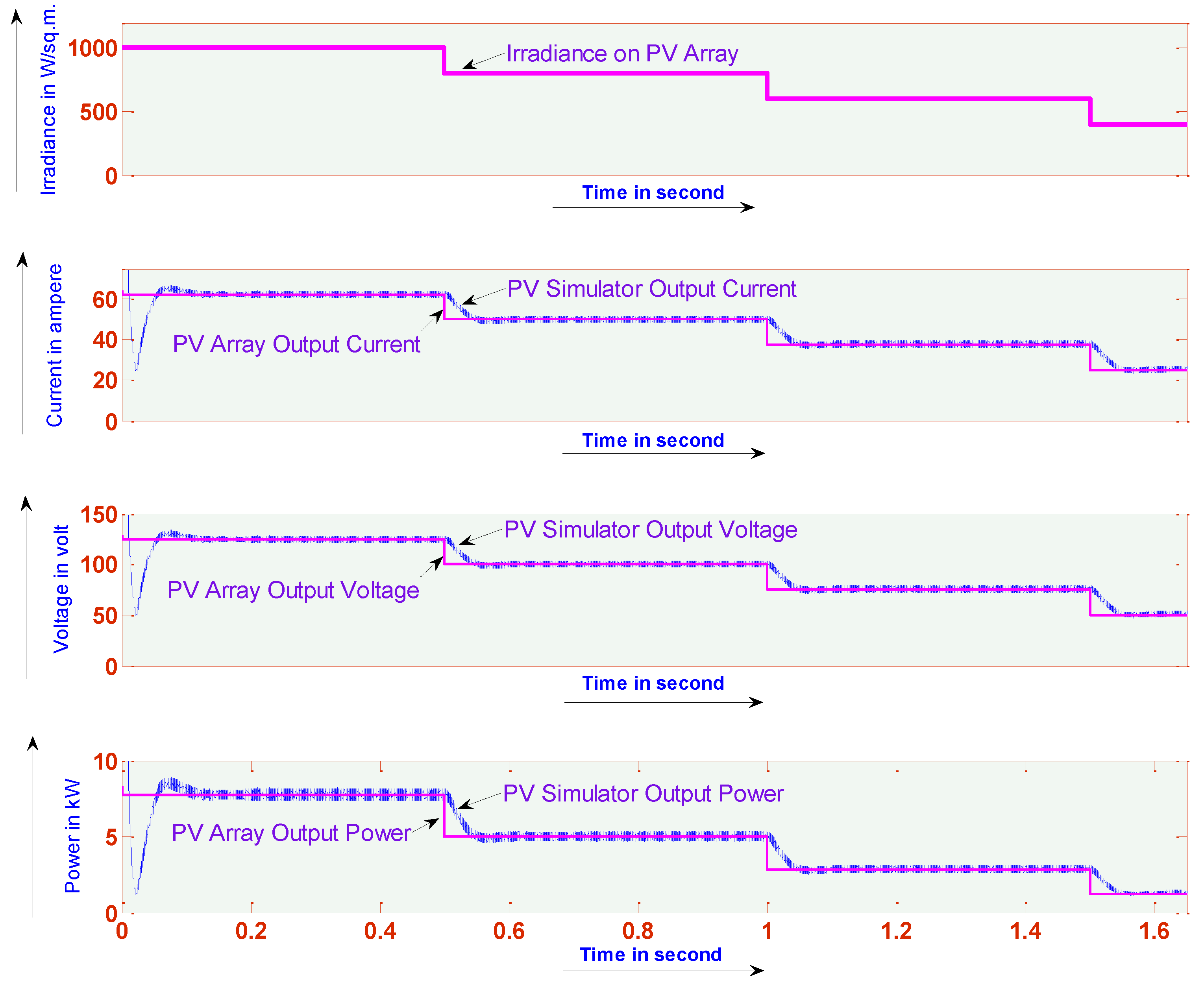
Case-1: A fixed resistive load is connected to the PV array and the PV-array output voltage, current and power are monitored by varying the irradiance. PV current is proportional to the irradiance and the PV voltage is the product of PV current and the load resistance. Similarly the PV-simulator is also connected to the same load and tested for the same conditions to compare the results with the results obtained by simulating a PV array. It is observed that the outputs of PV array and the PV-simulator match with each other as shown in Figure 7. Irradiance input to the simulator is reduced in steps of 200 W/sq.m at each 0.5 s time and it is observed that the reference current to the chopper is also reduced proportionally to the irradiance. The controller ensures the actual output current remains equal to the reference output current with the help of a closed-loop current controller.
Case-2: An irradiance of 600 W/Sq.m is applied as input to both the PV array and PV-simulator. Table 3 shows the parameters of the PV array at 600 W/sq.m which are derived based on the parameters in the datasheet of the PV module (Type number SPR-435NE-WHT-D of M/s Sun Power) selected. Independent variable loads are connected to PV array and the PV-simulator outputs. Loads on the PV-Array and the PV-simulator are increased in steps and monitored the output voltages, currents and powers. From the results shown in Figure 8, it is observed that the output values obtained from the PV-simulator are identical to the values obtained from the PV array.
4. Real-Time Simulation Results
To validate the controls for the proposed PV-simulator, controller in loop simulations are carried out with the help of an Opal-RT real-time simulator similar to the method presented in Section 2. The details of the hardware used for controller-in-loop simulations are listed in Table 3 and the scheme for the controller in loop simulations is shown in Figure 9.
The plant, comprised by an input source, FEC, DC-DC converter, and the load are modeled in Matlab-Simulink with a sample time of 10 microseconds and loaded into the real-time simulator. The control software is developed through Matlab embedded coder and the loaded in the DSP-based controller card. Start/Stop commands are given to the controller from external pushbuttons. Irradiance input and the temperature of PV array signals generated with the help of potentiometers and given to the analog input channels of the controller card. The controller card also receives the analog signals required from the plant such as input voltage, input current, output voltage and output currents from the simulated plant through the analog out (AO) channels of the real-time simulator.
As discussed in previous sections, on receiving the actual analog signals from the plant, the controller generates the gate pulses to maintain the actual values equal to the reference values for both FEC and DC-DC converters.The controller provides the gGate pulses to the simulated FEC and DC-DC converter through the digital input channels of the real-time simulator. The real-time simulator converts the gate pulses received into data to trigger the IGBTs. All this process happens with real-time speed.
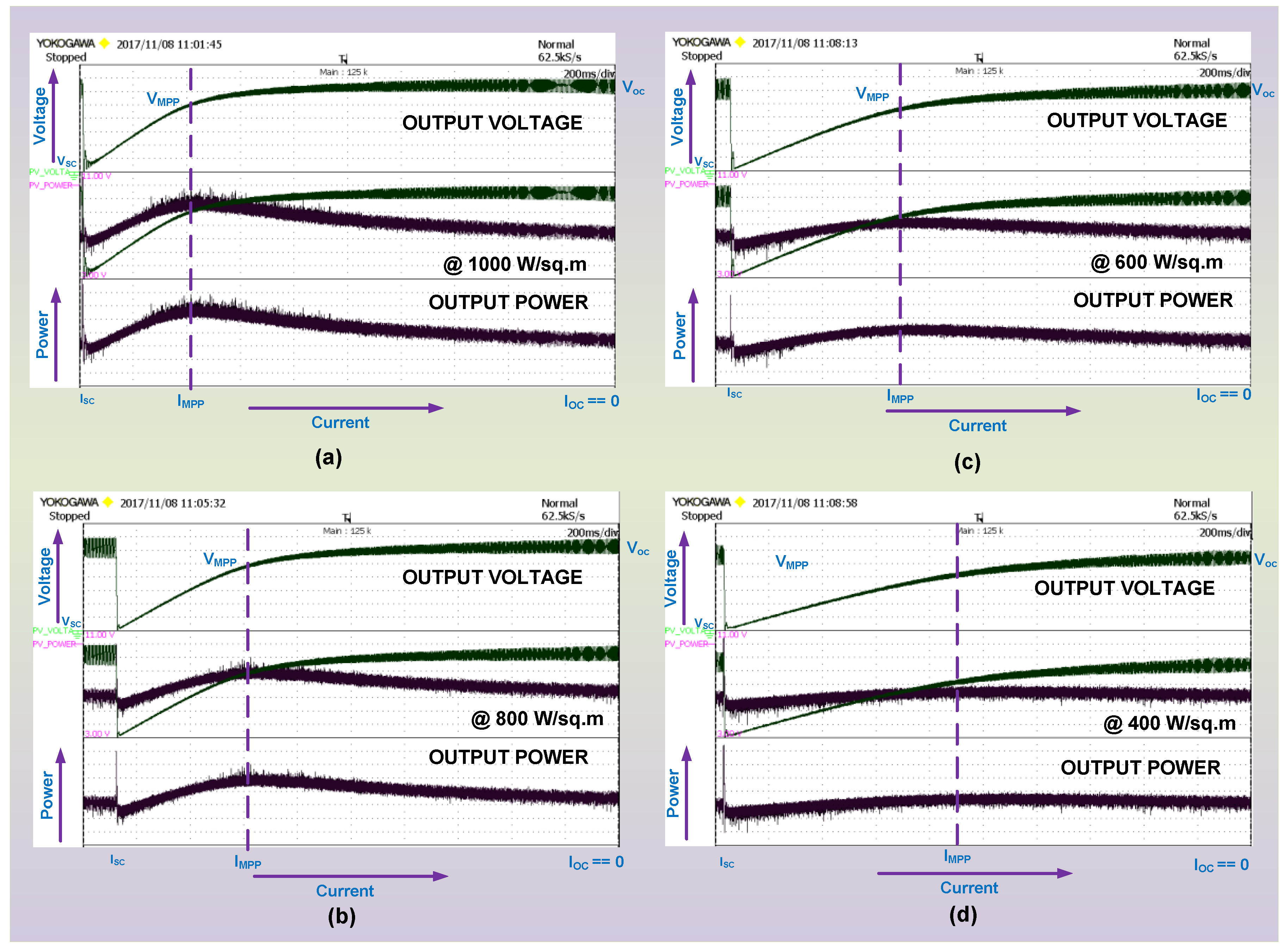
In this work, the PV array with the parameters shown in Table 4 are programmed in the PV-simulator and the load current is varied from short circuit current to zero current. The voltage and power of the PV array are monitored for different irradiance Inputs. From the presented results shown in Figure 10, it is observed that for different irradiance inputs, the MPP voltage is almost constant with a value of approximately 250 volts. The MPP voltages and powers obtained from the PV-simulator at different irradiance inputs are compared with the PV module datasheet (SPR-435NE-WHT-D) and it is found that the proposed PV-simulator can replicate the actual PV array characteristics.
5. Future Scope
In the present work, operation of a PV-simulator is validated through controller in loop simulations by interfacing the real controller hardware with the simulated power circuit by using a real-time simulator. Through controller-in-loop simulations, tuning of control software and the power circuit parameters is carried out. As a future work, it is envisaged to build a PV-simulator based on the present work.
A dual-active bridge (DAB)-based DC-DC converter with high frequency transformer presented in [23] is also investigated along with the chopper-based DC-DC converter for the present application. As a future work, it is envisaged to study a DAB-based PV-simulator to reduce the size of the equipment.
6. Conclusions
The proposed PV-simulator configuration provides better input THD as the front-end converter of a three-level rectifier. Unity power factor operation is achieved with this configuration which results in an optimized power rating of the simulator. FEC also helps in boosting the DC link voltage without using a step-up transformer on the AC side which results in lesser cost. From the presented results it can be concluded that the dynamic response of the system is satisfactory for sudden changes in load, sudden changes in the irradiance inputs and sudden changes in the DC link voltage reference. Instead of using an isolation transformer on the input side, it is also feasible to use a high-frequency transformer in the DC-DC converter which can reduce the size of the simulator. With the proposed configuration, multiple numbers of PV simulators can be connected in parallel for testing higher rated power conditioning systems. Operation of two PV-simulators connected in parallel subjected to unequal irradiance inputs can be studied which should help in analyzing the system operation during partial shading conditions.
Author Contributions
S.V., S.P., U.S., had developed the original proposed research work and implemented with numerical simulation software and real time RTDS system for investigation and performance validation. F.B. contributed his expertise in the proposed subject of research and verification of the obtained results based on theoretical concepts and insight background. All authors involved to articulate the research work for its final depiction as research paper.
Conflicts of Interest
The authors declare no conflict of interest.
References
- Jin, S.; Zhang, D.; Wang, C. UI-RI Hybrid Lookup Table Method with High Linearity and High-Speed Convergence Performance for FPGA-Based Space Solar Array Simulator. IEEE Trans. Power Electron. 2018, 33, 7178–7192. [Google Scholar] [CrossRef]
- Zhou, Z.; Macaulay, J. An Emulated PV Source Based on an Unilluminated Solar Panel and DC Power Supply. Energies 2017, 10, 2075. [Google Scholar] [CrossRef]
- Chang, C.; Chang, E.; Cheng, H. A High-Efficiency Solar Array Simulator Implemented by an LLC Resonant DC–DC Converter. IEEE Trans. Power Electron. 2013, 28, 3039–3046. [Google Scholar] [CrossRef]
- Chang, C.H.; Cheng, C.A.; Cheng, H.L. Modeling and design of the LLC resonant converter used as a solar-array simulator. IEEE J. Emerg. Sel. Top. Power Electron. 2014, 2, 833–841. [Google Scholar] [CrossRef]
- Mahmud, M.H.; Zhao, Y.; Wang, L. A high-bandwidth PV source simulator using a sliding mode controlled interleaved buck converter. In Proceedings of the IEEE International Conference IECON, Beijing, China, 29 October–1 November 2017; pp. 2326–2331. [Google Scholar]
- Koran, A.; LaBella, T.; Lai, J.S. High efficiency photovoltaic source simulator with fast response time for solar power conditioning systems evaluation. IEEE Trans. Power Electron 2014, 29, 1285–1297. [Google Scholar] [CrossRef]
- Zhang, W.; Kimball, J.W. DC–DC Converter Based Photovoltaic Simulator with a Double Current Mode controller. IEEE Trans. Power Electron. 2018, 33, 5860–5868. [Google Scholar] [CrossRef]
- Koran, A.; Sano, K.; Kim, R.Y.; Lai, J.S. Design of a Photovoltaic Simulator with a Novel Reference Signal Generator and Two-Stage LC Output Filter. IEEE Trans. Power Electron. 2010, 25, 1331–1338. [Google Scholar] [CrossRef]
- Cordeiro, A.; Foito, D.; Pires, V.F. A PV panel simulator based on a two quadrant DC/DC power converter with a sliding mode controller. In Proceedings of the IEEE International Conference on Renewable Energy Research and Applications (ICRERA), Padova, Italy, 22–25 November 2015; pp. 928–932. [Google Scholar]
- Kawano, M.; Sato, T.; Taguchi, T.; Genzima, Y.; Teramoto, S. Simple and low cost PV simulator using diode characteristics for development of PV system. In Proceedings of the INTELEC 2015—IEEE International Conference on Telecommunications Energy, Osaka, Japan, 18–22 October 2015; pp. 1–5. [Google Scholar]
- Özden, Ö.; Duru, Y.; Zengin, S.; Boztepe, M. Design and implementation of programmable PV simulator. In Proceedings of the IEEE International Conference on Fundamentals of Electrical Engineering (ISFEE), Bucharest, Romania, 30 June–2 July 2016; pp. 1–5. [Google Scholar]
- Seo, Y.T.; Park, J.Y.; Choi, S.J. A rapid IV curve generation for PV model-based solar array simulators. In Proceedings of the IEEE International Conference on Energy Conversion Congress and Exposition (ECCE), Milwaukee, WI, USA, 18–22 September 2016; pp. 1–5. [Google Scholar]
- Shinde, U.K.; Kadwane, S.G.; Keshri, R.K.; Gawande, S.P. Dual Mode Controller-Based Solar Photovoltaic Simulator for True PV Characteristics. Can. J. Electr. Comput. Eng. 2017, 40, 237–245. [Google Scholar]
- Piao, Z.G.; Gong, S.J.; An, Y.H.; Cho, G.B. A study on the PV simulator using equivalent circuit model and look-up table hybrid method. In Proceedings of the IEEE International Conference on Electrical Machines and Systems (ICEMS), Busan, Korea, 26–29 October 2013; pp. 2128–2131. [Google Scholar]
- Alemi, P.; Lee, D.C. Power loss comparison in two-and three-level PWM converters. In Proceedings of the IEEE International Conference on Power Electronics and ECCE Asia (ICPE & ECCE), Jeju, Korea, 30 May–3 June 2011; pp. 1452–1457. [Google Scholar]
- Schweizer, M.; Friedli, T.; Kolar, J.W. Comparative evaluation of advanced three-phase three-level inverter/converter topologies against two-level systems. IEEE Trans. Ind. Electron. 2013, 60, 5515–5527. [Google Scholar] [CrossRef]
- Masisi, L.; Choudhury, A.; Pillay, P.; Williamson, S. Performance comparison of a two-level and three-level inverter permanent magnet synchronous machine drives for HEV application. In Proceedings of the IEEE International Conference on Industrial Electronics Society (IECON), Vienna, Austria, 10–13 November 2013; pp. 7262–7266. [Google Scholar]
- Shin, H.; Lee, K.; Choi, J.; Seo, S.; Lee, J. Power loss comparison with different PWM methods for 3L-NPC inverter and 3L-T type inverter. In Proceeding of the IEEE Power Electronics and Application Conference and Exposition (PEAC), Shanghai, China, 5–8 November 2014; pp. 1322–1327. [Google Scholar]
- Labaki, R.; Kedjar, B.; Al-Haddad, K. Single-Phase Active Front End Converter with series compensation. In Proceedings of the IEEE International Symposium on Industrial Electronics, Montreal, QC, Canada, 9–13 July 2006; pp. 769–774. [Google Scholar]
- Huerta, F.; Stynski, S.; Cobreces, S.; Malinowski, M.; Rodriguez, F.J. Novel Control of Three-Phase Active Front-End Converter with Compensation of Unknown Grid-Side Inductance. IEEE Trans. Ind. Electron. 2011, 58, 3275–3286. [Google Scholar] [CrossRef]
- Sridhar, V.; Umashankar, S. A comprehensive review on CHB MLI based PV inverter and feasibility study of CHB MLI based PV-STATCOM. Renew. Sustain. Energy Rev. 2017, 78, 138–156. [Google Scholar] [CrossRef]
- Hou, C.C.; Cheng, P.T. Experimental Verification of the Active Front-End Converters Dynamic Model and Control Designs. IEEE Trans. Power Electron. 2011, 26, 1112–1118. [Google Scholar] [CrossRef]
- Sridhar, V.; Sanjeevikumar, P.; Umashankar, S.; Mihet-Popa, L. Power Balancing Control for Grid Energy Storage System in Photovoltaic Applications-Real Time Digital Simulation Implementation. Energies J. 2017, 10, 928. [Google Scholar]
Figure 1.
Block diagram of the proposed PV-Simulator.
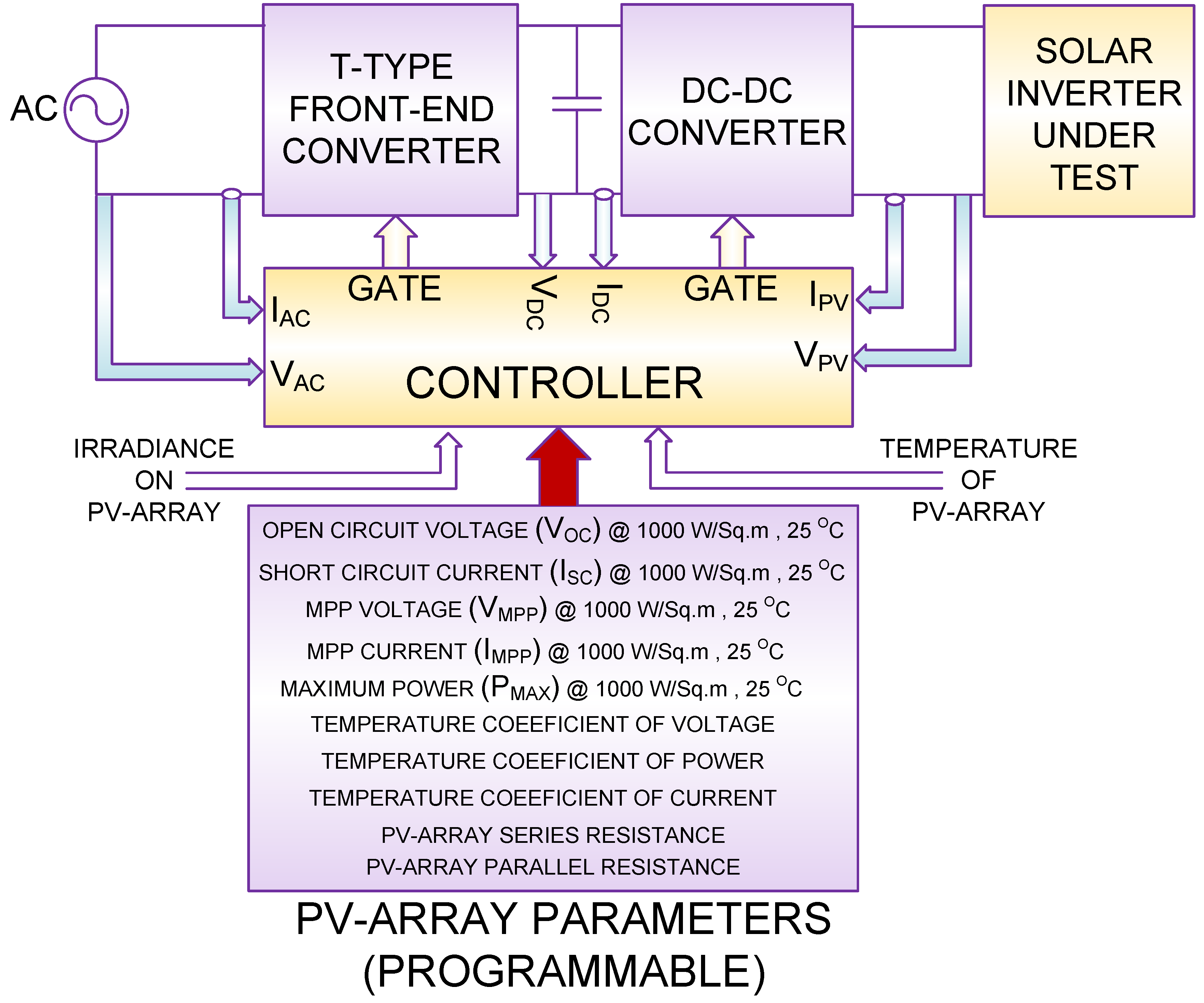
Figure 2.
Control Block diagram of T-Type Front-End Converter.

Figure 3.
Electrical scheme for controller-In-Loop simulation validation of T-Type Front-End Converter.
Figure 3.
Electrical scheme for controller-In-Loop simulation validation of T-Type Front-End Converter.

Figure 4.
(a) Voltage and Current Waveforms of T-Type Front-End Converter (b) Input Voltage and Current Waveforms of Front-End Converter during Transition time for a step change in DC link voltage.
Figure 4.
(a) Voltage and Current Waveforms of T-Type Front-End Converter (b) Input Voltage and Current Waveforms of Front-End Converter during Transition time for a step change in DC link voltage.
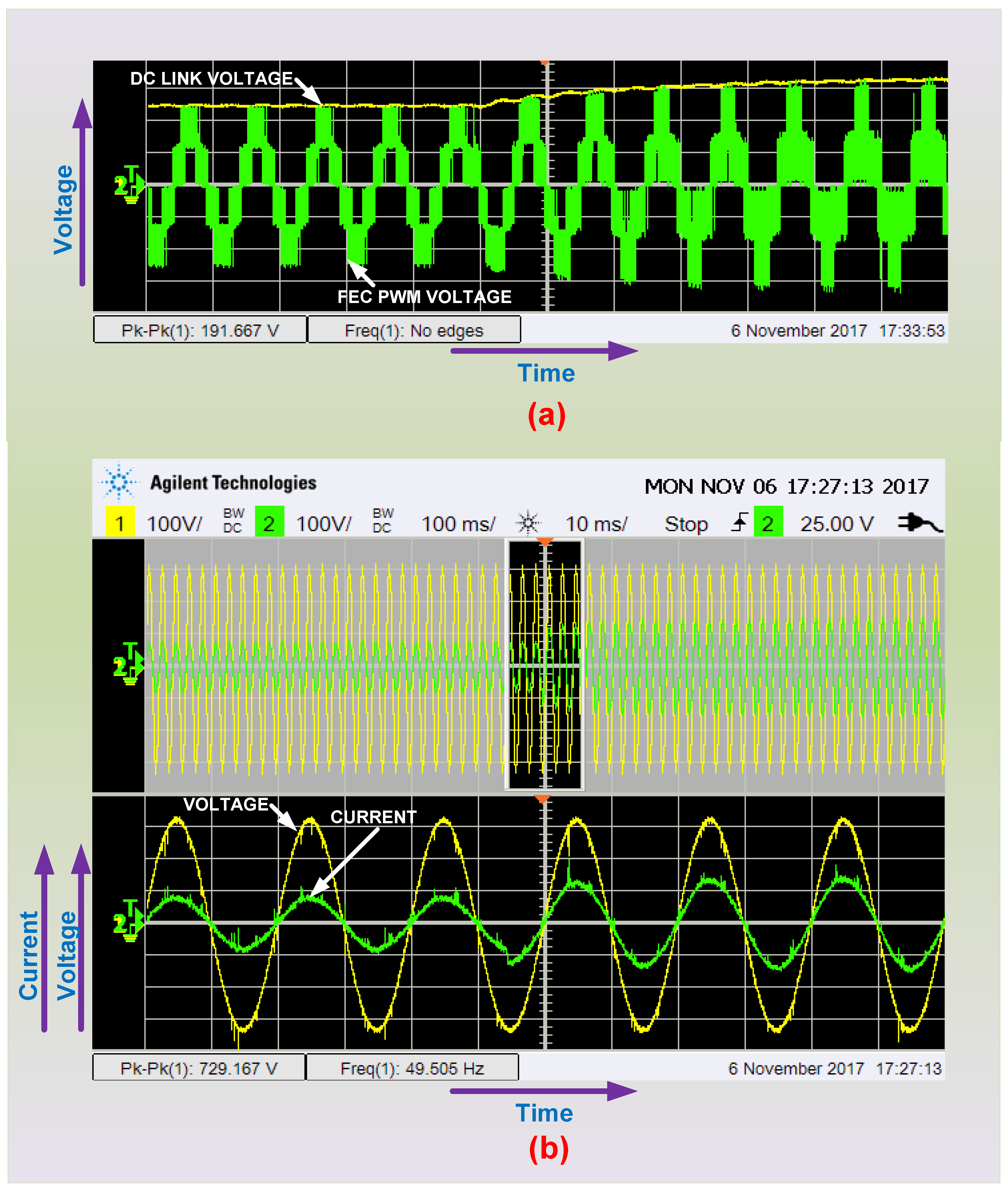
Figure 5.
(a) Input Voltage and Current Waveforms of T-Type Front-End Converter (b) Input Voltage and Current Waveforms of T-Type Front-End Converter during Transition time for a step change in Load.
Figure 5.
(a) Input Voltage and Current Waveforms of T-Type Front-End Converter (b) Input Voltage and Current Waveforms of T-Type Front-End Converter during Transition time for a step change in Load.
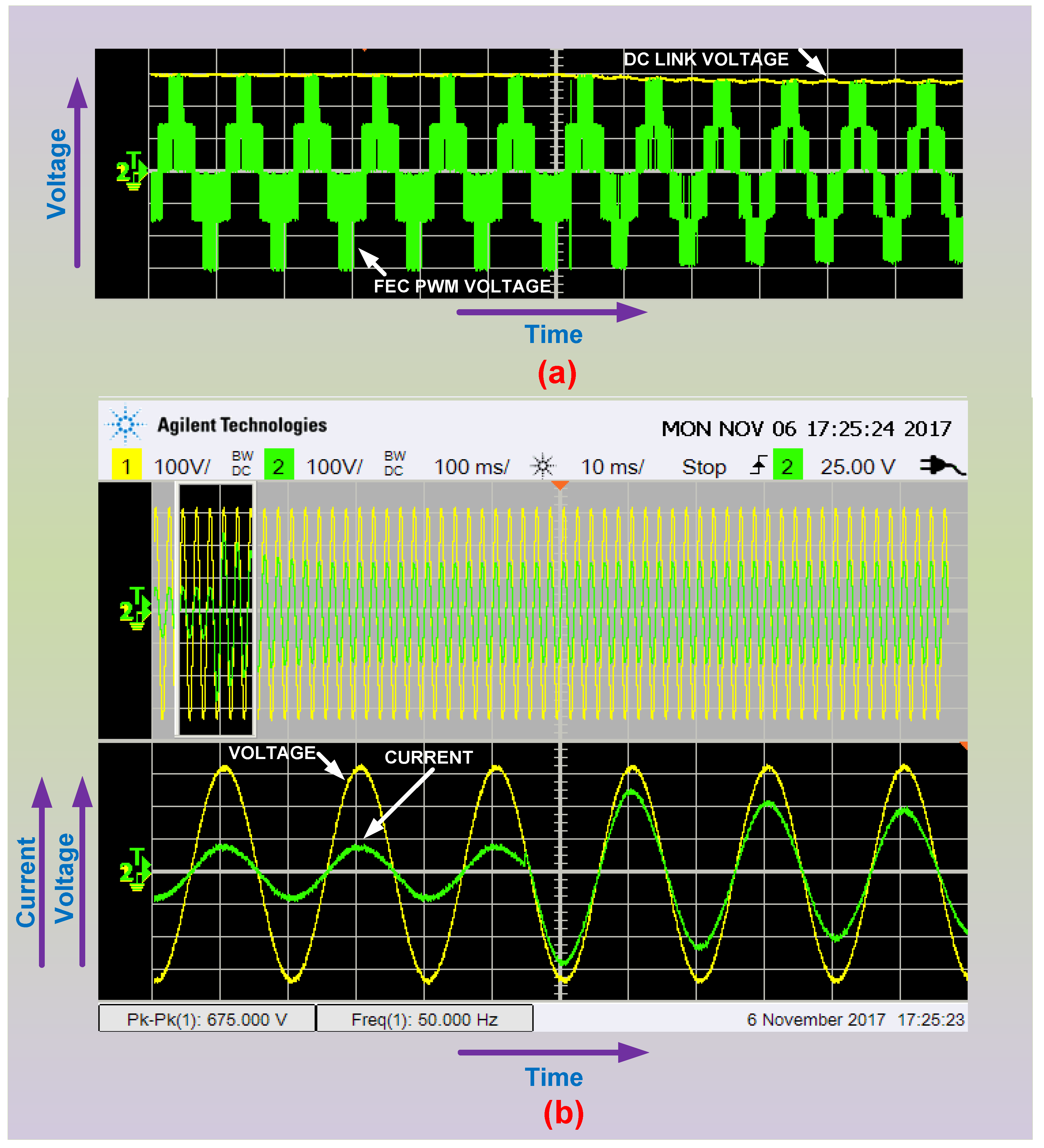
Figure 6.
Control Block diagram of a DC-DC Converter.

Figure 7.
Output Voltage, Current and Powers from an Actual PV array and the PV-simulator for Different Irradiance Values.
Figure 7.
Output Voltage, Current and Powers from an Actual PV array and the PV-simulator for Different Irradiance Values.

Figure 8.
Output Voltage, Current and Powers from an Actual PV array and the PV-Simulator for at an Irradiance of 600 W/Sq.m.
Figure 8.
Output Voltage, Current and Powers from an Actual PV array and the PV-Simulator for at an Irradiance of 600 W/Sq.m.

Figure 9.
Controller-In-Loop Simulation setup for validation of proposed PV-Simulator Controls.
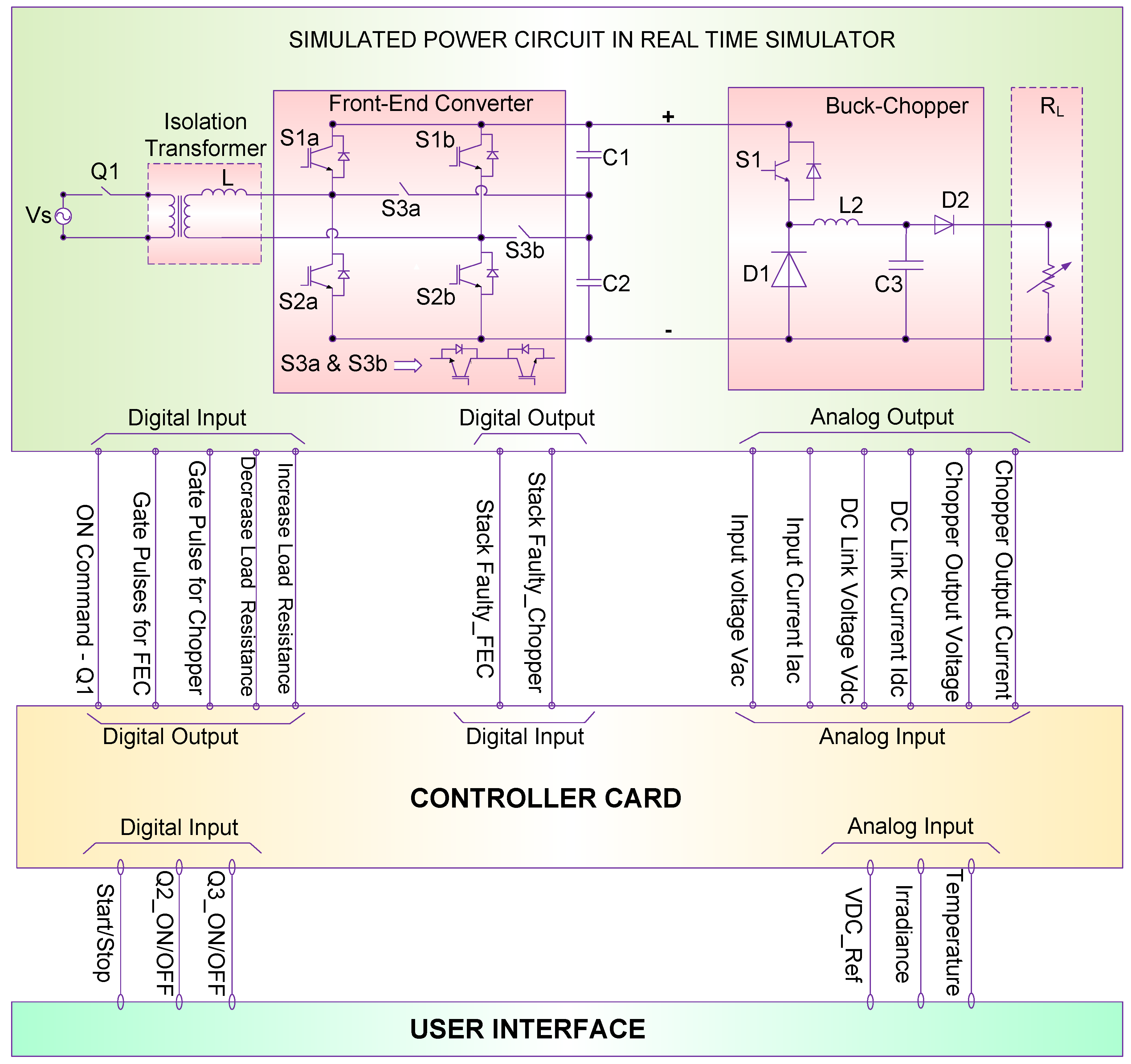
Figure 10.
Output Voltage and Powers of PV-Simulator for Different Irradiance Inputs.

Table 1.
Parameters of Selected PV-array to Be Programmed.
| SL. No. | Reference | Configuration | Remarks |
|---|---|---|---|
| 1 | [3,4] | An LLC resonant DC-DC converter-based PV-simulator | This configuration requires a centre-tapped transformer and two inductors, two IGBT/MOSFET switches, etc. Cost and size of the system increases for higher rated systems due to the higher number of magnetic components. |
| 3 | [5,6] | PV-simulator based on an interleaved buck converter | This configuration requires three inductors and six IGBT/MOSFET switches. The cost of the system is comparatively lesser than [3,4]. |
| 3 | [7] | Buck-boost chopper-based PV-simulator | Cost of this system is comparatively lesser than [3,4,5,6] as this configuration requires two inductors and four IGBT/MOSFET switches. |
| 2 | [8] | Buck chopper-based PV-simulator with two stage LC filter | Two inductors are required at the output side of the chopper. The cost of the system is comparatively lesser than [3,4,5,6,7], but an additional L-C filter stage on the output side is costlier than a buck-chopper-based PV-simulator with a single L-C stage. |
| 2 | [9] | Two quadrant DC-DC converter-based PV-simulator with two stage LC filter | This configuration requires only one inductor on the output stage and two IGBT/MOSFET switches. Hence the cost of this configuration is less that that of the configurations presented in [3,4,5,6,7,8]. |
| 6 | [10,11,12] | Buck chopper-based PV-simulator with two stage LC filter | Buck-chopper-based PV-simulator is cheaper than the systems presented in [3,4,5,6,7,8,9] since this configuration requires only one inductor on the output stage and only one IGBT/MOSFET switch. |
Table 2.
Parameters of Selected PV-Array to Be Programmed.
| SL. No. | Electrical Parameter | Value | Units |
|---|---|---|---|
| PV Module Ratings | |||
| 1 | Module Power (P_Mod) | 435 | W |
| 2 | Open Circuit Voltage (Voc_Mod) | 85.6 | V |
| 3 | Short Circuit Current (Isc_Mod) | 6.43 | A |
| PV Array Ratings | |||
| 4 | No of Series Modules in PV Array (Nse) | 4 | No’s |
| 5 | No of Parallel Modules in PV Array (Np) | 10 | No’s |
| 6 | PV Array Power (P_Mod × Nse × Np) | 17.40 | kW |
| 7 | Maximum DC Voltage (Nse × Voc_Mod) | 342 | V |
| 8 | Maximum Output Current (Np × Isc_Mod) | 64.3 | A |
Table 3.
Details of the Hardware Used in the Controller-In-Loop Simulations.
| SL. No. | Parameter | Description |
|---|---|---|
| Real-Time Simulator | ||
| 1 | Manufacturer | Opal-RT |
| 2 | Processor in Real-Time Simulator | Intel Xeon Quadcore 2.50 GHz |
| 3 | Operating System | QNX |
| 4 | IO Interface | FPGA Based |
| 5 | No of Analog Input Channels | 16 |
| 6 | No of Analog Output Channels | 16 |
| 7 | No of Digital Input Channels | 16 |
| 8 | No of Digital Output Channels | 16 |
| 9 | Analog Channels voltage Range | −10 to +10 V |
| 10 | Digital Channels Voltage range | 0 V = Logic Low, 15 V = High |
| 11 | Front-End Modeling tool | Matlab-Simulink |
| Controller Details | ||
| 12 | DSP Used | TMS320F2812 DSP |
| 13 | No of Analog Input Channels | 16 |
| 14 | No of Digital Input Channels | 16 |
| 15 | No of Digital Output Channels | 16 |
| 16 | No of PWM Outputs | 12 |
| 17 | Analog Channels voltage Range | −10 to +10 V |
| 18 | Digital Channels Voltage range | 0 V = Logic Low, 15 V = High |
Table 4.
Parameters of Programmed PV-Array at Irradiance Inputs of 1000 W/Sq.m and 600 W/Sq.m.
| SL. No. | Electrical Parameter | Value | Units |
|---|---|---|---|
| PV Module Ratings | |||
| 1 | Maximum power of module at 1000 W/Sq.m | 435 | W |
| 2 | Maximum power of module at 600 W/Sq.m | 261 | W |
| 3 | MPP Voltage (Vmpp) at 1000 W/sq.m | 72.9 | V |
| 4 | MPP Current (Impp) at 1000 W/sq.m | 5.97 | A |
| PV Array Ratings | |||
| 5 | No of Series Modules in PV Array (Nse) | 4 | No’s |
| 6 | No of Parallel Modules in PV Array (Np) | 10 | No’s |
| 7 | PV Array Power at 1000 W/sq.m | 17.40 | kW |
| 8 | MPP Current of Array (Impp × Np) at 1000 W/sq.m | 59.7 | A |
| 9 | Maximum PV Array Power at 600 W/sq.m | 10 | kW |
| 10 | MPP Current of Array at 600 W/sq.m | 36 | A |
© 2018 by the authors. Licensee MDPI, Basel, Switzerland. This article is an open access article distributed under the terms and conditions of the Creative Commons Attribution (CC BY) license (http://creativecommons.org/licenses/by/4.0/).
Share and Cite
MDPI and ACS Style
Vavilapalli, S.; Subramaniam, U.; Padmanaban, S.; Blaabjerg, F. Design and Controller-In-Loop Simulations of a Low Cost Two-Stage PV-Simulator. Energies 2018, 11, 2774. https://doi.org/10.3390/en11102774
AMA Style
Vavilapalli S, Subramaniam U, Padmanaban S, Blaabjerg F. Design and Controller-In-Loop Simulations of a Low Cost Two-Stage PV-Simulator. Energies. 2018; 11(10):2774. https://doi.org/10.3390/en11102774
Chicago/Turabian StyleVavilapalli, Sridhar, Umashankar Subramaniam, Sanjeevikumar Padmanaban, and Frede Blaabjerg. 2018. "Design and Controller-In-Loop Simulations of a Low Cost Two-Stage PV-Simulator" Energies 11, no. 10: 2774. https://doi.org/10.3390/en11102774
Note that from the first issue of 2016, this journal uses article numbers instead of page numbers. See further details here.