Article

Switched-Capacitor-Based High Boost DC-DC Converter

1
Department of Telecommunication Operation, Telecommunications University, Nha Trang 650000, Vietnam
2
Department of Electrical Engineering, University of Chosun, Gwangju 61452, Korea
*
Author to whom correspondence should be addressed.
Energies 2018, 11(4), 987; https://doi.org/10.3390/en11040987
Submission received: 22 March 2018 / Revised: 11 April 2018 / Accepted: 17 April 2018 / Published: 19 April 2018
(This article belongs to the Section I: Energy Fundamentals and Conversion)

Abstract

:
A non-isolated high boost DC-DC converter topology based on a switched-capacitor (SC) structure is introduced in this paper. By controlling the duty cycle in each period, the voltage gain of the converter is adjusted. The main features of the proposed SC converter are the continuous input current, achieving high voltage gain with low voltage and current stress on the power components, no use of a high-frequency transformer, and easy to increase the voltage by adding the SC cell. To correct the operating analysis, a 200-W output power prototype was built with the input voltage in the range of [25 V, 50 V] and the output voltage of 200 V. The proposed inverter reaches a maximum efficiency of 93% at the input voltage of 25 V and the output power of 150 W. The simulation and experimental verifications match the analysis.

1. Introduction

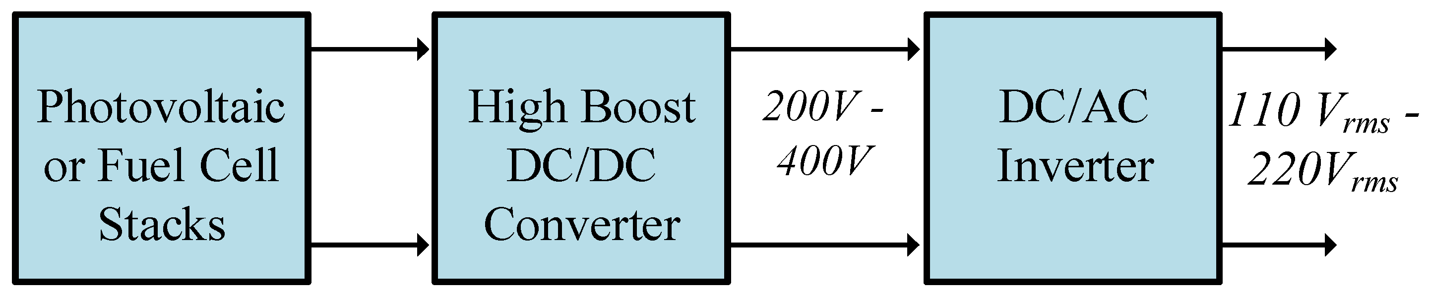
Recently, with the development of industrialization, the use of the renewable resources—photovoltaic arrays, fuel cells, etc.—have been a most effective solution. However, they are DC sources with low voltage, low current, and instability. To link them to loads or grid applications, the power conversion generation in Figure 1 was developed. To convert the low voltage of the renewable sources into 200 V or 400 V DC voltage, a high step-up DC-DC stage [1,2,3] is set up as the first stage in the power-conversion system. The second-stage DC-AC converter can provide 110 Vrms or 220 Vrms AC volts for the grid-connected application.
Since the components have an equivalent series resistance (ESR), the traditional boost converter is difficult to step up a large gain voltage. When the high boost voltage is required, the boost converter needs to have a large duty cycle, which leads to high conduction loss and reducing efficiency [4,5,6]. Moreover, in order to achieve the high boost voltage gain, the various DC-DC converters have been presented, including isolated and non-isolated topologies. The isolated topology [7,8,9,10] can provide the isolation between input and output terminals, which is based on a high-frequency transformer. Since the isolated topologies include a DC-AC stage and an AC-DC stage, they required a number of components, which increase the circuit’s size. If the leakage inductances are designed carelessly, the switches appear as a voltage spike. The non-isolated topologies [11,12,13,14,15,16,17,18,19] can achieve a high efficiency with a simple circuit because of the lack of a transformer. In the non-isolated topologies, the high step-up voltage gain can be achieved by using the following techniques: cascade boost, switched-capacitor, switched-inductor, coupled inductor, and a mixture of them. The coupled-inductor-based converters [12,13,14] have a large voltage conversion ratio with increasing efficiency and reduces the voltage/current stress on switches and diodes. However, the circuits are complex to design and the leakage problem of the coupled inductor causes a high voltage spike on semiconductor components. The dual-switch-based converters [15,16,17] present a high voltage gain with high input current ripple. In these topologies, an additional active switch is required with the increasing gate drive. The SC structure was proposed in [18]. By charging the capacitors in parallel and discharging them in series the SC-based converter produces a high voltage at the output side. In [19], an interleaved DC-DC multilevel converter was proposed by combining a multilevel boost structure and a single inductor multiplier Cuk converter to achieve a minimum input current ripple. A non-isolated high step-up DC-DC converter with single-inductor-energy-storage cell-based SCs (SIESC-SCs) was introduced in [20]. By changing the SC cell connection, various converter topologies are obtained.
To decrease the converter’s size and obtain a high voltage gain, the cascade boost converter, the voltage multiplier cells (VMC) boost converter, and the dual boost converter were proposed, as shown in Figure 2. The cascade boost converter, as shown in Figure 2a, can provide a high ratio, but the circuit is complex, and the size and cost of the converter are increased. The cascade converter can reduce switch S1 and diode D1 voltage stress, high flexibility, and suitability for high power applications. However, the switch S2 and diode D2 voltage stress are high. The VMC boost converter were presented in [5] and is shown in Figure 2b. The voltage ratio of the VMC boost converter can achieve a larger gain voltage by increasing the N cell of the VMC. The switches’ and diodes’ voltage stresses are decreased, and the diodes are turned off with ZCS. However, the duty cycle is limited and the switches’ current stress is large, and the voltage stress is dependent on the number of VMC. The dual converter was quoted from [6], as shown in Figure 2c. Similarly, the dual boost converter decreases the voltage stress on the switches, the inductor current is rated roughly at half of the total input current, and the isolated gate driver is needed for the dual boost converter.
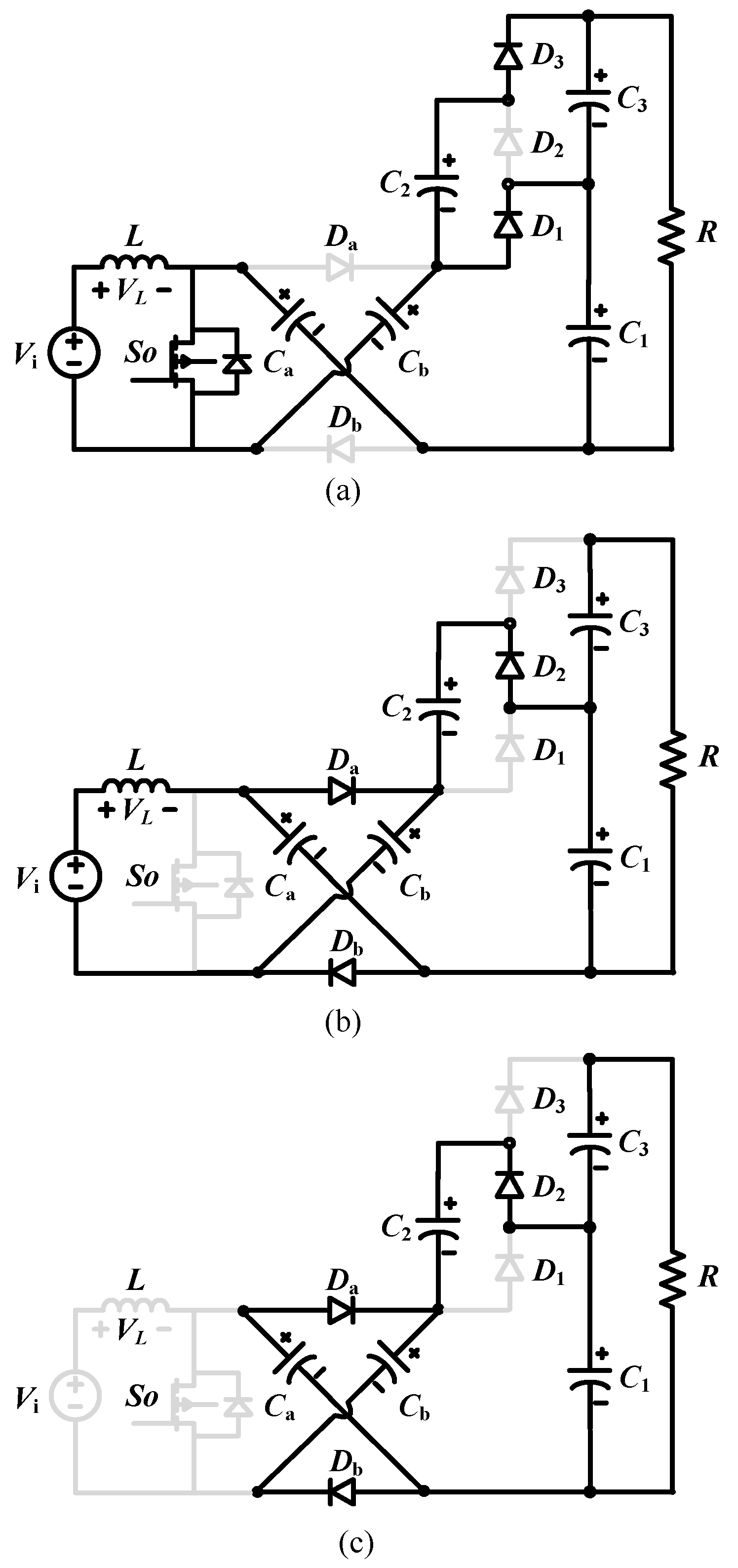
This paper proposes a new boost converter based on a switched-capacitor structure. The proposed SC converter has a large step-up gain with continuous input current. The operating principles and circuit analysis in continuous conduction mode (CCM) and discontinuous mode (DCM) are presented. The parameters selection of the proposed SC converter and a comparison with conventional converters are shown. Simulation and experiment verifications prove the correctness of the operating analysis.

2. Proposed SC Converter Topology

2.1. Proposed Topology

The proposed SC non-isolated boost DC-DC converter is presented in Figure 3, which includes a SC structure and multilevel-boost converter. It uses a single switch, five diodes, single inductor, five capacitors and load. Figure 4 shows a detailed PWM algorithm for the proposed SC converter. The switch S0 is controlled by comparing the reference voltage, Vref to the triangle waveform with the amplitude of “1”.

2.2. Circuit in CCM Operation

To facilitate the circuit analysis of the proposed converter, the following conditions are guaranteed as all components seem ideal and reflect no losses, the voltage of capacitors is constant, and the inductor current is increased and decreased linearly.
Mode 1 [t0–t1, Figure 5a]: The time interval in this mode is DT, where D is the duty cycle of switch S0 in one switching period T. The MOSFET S0 is turned on. The diodes D1 and D3 are forward-biased. The inductor is charged. We have the equivalent equations:
{ V L = V i V C 1 = V C a + V C b V C 2 = V C 3
Mode 2 [t1–t2, Figure 5b]: This interval time in mode 2 is (1 − D)T. Switch S0 is turned off. The diodes Da, Db, and D2 are forward-biased. The inductor delivers the stored energy to the load. We have:
{ V L = V i V C a V C a = V C b V O = V C 1 + V C 3
The average voltage across the inductor in period switching is zero:
V ¯ L = D V i + ( 1 D ) ( V i V C a ) = 0
In the steady state, the capacitor voltage and output voltage are calculated as:
{ V C = V C a = V C b = V C 2 = V C 3 = 1 1 D V i V C 1 = 2 V C = 2 1 D V i V O = 3 V C = 3 1 D V i

2.3. Circuit in DCM Operation

When the power load is reduced to a light load, the converter works in CCM. Then, the inductor current goes to zero and stays there until the new switching period starts. The inductor current waveform is the last one sketched in Figure 4. The inverter has one more mode, as shown in Figure 5c.
Mode 1 [t0–t1, Figure 5a] and mode 2 [t1–tx, Figure 5b]: These modes are the same as modes 1 and 2 in the CCM. The interval time in modes 1 and 2 is DT and (1 − DDx)T, respectively.
Mode 3 [tx–t2, Figure 5c]: The interval time in this mode is DxT. The switch S0 is still off. The inductor current is zero. The equivalent circuit is shown in Figure 5c. The switching ripple of peak amplitude is:
Δ I L = V i L D T
If the power losses of circuit are equal to zero, the average input current is calculated as:
I ¯ i = P o V i = V o 2 R V i = 9 V i ( 1 D ) 2 R
where Po and R are the power and the resistance of the load, respectively.
The condition of the proposed converter in the discontinuous conduction mode is:
I ¯ L < ( Δ I L / 2 )
Substituting Equations (5) and (6) into (7), we have:
K < K c r i t ( D )
where K = 18 L / ( R T ) , and K c r i t ( D ) = D ( 1 D ) 2 .
Applying the inductor volt-second balance, the Dx was obtained as:
D x = D V i V C V i
From Figure 5, the average inductor current is easily evaluated:
I ¯ L = V i 2 L D ( D + D x ) T = V o 2 V i R
From Equations (8)–(10), we have:
G D C M = V o V i = 3 + 9 + 36 D 2 K 2
Figure 6a gives the voltage gain of the proposed SC converter in DCM/CCM. The output voltage gain in the DCM is higher in the CCM. The converter works in the CCM when Kcrit > 0.148. Figure 6b shows the relationship between Kcrit and D at CCM/DCM boundary.

3. Capacitance and Inductance Selections

3.1. Inductance Selection

The inductor is chosen based on the current ripple through it. From Figure 5a, we have:
V L = L d i d t = V i
where di/dt is the variation of the inductor current. Equation (12) can be rewritten as:
V L = L Δ i Δ t = V i
The inductor current ripple is calculated as:
Δ i = a % I L = H P V i
where H (%) and a% are the converter efficiency and the inductor current ripple, respectively.
Based on the inductor current ripple in DT interval and Equations (13) and (14), the inductance is calculated as:
L = V i 2 a H P o D T

3.2. Capacitance Selection

In mode 2, the peak current flows to capacitor C3 calculated as:
I C 3 = C 3 d v d t = I o
The capacitance is chosen as C = Ca = Cb = C2 = C3 = 0.5C1. From Equation (16), we obtain:
C = 3 D T % b R
where %b is the capacitor C3 voltage ripple.

3.3. Calculation of Power Loss

Power Loss of Switch:
The power loss of switch are the conduction loss and the switching loss. The MOSFET conduction loss of switch S0 is:
P c S = R D S o n D I i n 2 / 4
where RDSon is the drain-source resistance of the MOSFET.
The MOSFET switching loss is determined as [21]:
P s w S = V C I i n 2 f s ( t r u + t f i 2 + t r i + t f u 2 )
where tru, tfu, tri, and tfi are the rising time, falling time of voltage, rising time, and falling time of current, respectively, and the parameters are obtained from the datasheet.
Power Loss of the Diodes:
The conduction loss of diodes D0, D1, and D2 is:
P C D = 2 [ u D x I i n / 2 + R D x I i n 2 / 4 ] ( 1 D ) + 2 ( u D x I o / 2 + R D x I o 2 / 4 ) D + ( u D x I o / 2 + R D x I o 2 / 4 ) ( 1 D )
where uDx and RDx are the drop voltage and the resistance of the Da, Db, D1D3, respectively.
The reverse recovery loss of the diodes is:
P r r D = 5 Q r r f V C f s
where Qrrf is the reverse recovery charge of diodes.
Power Loss in the Capacitor:
The capacitor power loss is calculated by:
P C = r C a I C a 2 + r C b I C b 2 + r C 1 I C 1 2 + r C 2 I C 2 2 + r C 3 I C 3 2
where rCa, rCb, rC1, rC2, and rC3 are the internal resistances of C1, C2, and C3 capacitors.
The current of capacitors Ca, Cb, C1, C2, and C3 are defined by:
{ I C a = I C b = I i n 2 I C 1 = ( I o I i n / 2 ) 2 D + ( I o 2 ) 2 ( 1 D ) I C 2 = I o 2 I C 3 = ( I o 2 ) 2 D + I o 2 ( 1 D )
Power Loss of the Inductor:
The power loss of the inductor is such as the loss of core and copper wire. The inductor core loss is expressed as:
P f e = K f e Δ B β A c l m
where Kfe is a constant, β is selected from the core datasheet; Ac is the core cross-sectional area; and lm is the core mean magnetic path length.
The inductor copper losses are given by:
P c u = R L I L _ R M S 2
where RL is the resistance wire.
The power loss is calculated and shown in Figure 7a at Vi = 25 V, Vo = 200 V and Po = 200 W. The parameters of device are used to calculate the power loss, are shown in Table 1 and Table 2. The total power loss is 13.55 W and the calculated efficiency of the proposed SC converter is 93.23%. Figure 7b shown the calculated efficiency comparison between the proposed converter and SIESC-SCs [20] when Vi = 25 V and Vo = 200 V. The power loss of both proposed converter and SIESC-SCs are determined based on the parameters in Table 2. As shown in Figure 7b, the calculated efficiency of the proposed SC converter is slightly lower than that of the SIESC-SCs [20]. This is because the proposed inverter uses two more diodes and capacitors to obtain the high voltage gain. As shown in Figure 7a, the major loss contributions are from diodes and capacitors. Note that the parameters for power loss calculation in Table 2 are chosen from devices those are available in the laboratory for the experimental test. Therefore, these parameters are not optimally selected for efficiency consideration. The devices including MOSFET and diodes with lower voltage rating should be selected to reduce the power loss of the proposed converter.

4. Comparison with Other High Voltage Gain Converters

The comparison between the proposed SC converter and other converters, including the dual boost converter (DBC) [3], the cascade boost converter (CBC) [5], the boost voltage multiplier cell (B-VMC) (n = 2) [6], the single inductor multiplier Cuk converter (SLMC) [19], and the converter with the SIESC-SCs [20], are shown in Table 3 and Table 4. In the comparison to DBC [3], B-VMC [6], and CBC [5], the proposed SC converter saves one inductor. Moreover, the voltage stress on diodes and switches of the proposed SC converter is small. Similar to the CBC [5] and B-VMC [6], the proposed SC converter uses one active switch. Compared to the DBC [3], B-VMC [6], CBC [5], and SIESC-SCs [20], the proposed SC converter uses two more diodes and capacitors, but the voltage gain of the proposed SC converter is higher. When the gain and voltage stress of active components are considered, the SLMC [19] is an interesting topology. However, the proposed SC converter has the same advantages with SLMC [19] and uses one less capacitor and one less diode.
Figure 8 shows the voltage gain comparison between the proposed SC converter and the other non-isolated converters in the CCM. The voltage gain of the proposed SC converter is the same as that of SLMC [19] and is highest when D < 2/3. Therefore, the proposed configuration is more profitable than other non-isolated configurations of the boost coefficient.

5. Simulation and Experimental Verifications

5.1. Simulation Verification

To confirm the operating principle of the proposed DC-DC converter, PSIM simulation software was used to prove the correctly of the operating principle with the parameters as L = 0.4 mH, C1 = 470 µF, Ca = Cb = C2 = C3 = 220 µF. The on-resistance of the MOSFET is 24 mΩ. The forward-voltage of diodes is set to 1.4 V. The switching frequency of semiconductor components is 20 kHz. The input DC source is used to adjust from 25 V to 50 V. The output voltage is stepped up to 200 V.
Figure 9a shows the simulation results for the proposed SC converter when Vi = 25 V and D = 0.644. As shown in Figure 9a, the input current is continuous and the peak-to-peak inductor current is 1.96 A. The capacitor voltages are boosted to VCa = VCb = 68 V, VC1 = 134 V, and VC2 = VC3 = 66 V. Then, the input voltage is increased to 50 V and the duty cycle is decreased to 0.282, while the output voltage is still 200 V, as shown in Figure 9b. The input current in this case is also continuous with the peak-to-peak inductor current of 1.7 A.

5.2. Experimental Verifications

The experiment results are implemented by using a TMS320F28335 DSP kit with experimental parameters as shown in Table 5 and Table 6. One MOSFET is STW88N65M5 and five diodes are DSEI30-06A. The output voltage and output powers are 214 V and 200 W, respectively. Figure 10 shows a photograph of the converter prototype.
Figure 11 shows the experimental results of the proposed SC converter in CCM when Vi = 25 V. The output voltage is boosted to 200 V when the input voltage is 25 V. The peak-to-peak ripple input current is 2 A, which is close to the simulation value.
Figure 12 shows the measured efficiency of the proposed SC converter when the output power is changed from 80 W to 200 W. The WT230 digital power meter is set up to connect the input and output. The maximum measured efficiency is 93% at 150 W. The efficiency for the experiment can be improved with the optimal selection of components. The experimental results are slightly similar from the theoretical and simulation results.
Figure 13 shows the voltage gain between the calculated values and simulated values. The simulated values are slightly lower than the calculated values because the parasitics on the devices were set in the simulation.

6. Conclusions

A non-isolated boost DC-DC converter was proposed in this paper. The major advantages of the proposed SC converter are as follows: high voltage gain; decrease voltage and current stress on the power device, which helps reduce the loss; and being easy to increase the voltage gain and control using one switch. The operating principles in the CCM and DCM, parameters design, power loss analyses, and the comparison with the other non-isolated high boost converters are discussed. The experimental results of the proposed converter at 25 V input voltage are presented to produce the output voltage of 200 V. The maximum measured efficiency of the converter is 93% at 150 W. The experimental and simulation verifications were shown to verify the theoretical analysis.

Acknowledgments

This work was supported by the Korea Institute of Energy Technology Evaluation and Planning (KETEP) and the Ministry of Trade, Industry and Energy (MOTIE) of the Republic of Korea (no. 20164010201020).

Author Contributions

Van-Thuan Tran and Minh-Khai Nguyen conceived and designed the experiments; Van-Thuan Tran performed the experiments; Minh-Khai Nguyen and Youn-Ok Choi analyzed the data; Van-Thuan Tran and Geum-Bae Cho wrote the paper; Minh-Khai Nguyen revised the paper.

Conflicts of Interest

The authors declare no conflict of interest.

Nomenclature

B-VMCBoost voltage multiplier cell
CBCCascade boost converter
CCMContinuous conduction mode
DDuty cycle
DBCDual boost converter
DCMDiscontinuous conduction mode
ESREquivalent series resistance
PWMPulse width modulation
SCSwitched-capacitor
SCsSwitched-capacitor based
SIESCSingle-inductor-energy-storage cell-based
SLMCSingle inductor multiplier Cuk converter
TPeriod time
VMCVoltage multiplier cells
ZCSZero current switching

References

  1. Toffoli, F.L.; Pereira, D.C.; Paula, W.J.; Junior, D.S.O. Survey on non-isolated high-voltage step-up DC–DC topologies based on the boost converter. IET Power Electron. 2015, 8, 2044–2057. [Google Scholar] [CrossRef]
  2. Nymand, M.; Andersen, M.A.E. High-efficiency isolated boost DC–DC converter for high-power low-voltage fuel-cell applications. IEEE Trans. Ind. Electron. 2010, 57, 505–514. [Google Scholar] [CrossRef]
  3. Jin, K.; Yang, M.; Ruan, X.; Xu, M. Three-level bidirectional converter for fuel-cell/battery hybrid power system. IEEE Trans. Ind. Electron. 2010, 57, 1976–1986. [Google Scholar] [CrossRef]
  4. Li, W.; He, X. Review of nonisolated high-step-up DC/DC converters in photovoltaic grid-connected applications. IEEE Trans. Ind. Electron. 2011, 58, 1239–1250. [Google Scholar] [CrossRef]
  5. Bratcu, A.I.; Munteanu, I.; Bacha, S.; Picault, D.; Raison, B. Cascaded DC–DC converter photovoltaic systems: power optimization issues. IEEE Trans. Ind. Electron. 2011, 58, 403–411. [Google Scholar] [CrossRef]
  6. Garcia, F.S.; Pomilio, J.A.; Spiazzi, G. Modeling and control design of the interleaved double dual boost converter. IEEE Trans. Ind. Electron. 2013, 60, 3283–3290. [Google Scholar] [CrossRef]
  7. Nguyen, M.K.; Lim, L.C.; Choi, J.H.; Cho, G.B. Isolated High Step-up DC-DC Converter Based on Quasi-Switched-Boost Network. IEEE Trans. Ind. Electron. 2016, 63, 7553–7562. [Google Scholar] [CrossRef]
  8. Ouyang, Z.; Sen, G.; Thomsen, O.C.; Andersen, M.A.E. Analysis and design of fully integrated planar magnetics for primary–parallel isolated boost converter. IEEE Trans. Ind. Electron. 2013, 60, 494–508. [Google Scholar] [CrossRef] [Green Version]
  9. Nguyen, M.K.; Duong, T.D.; Lim, L.C.; Kim, Y.J. Isolated boost DC–DC converter with three switches. IEEE Trans. Power Electron. 2018, 33, 1389–1398. [Google Scholar] [CrossRef]
  10. Shi, X.; Jiang, J.; Guo, X. An efficiency-optimized isolated bidirectional DC-DC converter with extended power range for energy storage systems in microgrids. Energies 2013, 6, 27–44. [Google Scholar] [CrossRef]
  11. Prudente, M.; Pfitscher, L.L.; Emmendoerfer, G.; Romaneli, E.F.; Gules, R. Voltage multiplier cells applied to non-isolated DC-DC converters. IEEE Trans. Power Electron. 2008, 23, 871–887. [Google Scholar] [CrossRef]
  12. Hsieh, Y.P.; Chen, J.F.; Yang, L.S.; Wu, C.Y.; Liu, W.S. High-conversion-ratio bidirectional DC/DC converter with couple inductor. IEEE Trans. Ind. Electron. 2014, 61, 1311–1319. [Google Scholar] [CrossRef]
  13. Tang, Y.; Fu, D.; Kan, J.; Wang, T. Dual switches DC/DC converter with three-winding-coupled inductor and charge pump. IEEE Trans. Power Electron. 2016, 31, 461–469. [Google Scholar] [CrossRef]
  14. Padmanaban, S.; Bhaskar, M.S.; Maroti, P.K.; Blaabjerg, F.; Fedák, V. An original transformer and switched-capacitor (T & SC)-based extension for DC-DC boost converter for high-voltage/low-current renewable energy applications: hardware implementation of a new T & SC boost converter. Energies 2018, 11, 783. [Google Scholar] [CrossRef]
  15. Tang, Y.; Wang, T.; Fu, D. Multicell switched-inductor/switched-capacitor combined active-network converters. IEEE Trans. Power Electron. 2015, 30, 2063–2072. [Google Scholar] [CrossRef]
  16. Yang, L.S.; Liang, T.J.; Chen, J.F. Transformerless DC-DC converters with step-up voltage gain. IEEE Trans. Ind. Electron. 2009, 56, 3144–3152. [Google Scholar] [CrossRef]
  17. Nguyen, M.K.; Duong, T.D.; Lim, L.C. Switched-capacitor-based dual-switch high-boost DC–DC converter. IEEE Trans. Power Electron. 2018, 33, 4181–4189. [Google Scholar] [CrossRef]
  18. Axelrod, B.; Berkovich, Y.; Ioinovici, A. Switched-capacitor/switched-inductor structures for getting transformerless hybrid DC-DC PWM converters. IEEE Trans. Circuits Syst. I 2008, 55, 687–696. [Google Scholar] [CrossRef]
  19. Hernandez, C.A.V.; Maldonado, J.C.M.; Resendiz, J.E.V.; Caro, J.C.R. Modeling and control of an interleaved DC-DC multilevel boost converter. In Proceedings of the IEEE 18th Workshop on Control and Modeling for Power Electronic (COMPEL), Stanford, CA, USA, 9–12 July 2017; pp. 1–6. [Google Scholar] [CrossRef]
  20. Wu, G.; Ruan, X.; Ye, Z. Nonisolated high step-up DC-DC converters adopting switched-capacitor cell. IEEE Trans. Ind. Electron. 2015, 62, 383–393. [Google Scholar] [CrossRef]
  21. Graovac, D.; Pürschel, M.; Kiep, A. MOSFET power losses calculation using the datasheet parameters. Infineon Appl. Note 2006, 1, 1–23. [Google Scholar]
Figure 1. Power-conversion system.
Energies 11 00987 g001
Figure 2. Conventional boost converter topologies. (a) The cascade boost topology; (b) the boost topology with voltage multiplier cells (VMC); and (c) dual boost converter.
Energies 11 00987 g002aEnergies 11 00987 g002b
Figure 3. Proposed SC boost DC-DC.
Energies 11 00987 g003
Figure 4. Key waveforms of the proposed SC DC-DC converter.
Energies 11 00987 g004
Figure 5. The operating mode of the proposed converter: (a) S0 on; (b) S0 off; and (c) the circuit in DCM.
Energies 11 00987 g005
Figure 6. Curves in DCM/CCM operation. (a) Voltage gain of the proposed SC converter in DCM/CCM; (b) Kcrit and D at the CCM/DCM boundary.
Energies 11 00987 g006
Figure 7. Power loss calculation. (a) Power loss of the proposed SC converter; and (b) comparison of the calculated efficiency.
Energies 11 00987 g007
Figure 8. Voltage gain comparison with other non-isolated converters.
Energies 11 00987 g008
Figure 9. Simulation waveforms when (a) Vi = 25 V and (b) Vi = 50 V. Waveforms: input voltage, output voltage, capacitor C1, C2, C3, Ca and Cb voltages, input current, drain-source voltage of S0, and diode Da and D1 voltages.
Energies 11 00987 g009
Figure 10. Prototype of the converter.
Energies 11 00987 g010
Figure 11. Experimental results when Vi = 25 V and D = 0.65. From top to bottom: (a) input current and output voltage; (b) drain-source current and voltage of switch S0; and (c,d) all diodes’ voltage.
Energies 11 00987 g011aEnergies 11 00987 g011b
Figure 12. Converter efficiency with different output powers.
Energies 11 00987 g012
Figure 13. Voltage gain comparison between calculation and simulation.
Energies 11 00987 g013
Table 1. Conducting current of the devices in the proposed SC converter.
DevicesConducting CurrentConducting Time
SoIL/2D·T
Da, DbIL/2(1 − DT
D1, D3Io/2D·T
D2Io/2(1 − DT
LILT
Ca, CbIL/2T
C1IoIL/2D·T
Io/2(1 − DT
C2Io/2T
C3Io/2D·T
Io(1 − DT
Table 2. Parameters of the devices.
DevicesSIESC-SCs [20]Proposed SC Converter
MOSFET S0STW88N65M5 (650 V, 84 A, 24 m Ω)
DiodesDSEI30-06A (600 V, 37 A)DSEI30-06A (600 V, 37 A)
ESR of capacitors280 mΩ280 mΩ
ESR of C1 (470 µF/400 VDC)130 mΩ130 mΩ
Inductor coreCM777125 (142 nH/N2)CM777125 (142 nH/N2)
Copper wire resistivity (ρ)1.724 µΩ-cm1.724 µΩ-cm
Table 3. Comparison of topologies.
ConverterLCSwitchesDiodes
DBC [3]2222
B-VMC (n = 2) [6]2313
CBC [5]2212
SLMC [19]1616
SIESC-SCs [20]1313
Proposed1515
Table 4. Comparison voltage stress and gain of topologies.
ConverterSwitched StressDiode StressVoltage Gain
DBC [3]Vo/2Vo/2G = (1 + D)/(1 − D)
B-VMC (n = 2) [6]Vo/2Vo/2G = 2/(1 − D)
CBC [5]Vo/2Vo/2G = 1/(1 − D)2
SLMC [19]Vo/3Vo/33/(1 − D)
SIESC-SCs [20]Vo/2Vo/22/(1 − D)
ProposedVo/3Vo/3G = 3/(1 − D)
Table 5. Parameters for verification.
ParameterValues
Output power, Po200 W
Input voltage, Vi25 V
Output voltage, Vo200 V
Switching frequency20 Khz
The ripple of inductor current (a%)≤20%
The ripple of capacitor voltage (b%)≤5%
Table 6. Accessories used for experiments.
NumberComponentValues
1Inductor L0.4 mH; 20 A
2Capacitor Ca, Cb, C2, C3220 µF; 400 V
3Capacitor C1470 µF; 400 V
4Diode Da, Db, D1, D2, D3DSEI30-06A
5Mosfet S0STW88N65M5
6Load (R)200 Ω

