Abstract
This paper presents the design and implementation of a digital control system for modular multilevel converters (MMC) and its use in a 5 kW small-scale prototype. To achieve higher system control reliability and multi-functionality, the proposed architecture has been built with an effective split of the control tasks between a master controller and six slave controllers, one for each of the six arms of the converter. The MMC prototype has been used for testing both converter and system-level controls in a reduced-scale laboratory set up of a Multi-Terminal DC transmission network (MTDC). The whole control has been tested to validate the proposed control strategies. The tests performed at system level allowed exploration of the advantages of using an MMC in a MTDC system.
1. Introduction
Due to the energy challenges the world is facing today, the interest in the integration into the utility grids of renewable energy sources has significantly increased in recent years. In this context, high voltage direct current (HVDC) systems are considered one of the best options to achieve high reliability in future long-distance offshore grids that are needed to interconnect offshore wind farms, loads and large-scale storage facilities [1].
Among the different power converter topologies proposed in the literature on HVDC applications, Modular Multilevel Converters (MMC) [2] have emerged in recent years due to their attractive properties such as low harmonic distortion, scalability and flexibility. The use of MMC for HVDC systems has been largely studied by the scientific community and some commercials products have been developed by constructors such as ABB, Siemens and Alstom [3,4].
HVDC systems using MMC installed in the last decade are mostly point-to-point systems [5,6,7]. However, the needs to strengthen the existing AC transmission grids and to balance the intermittent power of offshore wind farms over a wider area by interconnecting multiple neighboring HVDC systems have increased the interest on Multi-terminal HVDC systems (MTDC) [8,9]. The use of MMC in MTDC systems instead of conventional two-level voltage source converters (VSC) has the already cited advantages of being redundant and scalable, to reduce or eliminate bulky harmonics filters on the AC side and to avoid DC link capacitors banks. Despite these advantages, many technical challenges must be tackled to allow their large-scale use. Among these challenges, the lack of a standardized grid code for interconnecting adjacent HVDC systems [10], the DC faults protection management [11,12], the experimental validation of system control strategies to ensure power flow and DC voltage control can be cited.
Concerning this last issue, MMC-based MTDC system control can be split among a high-level (or system-level) control and a low-level (or converter-level) control [13,14,15,16,17,18]. To test and verify these control levels under realistic conditions, as well as their interactions, it is useful to make use of small-scale laboratory prototypes, able to handle the various operational modes. Some small-scale prototypes have been proposed in the scientific literature since the introduction of MMC. For instance, a prototype of MMC is built in [19], with 44 submodules (SM) per arm, each SM capacitor with a nominal voltage at 10 V. In [20], a 20 kW back-to-back MMC-based system with 3 SM per arm is presented, while [21] presents a 25 kW six-level MMC prototype. In [22], a hybrid small-scale prototype is proposed for Alternate Arm Converter (AAC) and MMC.
Considering all these previous studies, it is obvious that, given the large number of submodules used to form the whole structure of an MMC [6], the complex command and control schemes require efficient architectures. This can only be implemented by digital control techniques, making use of advanced FPGA (Field Programmable Gate Array) or DSP (Digital Signal Processors) for fast calculation and accurate timing of the switching signals of the multiple power semiconductors. An FPGA-based control of an MMC has been proposed in [23], making use of a lookup table for the generation of the output references. This approach is not well suited for closed loop control of both the external and internal dynamic behavior of the MMC. it is obvious that a single microcontroller will have difficulties in effectively performing the complex control schemes and the communication with external peripherals. Most of previous works propose a combination of DSP and FPGA boards to handle the control and communication. In [24], the combination of both processors (DSP and FPGA) is used as a central supervision unit. The DSP performs the analog to digital conversion and all the high-level control tasks, while the FPGA manages the modulation, the capacitor voltage balancing and the communication with the submodules tasks. This allows the obtaining of the advantage of a central modulator, which generates all naturally synchronized PWM signals for all switches. However, the capacitor voltage balancing in an MMC usually uses a sorting algorithm which is in itself a sequential process, not leading to an efficient use of parallel logical resources.
Distributed controller architecture can meet these challenges. A distributed architecture fits very well with the scalability of the converter’s structure and the computational load is shared between several microprocessors. Nevertheless, a distributed architecture of the controller requires an effective synchronization of all arm controllers to ensure that the gate signals of all submodules are synchronous. A robust and fast communication link between the master controller and arm controllers must also be assured.
In this paper, a small-scale MMC prototype with a controller architecture designed with only DSPs is presented. The master controller uses a dual core processor which combines a C2000 Texas Instruments (TI) MCU for real time control tasks and an Arm Cortex-M3 processor for the communication purposes. This master controller interacts with six slave controllers, one for each arm, implemented with another C2000 Texas Instruments MCU. This MMC prototype is used in a reduced-scale laboratory setup of a MTDC [25] to implement both system-level and converter-level controls, and to study MMC interactions with other VSC in an existing MTDC system.
Novelty of the paper concerns the experimental verification of the usefulness of the proposed MMC control structure to ensure power flow and DC voltage control in MTDC systems. Testing on a reduced-scale mock-up is, in the opinion of the authors, a step further in comparison to the various HIL (Hardware In a Loop) real-time simulation systems options available on the market. Moreover, it will give to the reader a deep description of several implementation details, concerning both hardware and software choices made.
The paper is organized as follows: Section 2 presents the topology of MMC and a brief review of its control and MTDC control strategies. Section 3 describes the controller structure, the task partitioning as well as the communication protocols. The actual implementation and the experimental validation of the proposed architecture are presented in Section 4. A discussion on how this architecture may be practically extended to be used in MMC systems utilizing more submodules is done in Section 5. Finally, conclusion is given in Section 6.
2. Structure of MMC and Control Strategies
2.1. Structure
Figure 1 presents the typical structure of an MMC converter [1]. It consists of six arms, working as voltage sources. Each arm is made of N power submodules. A submodule consists of a storage capacitor and a half or full bridge converter. The bridge is used to insert or bypass the capacitor. The three-phase AC voltages and the total arm voltage are respectively composed of 2N + 1 and N + 1 levels per signal cycle, corresponding to different insertions or removal of capacitors. This minimizes voltage harmonic distortions and consequently allows reduction/elimination of the filter on the AC side. Furthermore, a large and bulky capacitor on the DC side is no longer necessary. The modularity of the converter allows the use of power semiconductors with reduced voltage to achieve high AC and DC voltages.
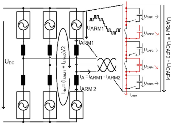
Figure 1.
Structure of the Modular Multilevel Converter.
2.2. Converter-Level Control
MMCs need controllers fulfilling several purposes: the control of external voltages and/or currents loops, the control of internal current loops and the control and balancing of the capacitor voltages [4].
2.2.1. Modulation Strategies of MMC
Several modulation techniques have been proposed in the literature [4,26,27,28,29,30]. In this paper, phase-shifted carrier pulse width modulation (PS-PWM) has been chosen, given the low number of submodules used in the prototype [26]. For a full-scale application with an increasing number of modules, other modulation schemes should be preferred, e.g., the Nearest Level Control [1].
2.2.2. Output Current and Energy Stored Control
The output current control in the MMC is similar to the control used in conventional 2-level VSC. For the internal control of MMC, two approaches can be used: Non-energy-based approach, where the output DC current is uncontrolled [17] and Energy-based control, where the energy stored in converter is controlled making use of the circulating currents [31], which are an intrinsic feature of the MMC converters. In this paper, an Energy-based control, already presented by the authors in [32], has been used to decouple the capacitor voltages from the DC bus. Figure 2a illustrates its working principle.
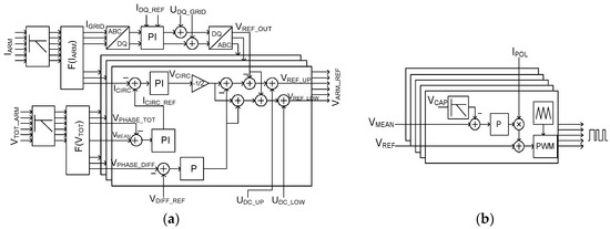
Figure 2.
(a) MMC control strategy diagram. IARM are the six arm currents of the MMC, IGRID are the three line currents of the utility grid computed using the block F(IARM) from the arm’s currents. ICIRC are the three-circulating currents in each phase of the MMC computed by the block F(IARM). ICIRC_REF is the circulating current reference in each phase. IDQ_REF are the AC line current references in the dq frame. UDQ_GRID are the three AC grid voltages in the dq frame. VREF_OUT are the three AC grid voltage references given by PI controllers. VTOT_ARM are the six total arms’ voltages. VPHASE_TOT is the total voltage of each phase of the MMC. VPHASE_DIF is the voltage difference between the upper and lower arms of the same phase. VDIF_REF is the voltage difference reference between the upper and lower arms of the same phase. UDC_LOW and UDC_UP are the half of DC grid voltage. VMEAN is the mean voltage of each phase. VARM_REF are the six arms’ voltage references given by the controller. P is a proportional controller; (b) Submodules capacitors voltage balancing strategy: VMEAN is the mean voltage of each arm. VCAP is the capacitor voltage of each submodule. VREF is the voltage reference of each submodule capacitor. IPOL gives the sign of the arm current. PWM is the block generating gates signals.
2.2.3. Capacitor Voltage Balancing
The sub-module voltage balancing is implemented to prevent the divergence of capacitor voltages, which would eventually result in the collapse of the entire system. Much research has dealt with SM voltage balancing techniques [26,27]. The strategy retained in this paper is based on what was presented in [32]. Figure 2b summarizes this balancing strategy; the meaning of all the involved signals is explained in the caption of Figure 2. In principle, each sub-module capacitor voltage is measured and compared with the mean value of all arm capacitor voltage. The difference resulting from this comparison, with a sign given by the arm current direction, is used by a proportional controller to provide a correction value which is added to the set point voltage given to the sub-module PWM generation.
2.3. MTDC Control Strategies
The control of a MTDC system focused on DC line voltage control and the control of the power exchange among HVDC stations. Several control strategies have been proposed in the literature. These include voltage margin control, voltage droop control, dead-band voltage droop control and non-dead band voltage control [33].
The voltage margin control method is an extension of the point-to-point HVDC transmission systems control. One of the terminals (also called master terminal or “slack-bus”) controls the DC voltage and the other terminals (slaves terminals) can arbitrarily (or based on available resources) inject or draw power. Controlling the MTDC network voltage at a single terminal has the drawbacks that the master converter is the only one to participate in the regulation of the DC voltage. It is, therefore, necessary that the AC network associated with the master converter can absorb or provide all the power variations necessary for the balance of the MTDC system, in particular in case of a fault. Moreover, the single terminal used as balanced terminal must be sized to cope with all power variations situations. This result is a weakness of the entire system since if the master converter is lost, the MTDC system will be no longer regulated and collapses [8].
In the voltage droop control method, the DC voltage variation is used as a common signal by all converters that adjust their power based on this DC voltage. Thus, the task of controlling the DC voltage is shared among all the converters. To stabilize the MTDC system, a dead zone can be added to the droop control setting, also called dead-band voltage droop control. This allows discrimination between normal and disturbed operation of the MTDC system. However, the control activity of the converters within the band (normal operation) is fully lost. This has the disadvantage that some of the droop control parameters are set to zero and infinity, which does not give any degree of freedom for optimization [34]. In the non-dead band voltage droop control, the dead zone is replaced by a real power-voltage characteristic slightly inclined. Therefore, different droop constants can be used, depending on the deviation between DC voltage set-point and measure. Several control characteristics of a non-dead band voltage control scheme are shown in Figure 3: a reference voltage and power are set for each converter, and the balancing of the system occurs by increasing the DC voltage in case of excess of power, while decreasing it otherwise. The slopes of the different sections of the characteristic are chosen according to the connected loads or sources (e.g., wind generators cannot usually provide large amounts of additional power). This method is effective to ensure stable operation of the DC network, also in case of a failure of one or even several converters.
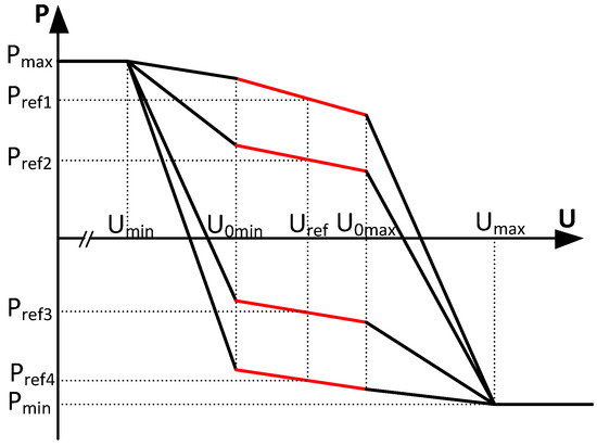
Figure 3.
Power-voltage control characteristics of a non-dead band voltage control [33].
3. MMC Control System Design
3.1. Overall Controller Operation
The MMC controller architecture is presented in Figure 4. A distributed controller architecture has been chosen, given the computational limitations of a centralized controller [35]. Compared to the distributed architecture presented in [35], a dedicated synchronization signal has been used here for an effective synchronization of all arm controllers. More details about the synchronization method are given in Section 3.3.4.
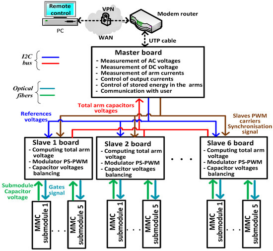
Figure 4.
Signals flows between controllers and power submodules.
All control and communication tasks are distributed between the “master” controller and the arms “slave” controllers. The master controller manages the real and reactive power flow, and the communications tasks with the external world. The master controller communicates to the six slave controllers the voltage references, the arm current signs, the synchronization signal of the arm controllers and other commands such as start driving submodules. Each slave controller periodically sends back to the master the total arm voltage and performs the balancing of its arm capacitor voltages using the arm current sign received from master.
3.2. Slave Controllers and Power Modules
The main tasks of the slave controllers consist of receiving each capacitor voltage, performing capacitor voltage balancing and generating command signals for each submodule. The slave controllers communicate with the master board using inter-integrated circuit bus (I2C), and with submodules using optical fibers. This ensure the insulation requirements between the control board and the power boards. The advantages of I2C bus are the reduced number of wires and the quite simple implementation in a multi-slave environment. The I2C fast mode has been chosen with a clock frequency of 350 kHz. Each arm controller is implemented using a TMS320F28335 TI C2000 DSP family. The frequency sent by the power submodule for the capacitor voltage measurement is measured by the enhanced capture (eCAP) peripheral of the DSP and then converted into voltage. The power submodules are driven by the slave controller through optical fibers. To prevent faults and generate the dead-times, the signals are pretreated by a programmable logic device (CPLD) before being sent to the gates. The capacitor voltages are measured using a voltage-controlled oscillator (VCO) which converts the capacitor voltage into a variable frequency signal. It is then sent to the corresponding arm controller through an optical fiber link. In this application, for a capacitor voltage range between 1 and 250 V, the VCO frequency varies linearly from 3 to 450 kHz. Each module has DC bus connectors and AC output connectors (middle points of H-bridge arms). Two PWM input signals are available to control the two IGBT legs. A 3.2 mF capacitor is connected between the DC bus for local power storage. In this paper, two IGBTs only (half-bridge operation) are mounted in the power module, requiring just one PWM input. The nominal ratings of the module are 10 A and 200 V, with some 1 kV isolation voltage. The low power supply for the sub-module is provided by a medium-frequency current-fed system, consisting of an isolated power supply and a cable passing through thirty small torus from the secondary of each torus, one for each sub-module [36]. An inverter fed a nominal current of 5 A in the cable at 45 kHz. Figure 5 presents the sub-module schematic and its hardware implementation. Table 1 give some specifications of the main power submodules devices.
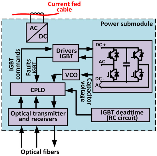
Figure 5.
Power submodule schematic (principle).

Table 1.
Main power submodule devices.
3.3. Master Controller
The master controller board is designed using a TI DSP Concerto F28M35x. The main tasks of the master board are the communication with the user or host, the digital conversion of measurements, the energy flow control, the start and stop tasks and the communication with the slave boards.
3.3.1. User Communication
The master communicates with operator through a User Interface (UI). It interacts with the M3 core of the master board using Ethernet protocol allowing, for instance, the converter to be compliant with IEC61850. Information such as real power, reactive power, nominal current, start and stop command are send to the master by the user through the UI. This feature allows command of the converter remotely in a Wide Area Network (WAN).
3.3.2. Start and Stop Tasks
Once the master controller receives start command from UI, switches connect the converter to the grid through pre-charge resistors. Flowcharts of the pre-charge and the shutdown of the MMC are presented in Figure 6.
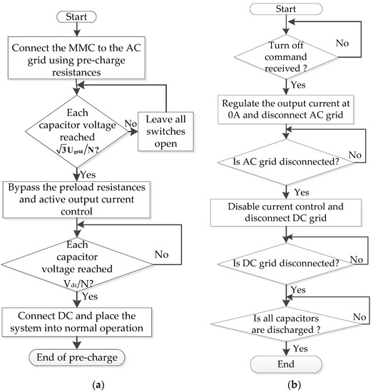
Figure 6.
Flowchart of the pre-charge and turn off strategy. (a) Pre-charge; (b) Turn off.
3.3.3. Current and Voltage Measurements and Energy Flow Control
ADC operations are performed by the C2000 core. Afterwards, PLL-based grid synchronization, AC current PI controllers and energy balancing are executed. The master controller is then able to send the six voltage references to each individual arm controller. To increase the bandwidth of the communication between master and slaves, the switching frequency has been chosen as one half of the sampling frequency. The arm voltage references are then updated every half period of the switching frequency; see details next section.
3.3.4. Communication and Synchronization with Slave Boards
Figure 7a shows the master controller data transfer process to the slaves in six sampling periods. Figure 7b,c show the communication protocol developed to meet the data transfer needs. The voltage references are coded with 12 bits.
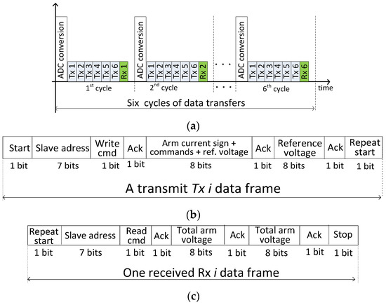
Figure 7.
Master to slaves communication protocols. (a) Master controller data transfer with slaves per ADC cycle of conversion. Tx i = transmit to slave i; Rx i = receipt from slave i; (b) data protocol used when sending messages to each slave; (c) data protocol used to receive message from each slave.
The four remaining bits are used to send the corresponding arm current sign and other commands to each slave such as the commands to start and stop the driving of submodules. All sending and receiving operations are performed within one sampling period. This protocol ensures that the voltage references and arm current sign, which are key information for the control, are updated and sent to slaves every sampling cycle. After three switching periods, the master has received the six arm voltages. This reception delay, caused by the low speed of I2C, is not so critical for the control since the capacitor voltage balancing is performed by the arm controllers. This delay has been taken into account in the controller design.
A distributed architecture of the controller requires an effective synchronization of all arm controllers, to ensure that the gates signals of all submodules are synchronized. To manage this issue, a dedicated synchronization signal is used as event trigger to adjust the phase of the first PWM on each of the six slave controllers. The other carriers of the same slave controller are referenced to the first carrier.
3.4. Protection Functions
Protection functions are included at various levels of the control system. The master controller redundantly checks for possible failures by analyzing the measurements received from ADC module. If a failure is detected, it sends the appropriate command to slave controllers to stop the submodules. The master also checks if a slave controller fails to communicate. In that case, it will also send the suitable command to the other slave boards to stop the whole converter. Submodule protections concerning power section faults, overvoltage and undervoltage are directly performed by the slave controllers. Their thresholds values are included in the capacitor’s voltage balancing scheme. If a non-critical failure occurs on a submodule, slave controller sends the appropriate command to bypass the faulty submodule. If the occurred failure is critical for the safe operation of the converter, the slave controller sends the appropriate command to the master and stops the entire arm. The last protection layer is performed by the CPLD on the submodule board. The CPLD uses a logic to protect the semiconductors in case of improper commands or incompatible capacitor voltage.
4. Experimental Validation
The proposed architecture has been implemented on a 5 kW reduced-scale MMC demonstrator. Figure 8 shows the whole MMC demonstrator. The main system parameters are shown in Table 2. Tests have been carried out with MMC working as inverter on a three-phase passive load with a DC link of 800 V and in a reduced-scale laboratory setup of a MTDC transmission network [25,37].

Figure 8.
Whole converter reduced-scale prototype.
Table 2.
Experimental setup.
The experimental validation of the control architecture and the overall functionality of the MMC includes several aspects. The communication between the master board and an UI, the data flow between the master and slave boards together with the synchronization of the generated PWM signals, and the operation of the modules driven by the slave boards have been tested.
The current and voltage waveforms as seen from the AC side, the MMC output current and energy stored control and the power flow control in a MTDC network have been tested too.
4.1. Communications Tests
To check the communication between master board and the UI, a hypertext transfer protocol (HTTP) has been used, allowing the master board to host a web page.
The correct flow of data between master board and slave boards has been tested, checking the information timing on the serial data line (SDA) and serial clock line (SCL) of the I2C bus. Figure 9 shows communication signals in compliance with the protocol presented in Figure 7a. The communication between master and slaves is effectively performed at each sampling period (half of the switching period). Data transfer duration between boards at each sampling cycle is about 400 µs, i.e., 80% of the period. The synchronization of PWM signals between two slave boards is also highlighted in Figure 9.
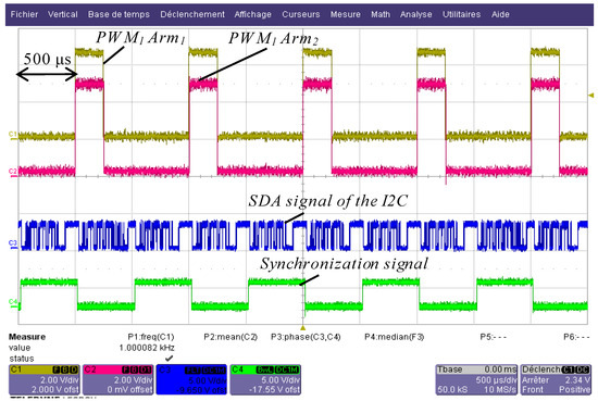
Figure 9.
Signals on the converter: PWM 1 signals of two arms controllers (duty cycle 25%), Serial data (SDA) line of the I2C (blue trace) and arms’ synchronization signal (green trace).
4.2. MMC Control Tests
4.2.1. Pre-Charge Test
The pre-charge is performed directly from the AC side without using any external power supply, in accordance with the flowchart presented in Figure 6a and to the fact that the module’s control is supplied independently of the capacitor voltage. The transient behavior of the voltage of a single SM capacitor during the pre-charge is presented in Figure 10.
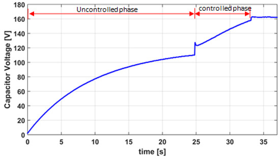
Figure 10.
Evolution over time of a submodule capacitor voltage during pre-charge.
During the uncontrolled phase, this evolution corresponds to the exponential charge waveform of a capacitor as expected. Bypassing the pre-charging resistors creates a voltage jump of approximately 15 V, due to the direct connection of the MMC to the AC network. The evolution of the voltage of each capacitor during the second phase is approximately linear, thanks to the output current controller that limits the current withdrawn from the AC side. With the chosen parameters, the entire pre-charge takes less than one minute.
4.2.2. Capacitor Voltage Balancing Test
During this test, the capacitor voltage balancing algorithm has simply been disabled and enabled for short periods the evaluation of its impact on the operation of the MMC. This test has been performed with the DC bus at 150 V to prevent any accidental capacitors failures. To better illustrate the dynamics of the balancing strategy at nominal voltage, some simulations were performed where all capacitor voltages were unbalanced with a large spread. Their initial values are: VC1 = 240 V, VC2 = 80 V, VC3 = 192 V, VC4 = 128 V and VC5 = 272 V.
Figure 11 presents the evolution over time of the capacitor voltages on the same arm in the two situations. It can be observed in Figure 11a that, when the algorithm is disabled, the SM capacitor voltages will not converge to their average value. Figure 11b shows that, when the balancing algorithm is activated, after about 0.2 s, all SM capacitor voltages converge to their average value. This result confirms the effectiveness of the SM capacitor balancing algorithm presented in Section 2.2.3.
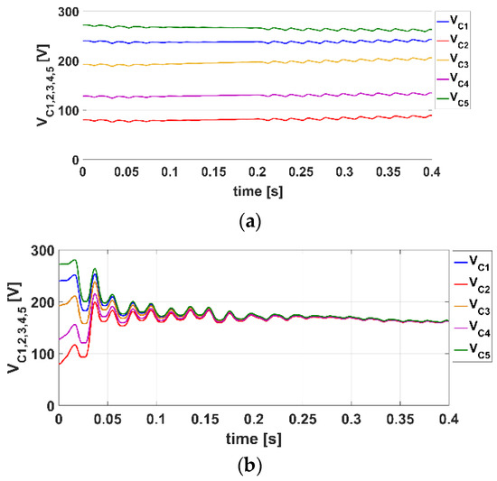
Figure 11.
Capacitor balancing test on the MMC, (a) With the balancing algorithm disabled; (b) With the balancing algorithm enabled.
4.2.3. Output Current and Energy Stored Control Tests
The output current controller has been tested with the MMC working as an inverter, supplied by a DC voltage of 800 V and injecting power into the AC utility grid. Figure 12 presents the dynamics of the controller during a change of the reference of the output current from 1 A to 3 A. The new reference value is reached in less than half a period of the output current denoting thereby a good dynamic of the regulator. The control of the energy stored in the converter is performed as presented in Section 2.2.2. Figure 13 presents the control of total arm voltages. In Figure 13a, the total arm voltages are not controlled. When the DC voltage changes, the total voltages of the upper and lower arms follow the DC voltage.
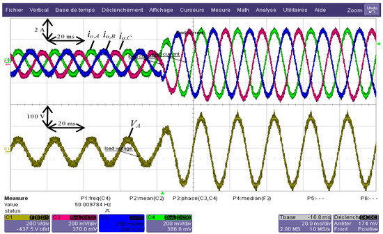
Figure 12.
Output current control: output currents and output voltage of the phase A.
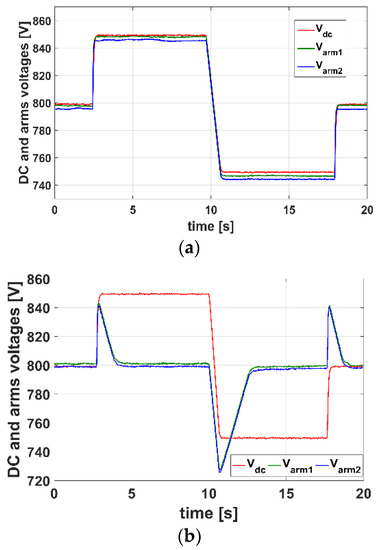
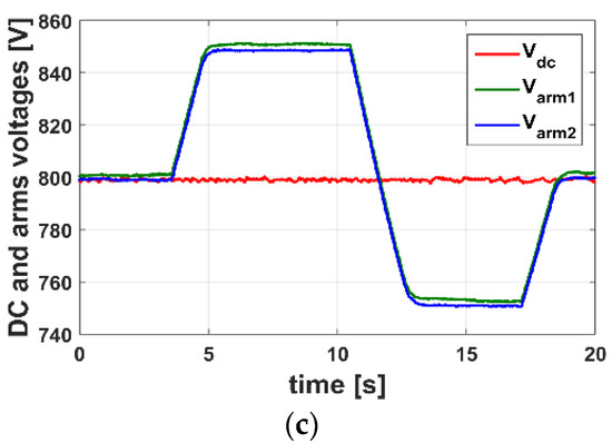
Figure 13.
Energy control tests results, (a) DC voltage, upper and lower arms total voltages without an energy control; (b) DC voltage, upper and lower arms total voltages with an energy control and step change in the DC voltage; (c) DC voltage, upper and lower arms total voltages with an energy control and step change of total arm voltages.
Hence the DC voltage is not decoupled from capacitor voltages. If a short time brake occurs in the DC bus, this will directly affect the capacitor voltages. In Figure 13b,c, the energy control is enabled. In Figure 13b, the total arm voltages are controlled at 800 V and the DC voltage steps successively from 800 V to 850 V, from 850 V to 750 V and from 750 V to 800 V. After a short transient phase, the total arm voltages remain at their reference value. In Figure 13c, the DC voltage is held at 800 V and the total arm voltages are set to step successively from 800 V to 850 V, from 850 V to 750 V and from 750 V to 800 V. The energy control allows a decoupling between capacitor voltages and the DC bus voltage. The dynamics of the total arm voltage control loop has been intentionally reduced to avoid overvoltage on the capacitors.
4.3. Power Flow Control in a MTDC Network
The MMC has been implemented in a reduced-scale laboratory setup to test system-level control algorithms. Figure 14 shows the MTDC mock-up previously developed and described in [1]. The laboratory set-up presented in Figure 14b simulates the following imaginary situation: Three converters, namely VSCDELTA, VSCGAMMA, and the MMC, simulate an MTDC connection between three different AC grids. This could be the case as an example of the connection between Italy, Sardinia, and Corsica, actually made with thyristors technology. All converters are implemented with independent controllers to test the stability of the DC grid. A non-dead band voltage control [37] has been implemented on VSCDELTA and VSCGAMMA converters while the MMC controls the power injected in the AC grid. Several tests have been performed to verify the functionalities of the MMC when connected to a MTDC transmission network. The DC lines have been (roughly) simulated with a lumped parameters π equivalent circuit.
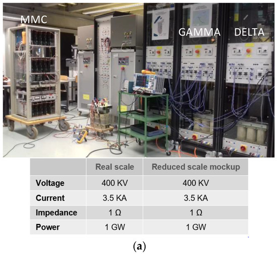
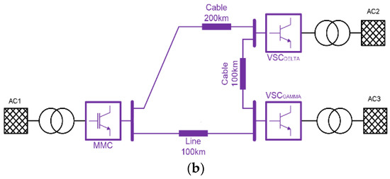
Figure 14.
MTDC mockup, (a) MTDC mockup on laboratory; (b) Single line diagram of the laboratory setup.
In a first test, different power profiles have been imposed on the AC side and corresponding powers are absorbed by the MMC on the DC side, as illustrated in Figure 15a. On the DC side, the stability of the DC network is secured, showing the effectiveness of the non-dead band voltage control. On the MMC side, the energy control allows maintaining of a stable voltage in the converter’s sub-modules, decoupling them from the DC-link voltage variations as illustrated in Figure 15b.
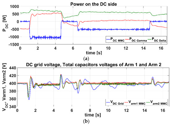
Figure 15.
MTDC results with a variation of power transmitted in the onshore AC grid, (a) Power variations in the experimental set-up with controlled MMC and two inverters implemented with non-dead band voltage control; (b) DC voltage variation and two arms of the MMC voltages during power flow.
A second test was performed to observe the whole MTDC system behavior when the SM of the MMC are used to store and restore energy in the system. The power transmitted between the DC and the AC1 grid remains constant. The DC voltage variation and two arms of the MMC voltages are shown in Figure 16a, and the power variations on the three VSC are shown in Figure 16b. It can be seen in Figure 16 that the DC bus is not affected by these energy variations on the MMC and that the transients due to these charges and discharges are well absorbed.
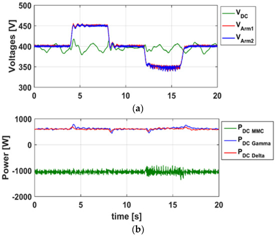
Figure 16.
MTDC results when the stored energy in the MMC varies, (a) DC voltage variation and two arms of the MMC voltages; (b) Power variations in the experimental set-up with controlled MMC and two inverters implemented with non-dead band voltage control.
A third test was run to test the MTDC system with all VSC implementing the non-dead band droop control. Figure 17 presents the DC link voltage and power variation over the three converters when slight power variations are provoked. It can be seen on Figure 17 that the DC bus is well controlled, and the transients are well absorbed by the three converters when the entire system is facing power variations. This third scenario also highlights the contribution of each converter to the stability of the DC bus.
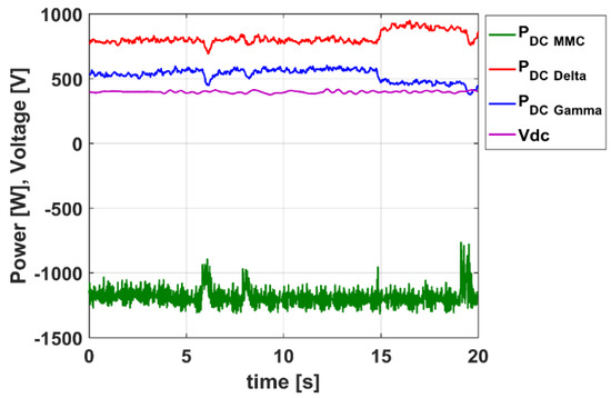
Figure 17.
MTDC results when all VSC implement Non-dead band droop control.
Those results confirm the correct behavior of the MMC in a MTDC system and against power variation.
5. Discussion and Further Improvements
Concerning the controller architecture presented in this paper, the goal was to propose a light architecture with well-known DSP that could be quickly built and that could successfully be implemented in a small-scale prototype to test the control strategies developed. One critical point of this control structure is its scalability in case of a higher number of modules. Due to its decentralized architecture, in principle it is suitable for a higher number of SM in each arm, because all the operations assigned to the master controller and the communication between the master and the slave controllers do not depend on the number of SM to control. The local management of each arm is performed by an independent controller sending the reference set-points to all PWM modulators. However, the DSP used has twelve independent PWM outputs, so a maximum number of 12 modules can be controlled, without acting on the slave hardware.
For more modules, the slave controller could be combined, or even replaced by a low-cost FPGA that would produce as many PWM outputs as required. In case of combination of the slave DSP and an FPGA, the capacitor balancing and sorting algorithms which are sequential operations remain the task of the DSP. These aspects are under development and will not be discussed further in this paper.
The proposed hardware structure will be used for a lower demanding application in terms of voltage rating, i.e., a medium-voltage application such as a MV-Statcom or MV-SOP (Soft Open Point). In this case, the number of modules to be managed is about 20–24, which is feasible with the proposed multi-DSP approach.
Another critical point is the robustness of the I2C bus. It appeared a few times during tests in a highly EM perturbed environment that the I2C bus was perturbed when the bus was not shielded enough. However, all the EMC problems in the prototype have been solved with suitable shielding and accurate state-machine and communication tuning to avoid critical situations, such as the switching of the main contactors.
6. Conclusions
This paper presents the design and the implementation of a small-scale modular multilevel converter. The proposed MMC prototype has been used to test both converter and system-level controls in a reduced-scale MMC-based MTDC network. Several MMC control levels have been tested and the results obtained validated the control strategies implemented and the controller architecture designed. The tests performed at system level have enabled exploration of the advantages of using an MMC-based MTDC system, which include the capability of the MMC to store and restore the energy in the system, its scalability which allows the extension of the DC link voltage as desired, and improvement to the AC side voltage harmonics contents.
Author Contributions
Conceptualization, E.T.L., S.G., D.S. and M.C.; Formal analysis, all authors; Funding acquisition, M.C.; Software, E.T.L., S.G. and D.S.; Supervision, M.C.; Validation, all authors; Writing—original draft, E.T.L.; Writing—review & editing, E.T.L. and M.C.
Funding
The authors acknowledge EOS-Holding (CH) for the funding of the research presented in this paper. This research is part of the activities of the Swiss Centre for Competence in Energy Research on the Future Swiss Electrical Infrastructure (SCCER-FURIES), which is financially supported by the Swiss Innovation Agency (Innosuisse-SCCER program).
Acknowledgments
The authors would like to thank P. Favre-Perrod, D. Leu, H. Parisod (HES-SO), J. Braun (CERN) for their contributions and useful suggestions.
Conflicts of Interest
The authors declare no conflict of interest.
References
- Siemaszko, D.; Carpita, M.; Favre-Perrod, P. Conception of a modular multilevel converter in a multi-terminal DC/AC transmission network. In Proceedings of the Power Electronics and Applications (EPE’15 ECCE-Europe), Geneva, Switzerland, 8–10 September 2015. [Google Scholar] [CrossRef]
- Lesnicar, A.; Marquardt, R. An innovative modular multilevel converter topology suitable for a wide power range. In Proceedings of the IEEE Bologna Power Tech Conference, Bologna, Italy, 23–26 June 2003. [Google Scholar] [CrossRef]
- Sharifabadi, K.; Harnefors, L.; Nee, H.P.; Norrga, S.; Teodorescu, R. Design, Control, and Application of Modular Multilevel Converters for HVDC Transmission Systems; Wiley-IEEE Press: Hoboken, NJ, USA, 2016. [Google Scholar]
- Perez, M.A.; Bernet, S.; Rodriguez, J.; Kouro, S.; Lizana, R. Circuit topologies, modelling, control schemes and applications of modular multilevel converters. IEEE Trans. Power Electron. 2015, 30, 4–17. [Google Scholar] [CrossRef]
- Dorn, J.; Gambach, H.; Strauss, J.; Westerweller, T.; Alligan, J. Transbay cable-A breakthrough of VSC multilevel converters in HVDC transmission. In Proceedings of the CIGRE San Francisco Colloquium, San Francisco, CA, USA, 7–9 March 2012. [Google Scholar]
- Francos, P.L.; Verdugo, S.; Alvarez, H.F.; Guyomarch, S.; Loncle, J. INELFE—Europe’s first integrated onshore HVDC interconnection. In Proceedings of the IEEE Power and Energy Society General Meeting, San Diego, CA, USA, 22–26 July 2012. [Google Scholar]
- Hussennether, V.; Rittiger, J.; Barth, A.; Worthington, D.; Rapetti, D.G.M.; Huhnerbein, B.; Siebert, M. Project borwin2 and helwin1-large scale multilevel voltage sources converter technology for bundling of offshore windpower. In Proceedings of the CIGRE, Paris, France, 26–31 August 2012. [Google Scholar]
- Zhang, L.; Zou, Y.; Yu, J.; Qin, J.; Vittal, V.; Karady, G.; Shi, D.; Wang, Z. Modeling, control, and protection of modular multilevel converter-based multi-terminal HVDC systems: A review. CSEE J. Power Energy Syst. 2017, 3, 340–352. [Google Scholar] [CrossRef]
- Ronanki, D.; Williamson, S. Modular Multilevel Converters for transportation electrification: Challenges and opportunities. IEEE Trans. Transport. Electrification 2018, 4, 399–407. [Google Scholar] [CrossRef]
- Van Hertem, D.; Ghandhari, M. Multi-terminal VSC HVDC for the European supergrid: Obstacles. Renew. Sustain. Energy Rev. 2010, 14, 3156–3163. [Google Scholar] [CrossRef]
- Bucher, M.K.; Franck, C.M. Fault current interruption in multiterminal HVDC networks. IEEE Trans. Power Deliv. 2015, 31, 87–95. [Google Scholar] [CrossRef]
- Li, R.; Xu, L.; Yao, L.; Williams, B.W. Active control of DC fault currents in DC solid-state transformers during ride-through operation of multi-terminal HVDC systems. IEEE Trans. Energy Convers. 2016, 31, 1336–1346. [Google Scholar] [CrossRef]
- Egea-Alvarez, A.; Bianchi, F.; Junyent-Ferre, A.; Gross, G.; Gomis-Bellmunt, O. Voltage control of multiterminal VSC-HVDC transmission systems for offshore wind power plants: Design and implementation in a scaled platform. IEEE Trans. Ind. Electron. 2013, 60, 2381–2391. [Google Scholar] [CrossRef]
- Aragüés-Peñalba, M.; Egea-Àlvarez, A.; Galceran Arellano, S.; Gomis-Bellmunt, O. Droop control for loss minimization in HVDC multi-terminal transmission systems for large offshore wind farms. Electr. Power Syst. Res. 2014, 112, 48–55. [Google Scholar] [CrossRef]
- Debnath, S.; Qin, J.; Bahrani, B.; Saeedifard, M.; Barbosa, P. Operation, control, and applications of the modular multilevel converter: A review. IEEE Trans. Power Electron. 2015, 30, 37–53. [Google Scholar] [CrossRef]
- Belhaouane, M.; Freytes, J.; Ayari, M.; Colas, F.; Gruson, F.; Braiek, N.; Guillaud, X. Optimal control design for Modular Multilevel Converters operating on multi-terminal DC Grid. In Proceedings of the 2016 Power Systems Computation Conference (PSCC), Genova, Italy, 20–24 June 2016; pp. 1–7. [Google Scholar] [CrossRef]
- Ji, H.; Chen, A.; Liu, Q.; Zhang, C. A new circulating current suppressing control strategy for modular multilevel converters. In Proceedings of the 36th Chinese Control Conference (CCC), Dalian, China, 26–28 July 2017; pp. 9151–9156. [Google Scholar] [CrossRef]
- Zama, A.; Benchaib, A.; Bacha, S.; Frey, D.; Silvant, S. High dynamics control for MMC based on exact discrete-time model with experimental validation. IEEE Trans. Power Deliv. 2018, 33, 477–488. [Google Scholar] [CrossRef]
- Zhou, Y.; Jiang, D.; Hu, P.; Guo, J.; Liang, Y.; Lin, Z. A prototype of modular multilevel converters. IEEE Trans. Power Electron. 2014, 29, 3267–3278. [Google Scholar] [CrossRef]
- Binbin, L.; Dandan, X.; Dianguo, X.; Rongfeng, Y. Prototype design and experimental verification of modular multilevel converter based back-to-back system. In Proceedings of the International Symposium on Industrial Electronics, Istanbul, Turkey, 1–4 June 2014; pp. 626–630. [Google Scholar]
- Moranchel, M.; Sanchez, F.M.; Bueno, E.J.; Rodriguez, F.J.; Sanz, I. Six-level modular multilevel converter prototype with centralized hardware platform controller. In Proceedings of the IECON 2015, Yokohama, Japan, 9–12 November 2015; pp. 863–868. [Google Scholar]
- Jasim, O.F.; Moreno, F.J.; Trainer, D.R.; Feldman, R.; Farr, E.M.; Claree, J.C. Hybrid experimental setup for alternate arm converter and modular multilevel converter. In Proceedings of the 13th IET international conference on AC and DC Power Transmission, Manchester, UK, 14–16 February 2017; pp. 1–6. [Google Scholar]
- Islam, M.R.; Guo, Y.; Zhu, J. FPGA-based control of modular multilevel converters: Modeling and experimental evaluation. In Proceedings of the International Conference on Electrical & Electronic Engineering (ICEEE), Rajshahi, Bangladesh, 4–6 November 2015; pp. 89–92. [Google Scholar]
- Lago, J.; Sousa, G.J.M.; Heldwein, M.L. Digital control/modulation platform for a modular multilevel converter system. In Proceedings of the COBEP, Gramado, Brazil, 27–31 October 2013; pp. 271–277. [Google Scholar]
- Luginbühl, M.; Pidancier, T.; Favre-Perrod, P. Transmission d’énergie par réseaux à courant continu multiterminaux. Bull. AES/Electrosuisse 2014, 12, 70–74. [Google Scholar]
- Hagiwara, M.; Akagi, H. Control and experiment of pulse width modulated modular multilevel converters. IEEE Trans. Power Electron. 2009, 24, 1737–1746. [Google Scholar] [CrossRef]
- Siemaszko, D. Fast sorting method for balancing capacitor voltages in modular multilevel converters. IEEE Trans. Power Electron. 2015, 30, 463–470. [Google Scholar] [CrossRef]
- Ängquist, L.; Antonopoulos, A.; Siemaszko, D.; Ilves, K.; Vasiladiotis, M.; Nee, H.P. Open-loop control of modular multilevel converters using estimation of stored energy. IEEE Trans. Ind. Appl. 2011, 47, 2516–2524. [Google Scholar] [CrossRef]
- Edpuganti, A.; Rathore, A.K. Optimal pulsewidth modulation of medium-voltage modular multilevel converter. IEEE Trans. Ind. Appl. 2016, 52, 3435–3442. [Google Scholar] [CrossRef]
- Franquelo, L.G.; Rodriguez, J.; Leon, J.I.; Kouro, S.; Portillo, R.; Prats, M.M. The age of multilevel converters arrives. IEEE Trans. Ind. Electron. Mag. 2008, 2, 28–39. [Google Scholar] [CrossRef]
- Delarue, P.; Gruson, F.; Guillaud, X. Energetic macroscopic representation and inversion based control of a modular multilevel converter. In Proceedings of the 15th European Conference on Power Electronics and Applications (EPE’13 ECCE Europe), Lille, France, 3–5 September 2013; pp. 1–10. [Google Scholar]
- Siemaszko, D.; Talon Louokdom, E.; Parisod, H.; Braun, J.; Gavin, S.; Eggenschwiler, L.; Favre-Perrod, P.; Carpita, M. Implementation and experimental set-up of a Modular Multilevel Converter in a Multi Terminal DC/AC transmission network. In Proceedings of the 18th European Conference on Power Electronics and Applications (EPE’16 ECCE Europe), Karlsruhe, Germany, 5–9 September 2016; pp. 1–12. [Google Scholar]
- Luginbühl, M.; Lalou, M.J. Contrôle coordonné des convertisseurs de réseaux MTDC. Bull. AES/Electrosuisse 2013, 12, 36–39. [Google Scholar]
- Vrana, T.K.; Zeni, L.; Fosso, O.B. Active power control with undead-band voltage & frequency droop for HVDC converters in large meshed DC grids. In Proceedings of the EWEA Conference, Copenhagen, Denmark, 16–19 April 2012. [Google Scholar]
- Talon, E.L.; Gavin, S.; Siemaszko, D.; Biya-Motto, F.; Essimbi, B.Z.; Carpita, M. Design and implementation of a multi-dsp based digital control system architecture for modular multilevel converters. In Proceedings of the IEEE-PEMC, Varna, Bulgaria, 25–30 September 2016; pp. 1182–1187. [Google Scholar]
- Wen, H.; Xiao, W.; Lu, Z. Current-fed high-frequency AC distributed power system for medium–high-voltage gate driving applications. IEEE Trans. Ind. Electron. 2013, 60, 3736–3751. [Google Scholar] [CrossRef]
- Talon Louokdom, E.; Siemaszko, D.; Gavin, S.; Leu, D.; Favre-Perrod, P.; Carpita, M. Use of Modular Multilevel Converter in multi-terminal DC transmission network: Reduced scale set-up and experimental results. In Proceedings of the 19th European Conference on Power Electronics and Applications (EPE’17 ECCE Europe), Warsaw, Poland, 11–14 September 2017; pp. P.1–P.9. [Google Scholar]
© 2018 by the authors. Licensee MDPI, Basel, Switzerland. This article is an open access article distributed under the terms and conditions of the Creative Commons Attribution (CC BY) license (http://creativecommons.org/licenses/by/4.0/).