Article

Disturbance Rejection Control Method of Double-Switch Buck-Boost Converter Using Combined Control Strategy

1
College of Automation, Harbin Engineering University, Harbin 150001, China
2
School of Light Industry, Harbin University of Commerce, Harbin 150001, China
*
Author to whom correspondence should be addressed.
Energies 2019, 12(2), 278; https://doi.org/10.3390/en12020278
Submission received: 10 December 2018 / Revised: 4 January 2019 / Accepted: 7 January 2019 / Published: 16 January 2019
(This article belongs to the Special Issue Control in Power Electronics)

Abstract

:
Since it has strong ability to realize a conversion to adapt to a wide variation of input voltage, the double-switch buck-boost (DSBB) converter is usually employed as a front-end converter in two-stage power converter systems, where conversion efficiency is always highly valued. Because there is only one switch in the Pulse Width Modulation (PWM) state in the buck or boost work mode, the combined control scheme was investigated for its advantages in inductor average current and conversion efficiency. However, in this method, the operation mode should be determined by additional logic according to the change of input voltage. Moreover, different control systems should be designed for different operation modes to guarantee dynamic control performance and smooth transition between different work modes. To address these issues, the linear active disturbance rejection control (LADRC) method is introduced to develop an inner current control loop in this paper. In this method, the model deviations in different work modes are considered as a generalized disturbance, and a unified current control plant can be derived for current controller design. Furthermore, the duty cycle limitations in practice are considered, an additional mode for transitional operation is produced, and the corresponding control scheme is also developed. Simulation and experimental test results are provided to validate the correctness and effectiveness of the proposed control scheme.

1. Introduction

The double-switch buck-boost converter has the ability to convert an input voltage with a wide change range to a desired output voltage, therefore, it is usually employed as a front-end converter in two-stage power conversion systems [1], such as in single-phase power factor correction applications [2,3], fuel cell generation [4], solar applications [5], hybrid energy storage systems [6], electric vehicle applications [7], etc. As presented in Figure 1, the topology of this converter is constituted through series connection of a traditional buck and boost circuit. Though the double-switch buck-boost converter has only two switches, there are several modulation and control methods that have been studied for it from different perspectives to obtain different performances in inductor ripple current, conversion efficiency, control complexity, etc.
The synchronization modulation method introduced in Reference [8] is the simplest scheme used for double-switch buck-boost converter, the driving pulses of S1 and S2 are in phase and the duty cycles of the two driving pulses are the same in this method. Though the synchronization modulation method is very convenient in implementation, the inductor ripple current, average currents, and the inductor magnetic core loss are relatively high. A large inductor can be adopted to suppress the inductor ripple current in this condition, however, this might cause unexpected impact on power density and cost. The interleaved modulation method that is proposed in Reference [9] can result in a much lower inductor ripple current, in contrast to the synchronization method, the switching signals have the same duty cycles and there is 180° phase shifting between the driving signals of S1 and S2. Furthermore, due to the direct power transmission mode in this method, the conversion efficiency of double-switch buck-boost converter can be enhanced accordingly by using interleaved modulation scheme [10]. Although the inductor ripple current using this modulation method can be significantly reduced, and the conversion efficiency can be enhanced too, the inductor average current is still relatively high as same as that using the synchronization modulation method. This issue becomes more and more prominent when the input voltage is relatively low that will cause a larger inductor average current and power losses.
The combined control strategy proposed in References [11,12,13,14,15] has relatively higher conversion efficiency and lower inductor average current compared to the interleaved and synchronization modulation methods. In this method, there are two separated buck and boost work modes, while only one operating mode is active at a time depends on the relationship between the value of input voltage and output voltage. For example, the boost work mode is active when the output voltage is higher than the input voltage, and in this mode, S1 is in on state and S2 is controlled using PWM scheme to get desired output voltage. The buck mode will be triggered when the output voltage is lower than the input voltage, in this case, S1 is controlled using PWM scheme, while S2 is always in off state. This control method is beneficial to obtain relatively low inductor average current and high power conversion efficiency, however, additional control logic and compensation methods are required to guarantee smooth switching between buck and boost modes [16,17], which means that the control system has the ability to adapt the change of input and output voltage without an intense transient state process. Furthermore, since the small signal models for inductor current and output voltage control system design in buck and boost modes are completely different, an increase in the complexity of the controller design will occur. In References [18,19,20], the uncertainty and disturbance estimator (UDE)-based control methods are utilized for the bidirectional noninverting buck-boost converter with multimode operation. Particularly, as in Reference [19], the tradeoff between tracking and disturbance rejection is investigated under finite control bandwidth constraints, and design guidelines are presented to achieve optimal performance in disturbance rejection. In Reference [20], the guidelines for UDE-based controllers design under typical actuator constraints are revealed, since the desired phase margin will decrease the available control bandwidth, the tradeoff between tracking and disturbance rejection will then become more conservative accordingly. However, in the mentioned UDE-based control method, the differential operation of the state variable is inevitable in the estimation of model uncertainty and external disturbance, and since an open loop estimator (calculation based) is adopted in this method, the accuracy of estimation completely depends on the accuracy of sampling data. Therefore, these issues might increase the threshold in practical application with higher power requirement.
The LADRC method has capacity to tolerate model deviation and it possesses an inherent disturbance rejection ability which are useful for control system design [21]. The external interferences, parameter perturbations, and impacts of model deviations can all be processed as a generalized disturbance in this method [22]. The generalized disturbance, as well as the state variables, can be observed by employing the closed loop linear extended state observer technique (LESO) proposed in References [23,24]; the control signal can be synthesized by utilizing the estimated signals. In such a system, the negative impacts of external disturbance and model deviation can be effectively compensated if the generalized disturbance and state variables can be observed accurately by LESO [25,26].
In this study, a unified current control plant is derived for inner current loop design in different control modes, the LADRC method is employed to improve the dynamic control performance of a double-switch buck-boost (DSBB) converter, and realize a smooth transition between the two separated operating modes of DSBB converter. Compared to traditional combined control method, there is no need for developing a complex logic to determine the work mode and the corresponding controller of DSBB converter. This paper is organized in five sections. The principle of the proposed modulation scheme, performance analysis and the small signal model for the double-switch buck-boost converter are discussed in Section 2. The proposed control system scheme is presented in Section 3. The control system design, simulation, and experimental results are given in Section 4. Finally, the conclusions are drawn in Section 5.

2. Topology, Modulation Method and Modeling

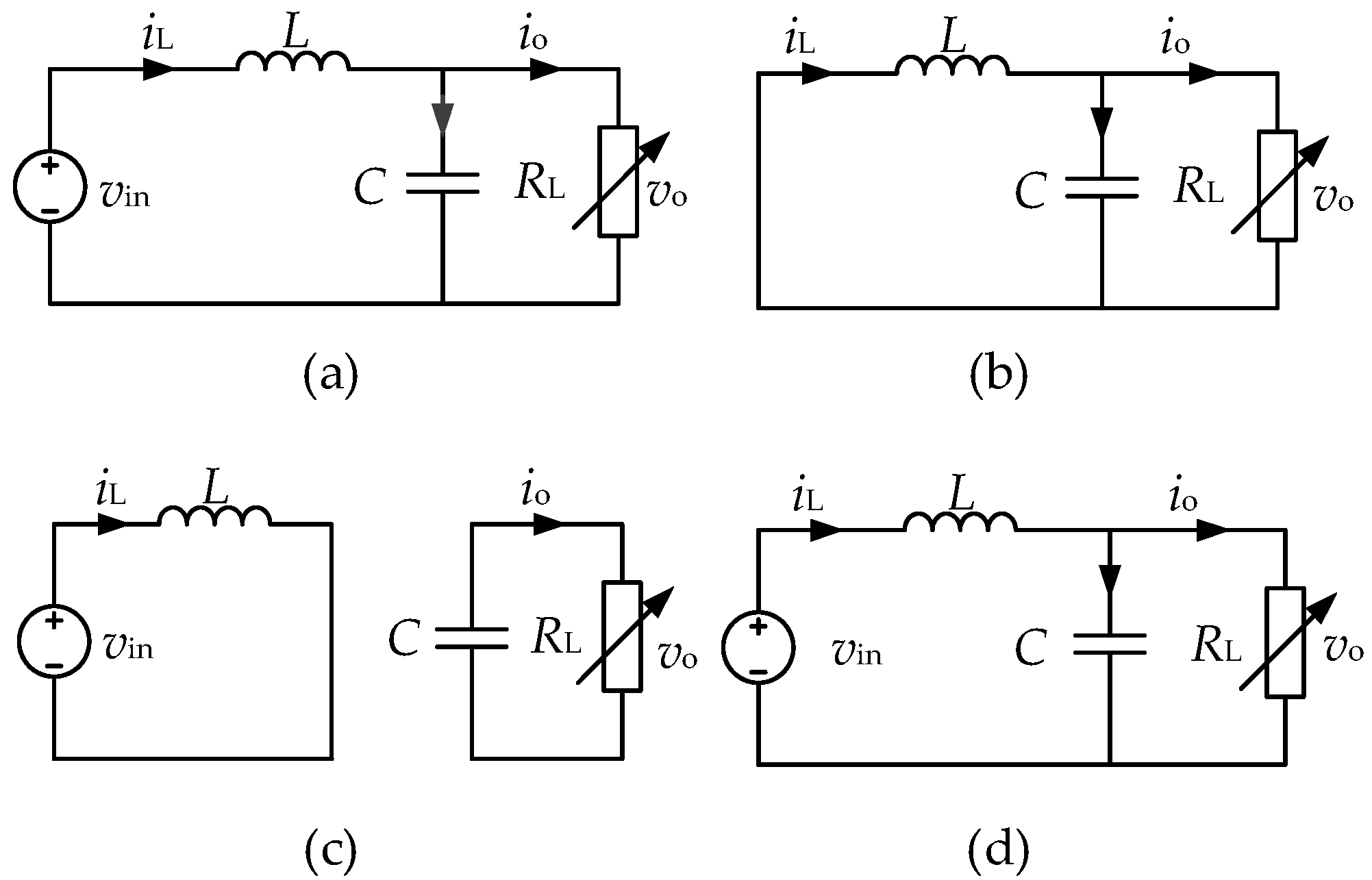
2.1. Principles of the Proposed Scheme

The topology of the DSBB converter is shown in Figure 1, in this figure, vin and vo are the input and output voltages, respectively. iL is inductor current, io is output current, and RL is load resistor. In combined modulation method, if vin > vo, S1 is active in PWM mode and S2 is in the OFF state, and the converter behaves like a buck converter; otherwise, S2 is active in PWM mode and S1 is always in the ON state, and the converter acts as a boost converter.
In Figure 1, the duty cycles, d1 and d2 of S1 and S2, respectively, are defined as (1).
{ d 1 = d + c d 2 = d c
In (1), d is a variable outputted by controller and c is a fixed offset value. It is assumed that d1 and d2 have the same upper and lower limits given by (2).
{ d min d 1 d max d min d 2 d max ,   ( d min   +   d max   =   1 )
In this paper, if the value of d1 or d2 is higher than dmax (e.g., 98%), then the corresponding switch will be always turned on, while if d1 or d2 is lower than dmin (e.g., 2%), then S1 or S2 will always be turned off. This practical duty cycle limitation is applied to avoid very narrow pulse, and guarantee reliable switching of S1 and S2.
For (2), if the values of d1 and d2 are out of their boundaries, the inequalities (3) and (4) will be artificially adopted in actual digital control system through very simple comparison. For example, if d 1   >   d max , then the value of d1 will be set to a number larger than the one in the control system meaning that S1 is always in the ON state.
{ d 1 1 ,   if   d 1 > d max d 2 1 ,   if   d 2 > d max
{ d 1 0 ,   if   d 1 < d min d 2 0 ,   if   d 2 < d min
Considering the aforementioned duty cycle limitation conditions in (2), there are three operation regions can be defined for the DSBB converter using combined control method. As shown in Figure 2, vinmin and vinmax are the minimum and the maximum values of the input voltage respectively, the upper boundary of the shadow area is v o / d max , and the lower boundary of the shadow area is v o d max .
In this figure, if v o / d max     v in     v inmax (as the zone denoted by A), the DSBB converter should work in buck mode, in this case, S1 is operated under PWM control, while S2 is always in the OFF state. Assuming the inductor, L is in continuous conduction mode, and (5) should be satisfied in this condition.
{ v o v inmax d + c d max d c 0 ,   ( d c < d min )
Combining the two inequalities in (5), a constraint condition for c can be obtained as (6).
c v o 2 v inmax
Similarly, if v inmin     v in     v o d max (as the zone denoted by B), the DSBB converter should work in boost mode, and supposing that the inductor is also in continuous conduction mode, (7) should be satisfied in this condition.
{ d min d c 1 v inmin v o d + c 1 ,   ( d + c > d max )
In this case, another limitation condition of c can be deduced as in (8).
c v inmin 2 v o
The shadow area ( v o d max   <   v in   <   v o / d max ) denoted by C is a transitional zone. In this zone, S1 and S2 are always kept in the ON and OFF states, respectively.
{ d + c 1 ,   ( d + c d max ) d c 0 ,   ( d c d min )
(10) can be derived from (9).
c 0.5
Therefore, (11) can be deduced by combining (6), (8), and (10).
1 > c max ( v o 2 v inmax ,   v inmin 2 v o ,   0.5 ) = 0.5
From (11), it can be concluded that the value of duty cycle offset, c can be selected regardless of the values of vin, dmax, and dmin in combined control method of DSBB converter. However, the width of the shadow area in Figure 2 is defined by the values of dmax and dmin, which means that the control accuracy is degraded when the value of input voltage is close to the output voltage. Therefore, the value of dmax is hoped as large as possible while the two switches, S1 and S2 can work well in practices.
In this paper, S1 and S2 are switched sharing the same carrier wave with combined control scheme, the double-switch buck-boost converter can be controlled to operate in any zone in Figure 2 automatically without any additional logic judgement to determine the work mode or the corresponding control method.

2.2. Small Signal Model

Control-oriented models are addressed in this section for output voltage and inductor current based dual-loop control system design. The converter should be operated in buck and boost modes, and the transfer functions in different work modes should be formulated for control system design. Since the buck and boost converter all have nonlinear properties, the small signal modeling method is adopted in this paper. The switching modes of double-switch buck-boost converter are shown in Figure 3. In Figure 3, (a) and (b) are in buck mode and (c) and (d) are in boost mode. Ts represents the switching period.
In buck mode, (12) can be obtained using Figure 3a,b.
{ L d i L d t = ( d + c ) v in v o C d v o d t = i L v o R L
In boost mode, (13) can be obtained using Figure 3c,d.
{ L d i L d t = v in ( 1 d + c ) v o C d v o d t = ( 1 d + c ) i L v o R L
By introducing small signal disturbance, i ˜ L , v ˜ o , v ˜ in , and d ˜ , of iL, vo, vin, and d, respectively, the small signal model of the converter operated in buck and boost mode can be expressed in (14) and (15), respectively. Vin and Vo are the steady state values of vin and vo respectively.
{ L d i ˜ L d t = d ˜ V in + ( D + c ) v ˜ in v ˜ o C d v ˜ o d t = i ˜ L v ˜ o R L ,   Buck   mode
{ L d i ˜ L d t = ( 1 D + c ) v ˜ o + v ˜ in + d ˜ V o C d v ˜ o d t = ( 1 D + c ) i ˜ L v ˜ o R L d ˜ I L ,   Boost   mode
By defining
K N = V in + V o 2
the first equation in (14) and (15) can be integrated as (17):
L d i ˜ L d t = K N d ˜ + f ˜
where,
f ˜ = { ( D + c ) v ˜ in v ˜ o + ( V in K N ) d ˜             ,   Buck   mode v ˜ in ( 1 D + c ) v ˜ o + ( V o K N ) d ˜ ,   Boost   mode
From control point of view, if f ˜ is taken as a disturbance and it can be properly compensated by inductor current control system, then the DSBB converter in buck and boost modes has the same inductor current control plant as shown in (19). s is the Laplace operator.
G ld = i ˜ L d ˜ | f ˜ = 0 = K N s L
From (14), the transfer function i ˜ L -to- v ˜ o in buck mode can be deduced as (20).
G 1 = v ˜ o i ˜ L = R L s C R L + 1
Similarly, the transfer function of i ˜ L -to- v ˜ o in boost mode can be formulated in (21) using (15).
G 2 = v ˜ o i ˜ L = R L ( 1 D + c ) L s 1 D + c s C R L + 2

3. Control Strategy for DSBB

3.1. LADRC Based Current Control Loop

As shown in (17), d ˜ is control signal for inner current loop and f ˜ can be considered as a generalized disturbance that is associated with both inner and outer variable factors of the inductor current control systems (e.g., the value of input/output voltage, operating point related steady state value of D, uncertain dynamic caused by work mode transition, etc.). In practical situations, f ˜ is usually unknown and cannot be directly measured. Therefore, LESO is adopted to evaluate it as well as the other relevant state variables in the LADRC method.
x   =   [ i ˜ L f ˜ ] T is selected as the state vector, the augmented state space model is formulated by (22)
{ x ˙ = A x + B d ˜ + E f ˜ ˙ i ˜ L = C x
where,
{ A = [ 0 1 0 0 ] B T = [ K N 0 ] E T = [ 0 1 ] C = [ 1 0 ]
The LESO is constructed by (24):
{ z ˙ = A z + B u + L ( y y ^ ) = A z + B u + L ( y C z ) y ^ = C z
In (24), z   =   [ z 1 z 2 ] T is estimated vector of x and L is the observer gain.
Since f ˜ ˙ is unknown and it can be estimated through the correction in (24), f ˜ ˙ is omitted in (24). By defining ω c   =   [ d ˜ i ˜ L ] T , (24) can be rewritten as (25).
{ z ˙ = [ A L C ] z + [ B L ] w c y c = z
In (25), the observer gain, L can be designed using the pole placement method proposed in [22].
L = [ 2 ω oc ω oc 2 ] T
where, ω oc is the equivalent bandwidth of the observer.
Assuming f ˜ can be accurately observed ( z 2 = f ˜ ), and d ˜ can be expressed as (27).
d ˜ = u c z 1 K N = u c f ˜ K N
Then according to (17), the inductor current control system will be simplified to a simple integrator system shown in (28).
i ˜ ˙ L = u c
where, uc is the output of controller, and it can be proposed as (29).
u c = K pc ( i Lr z 1 )
where, i Lr is inductor current reference signal outputted by voltage controller. In (29), it can be seen that uc represents a proportional controller (Kpc is the controller parameter). The closed-loop transfer function of the inductor current control system, GcL, can be formulated as (30) which is obtained by substituting (29) into (28).
G cL = K pc s + K pc ,   ( K pc = ω c )
In (30), ω c represents equivalent control bandwidth of the closed-loop inductor current control system with LADRC method. Theoretically, since GcL is a first order system, there is no overshoot in inductor current dynamic process, that means smooth current change can be guarantee in transient state process (there are no intense oscillations). Also, it can be concluded from (30) that the steady state error is eliminated in the inductor current closed-loop control system (when s = 0; the unity gain is obtained in (30)) by utilizing (29) as the control law. Furthermore, the closed-loop control performance of the current control system is completely determined by the controller parameter (Kpc) regardless of the model parameters and steady state work point. This is a prominent characteristic of the LADRC method. ( ω c , ω oc ) are the adjustable LADRC parameters. Since the LADRC method is observer-based, the bandwidth of the observer should be kept sufficiently higher than the bandwidth of the control system to realize effective compensation. Therefore, the ratio, α c   =   ω oc / ω c can be selected in the range of (2, 10) in practical applications [27] (in fact, α c can be larger than 10 depending on the calculation capability of digital control system), generally, a high value of α c is beneficial to improve the accuracy of observed values.

3.2. Consideration of Voltage Control Loop

Once the LADRC based inner current control loop is completed, outer voltage control loop design can be performed. Since the DSBB converter possesses the same inner current loop both in buck and boost modes in this paper, the voltage control design can be significantly simplified in practices. The voltage control plant, Gvp can be expressed as (31).
G vp = { G cL G 1 ,   Buck   mode G cL G 2 ,   Boost   mode
It can be seen in (20) and (21) that the transfer functions of i ˜ L -to- v ˜ o in buck and boost modes are all first order system. Though G2 has a right half-plane zero that makes it to be a non-minimum phase system, as long as the inner inductor current control system can be stabilized and has desired performance, a proper voltage controller (e.g., the control bandwidth of voltage loop is usually lower than that of current loop in microgrid applications [28]) can always be designed to adopt the two separate work modes.
Generally, the cross frequency of voltage control loop should be lower than the corresponding frequency of non-minimum phase zero, R L ( 1 D + c ) 2 / L in G2 to guarantee sufficient phase margin of the voltage control loop. The dual loop control scheme developed for controlling DSBB converter is shown in Figure 4. As shown in Figure 4, the small rectangular shadow area represents the inductor current control plant according to (17). Vm is the peak value of sawtooth carrier wave. 1/Vm is a simplified modulator model. Gj (j = 1, 2) represents the transfer function shown in (20) and (21). The large rectangle area denotes the plant of outer voltage control loop. Hv is the voltage controller that is can be designed using frequency domain method to guarantee stability and control performance with different Gj.
Moreover, the value of b0 in the control block diagram can be initialized as b 0   =   K N to cancel the negative impact of disturbance, f ideally. However, since b 0 is an adjustable parameter in LADRC method, it can be used to modify the control performance according to practical requirements. Generally, a lower value of b0 is beneficial to get shorter transient state time; however, too small a value of b0 might cause instability issues.

4. Simulation and Experimental Results

In order to verify the theoretical analysis and design method of the proposed modulation and control method, a simulation model of DSBB converter is developed using MATLAB/Simulink (2016b, MathWorks, Natick, MA, USA), and the main parameters of the simulation model are listed in Table 1.
Using the parameters in Table 1, and selecting ω oc   =   20,000   rad / s , ω c   =   7000   rad / s , and Kpc = 7000, the voltage controller is shown in (32).
H v = 5.03 × 10 5 ( s + 242.1 ) ( s + 8867 ) s ( s + 5.84 × 10 4 ) ( s + 9.88 × 10 4 )
Figure 5a,b shows the corrected voltage control loop in buck mode (G1 is used) and boost mode (G2 is used), respectively. In order to examine stable control performance despite D and RL changes. The Bode plots of the corrected voltage control loops in buck and boost modes are shown in Figure 5. As shown in Figure 5, the zero-crossing frequency is varied with the changes of D and RL in boost mode. However, the both corrected voltage control loops are stable with the designed controller. In Figure 5b, bode curves denoted by arrows represent the boundaries of the design.
The simulation results are presented in Figure 6. The initial load is 100 W, an additional 1 kW sudden load is added at 0.5 s, and the corresponding voltage drop is ~4 V in this case. The input voltage, vin, changes from 50 V to 150 V at 0.25 s, and decreases to 60 V at 0.7 s. As shown in Figure 6a, there are a slight fluctuation (~0.5 V) in vo at 0.25 s, and a voltage drop (~2 V) in vo at 0.7 s. The inductor current, iL, and its observed value, z1, are shown in the bottom of Figure 6a for comparison, and it can be seen that iL can be accurately observed by the proposed LESO in both steady state and transient state process.
The duty cycles, d1 and d2, and the corresponding driving signals, us1 and us2 used for S1 and S2, respectively, are given in Figure 6b. As it is desired that d1 > 1 (us1 is always in ‘H’ state, us2 is in PWM mode, and the DSBB converter works in boost mode) when the input voltage, vin, is lower than vo. And 0 < d1 <1 (us1 is in PWM mode, us2 is always in ‘L’ state, the DSBB converter works in buck mode) when vin is higher than vo. The change of d2 is different from that of d1, and it is less than zero (us2 is in ‘L’ state), when vin > vo, while 0 < d2 <1 (us2 is in PWM mode), if vin < vo.
The effectiveness of the proposed method is validated by developing a hardware test circuit shown in Figure 7. Two modules of IGBT (Insulated Gate Bipolar Transistor, FF200R12KT4) are used to constitute the power circuit of the converter; the driving pulses for the two IGBTs are produced by 2SD106AI modules. The inductor current, iL, and the output voltage, vo, of the double-switch buck-boost converter are measured by current sensor LA25-P (LEM, Geneva, Switzerland), and voltage sensor LV25-PSP2 (LEM, Geneva, Switzerland), respectively. The ARM microcontroller STM32F407IGT6 (STMicroelectronics, Geneva, Switzerland), with a 168 MHz clock frequency, was adopted to perform the developed control scheme. The DC input voltage, vin, is produced by a rectifier with adjustable AC input voltage supplied by a three-phase autotransformer connected to the grid. The experimental parameters are identical to the values listed in Table 1.
The experiment results are shown in Figure 8, Figure 9 and Figure 10. Figure 8a,b shows the steady state waveforms when vin < vo (vin = 60 V) and vin > vo (vin = 150 V), respectively, and the load power is ~420 W (io ≈ 4.2 A). In Figure 8a, since vin < vo, the driving signal of S1, us1, is always in the ‘H’ state, and S2 switches in PWM mode, which is similar to that shown in Figure 6b; the converter works in boost mode. While if vin is risen up to 150 V in Figure 8b, the converter enters in buck mode, S1 is switching in PWM mode, and the driving signal of S2, us2 is kept in ‘L’ state. These experiment results are consistent with previous analysis. The experiment results about dynamic test in buck and boost mode are shown in Figure 9. As shown in Figure 9a, the input voltage vin = 60 V, the initial load power is ~420 W, and increases to ~990 W suddenly and is then reduced to 420 W again. Though there are voltage fluctuations in vo, the amplitude of these voltage fluctuations is not significant (~6 V in both load power adding and reducing cases). Since the input voltage is increased to 150 V, the voltage undershoot and voltage overshoot in Figure 9b become more lower than in Figure 9a. These experiment results manifest that the proposed control method can meet the desired dynamic control performance requirement with proper design.
Figure 10 presents the experiment results for work mode transition test. In Figure 10a, the initial input voltage, vin is ~60 V, and the initial load power is ~420 W, vin is increased from 60 V to ~150 V within 400 ms (the converter is changed from boost mode to buck mode) by regulating the autotransformer, it can be seen that there is almost no any fluctuation in vo and io, the inductor current, iL is decreased from ~7.4 A to 4.5 A. The transition process is very smooth. In Figure 10a, the driving signals in the black rectangles are zoomed in and shown in the bottom of this figure, it can be seen that S1 and S2 are turned on and turned off alternately to keep the output voltage at desired value in the transition process, duty cycle limitations given in (2) are necessary to avoid very short turned on and turned off time to guarantee reliable operation of the switching devices. The corresponding experiment result of work mode transition from buck mode to boost mode is shown in Figure 10b, in this case, the input voltage is reduced from ~150 V to 60 V, the inductor current is increased from ~4.5 A to 7.4 A, and the output voltage, vo, and output current, io, are also kept constant without any heavy transient changes.

5. Conclusions

In order to address the issues of relatively complex logic judgment and control system design procedures of DSBB converter with combined control strategy. A duty cycle offset-based modulation method was developed that can be used to realize automatic work mode switching without using the information of input voltage. Furthermore, practical duty cycle boundaries are considered to guarantee reliable operation of power devices, and an additional work mode is defined accordingly. The LADRC method is introduced to develop the inner inductor current control loop; the model deviation between buck and boost modes was taken as a generalized disturbance to derive a unified current control plant. The generalized disturbance is defined as a state variable and observed by the LESO which is utilized to synthesize the control signal. In this method, the bandwidth of the LESO should be sufficiently higher than the equivalent control bandwidth to guarantee the generalized disturbance can be accurately observed, therefore, the desired current closed-loop control performance can be independent of specific work mode and external disturbance.
The effectiveness of the proposed method is validated in this paper, the simulation, and experimental results revealed that the DSBB converter can be controlled to work in buck or boost work mode automatically according to changes in input voltage using the proposed modulation scheme. The control system design of the DSBB converter with combined control strategy can be significantly simplified.

Author Contributions

Conceptualization, J.Y., W.F., and L.Y.; Validation, W.F., J.Y., and M.L.; Writing—Original Draft Preparation, J.Y. and L.Y.; Writing—Review & Editing, B.F., J.Y., and M.L.

Funding

This work is sponsored by the National Natural Science Foundation of China (No. 51479042 and No. 51761135013) and the Fundamental Research Funds for the Central Universities of China (No. HEUCFG201822).

Conflicts of Interest

The authors declare no conflicts of interest.

References

  1. Tai, L.; Lin, M.; Wang, J.; Liu, K.; Gao, T. Analysis and design of a wide input range DC-DC converter for high-speed generator energy storage systems. In Proceedings of the IECON 2015—41st Annual Conference of the IEEE Industrial Electronics Society, Yokohama, Japan, 9–12 November 2015. [Google Scholar]
  2. Andersen, G.K.; Blaabjerg, F. Current programmed control of a single-phase two-switch buck-boost power factor correction circuit. IEEE Trans. Ind. Electron. 2006, 53, 263–271. [Google Scholar] [CrossRef]
  3. He, M.; Zhang, F.; Xu, J.; Yang, P.; Yan, T. High-efficiency two-switch tri-state buck-boost power factor correction converter with fast dynamic response and low-inductor current ripple. IET Power Electron. 2013, 6, 1544–1554. [Google Scholar] [CrossRef]
  4. Waffler, S.; Kolar, J.W. A Novel Low-Loss Modulation Strategy for High-Power Bidirectional Buck + Boost Converters. IEEE Trans. Power Electron. 2009, 24, 1589–1599. [Google Scholar] [CrossRef]
  5. Chomsuwan, K.; Prisuwanna, P.; Monyakul, V. Photovoltaic grid-connected inverter using two-switch buck-boost converter. In Proceedings of the Conference Record of the Twenty-Ninth IEEE Photovoltaic Specialists Conference, New Orleans, LA, USA, 22 April 2002. [Google Scholar]
  6. Kuperman, A.; Aharon, I.; Malki, S.; Kara, A. Design of a Semiactive Battery-Ultracapacitor Hybrid Energy Source. IEEE Trans. Power Electron. 2013, 28, 806–815. [Google Scholar] [CrossRef]
  7. Oh, C.; Kim, D.; Woo, D.; Sung, W.; Kim, Y.; Lee, B. A High-Efficient Nonisolated Single-Stage On-Board Battery Charger for Electric Vehicles. IEEE Trans. Power Electron. 2013, 28, 5746–5757. [Google Scholar] [CrossRef]
  8. Sahu, B.; Rincon-Mora, G.A. A low voltage, dynamic, noninverting, synchronous buck-boost converter for portable applications. IEEE Trans. Power Electron. 2004, 19, 443–452. [Google Scholar] [CrossRef]
  9. Xiao, H.; Xie, S.; Chen, W.; Huang, R. An interleaving double-switch Buck-Boost converter for PV grid-connected inverter. In Proceedings of the 2010 IEEE Energy Conversion Congress and Exposition, Atlanta, GA, USA, 12–16 September 2010. [Google Scholar]
  10. Chen, J.; Maksimovic, D.; Erickson, R. Buck-boost PWM converters having two independently controlled switches. In Proceedings of the 2001 IEEE 32nd Annual Power Electronics Specialists Conference, Vancouver, BC, Canada, 17–21 June 2001. [Google Scholar]
  11. Jones, D.C.; Erickson, R.W. A Nonlinear State Machine for Dead Zone Avoidance and Mitigation in a Synchronous Noninverting Buck–Boost Converter. IEEE Trans. Power Electron. 2013, 28, 467–480. [Google Scholar] [CrossRef]
  12. Hong, X.; Wu, J.; Wei, C. 98.1%-Efficiency Hysteretic-Current-Mode Noninverting Buck–Boost DC-DC Converter with Smooth Mode Transition. IEEE Trans. Power Electron. 2017, 32, 2008–2017. [Google Scholar] [CrossRef]
  13. Chen, J.; Shen, P.; Hwang, Y. A High-Efficiency Positive Buck–Boost Converter with Mode-Select Circuit and Feed-Forward Techniques. IEEE Trans. Power Electron. 2013, 28, 4240–4247. [Google Scholar] [CrossRef]
  14. Tsai, C.; Tsai, Y.; Liu, H. A Stable Mode-Transition Technique for a Digitally Controlled Non-Inverting Buck–Boost DC–DC Converter. IEEE Trans. Ind. Electron. 2015, 62, 475–483. [Google Scholar] [CrossRef]
  15. Lee, Y.; Khaligh, A.; Emadi, A. A Compensation Technique for Smooth Transitions in a Noninverting Buck–Boost Converter. IEEE Trans. Power Electron. 2009, 24, 1002–1015. [Google Scholar] [CrossRef]
  16. Zhang, N.; Zhang, G.; See, K.W. Systematic Derivation of Dead-Zone Elimination Strategies for the Noninverting Synchronous Buck–Boost Converter. IEEE Trans. Power Electron. 2018, 33, 3497–3508. [Google Scholar] [CrossRef]
  17. Aharon, I.; Kuperman, A.; Shmilovit, D. Analysis of Dual-Carrier Modulator for Bidirectional Noninverting Buck–Boost Converter. IEEE Trans. Power Electron. 2015, 30, 840–848. [Google Scholar] [CrossRef]
  18. Aharon, I.; Shmilovitz, D.; Kuperman, A. Robust Output Voltage Control of Multi-Mode Non-Inverting DC-DC Converter. Int. J. Control 2017, 90, 110–120. [Google Scholar] [CrossRef]
  19. Aharon, I.; Shmilovitz, D.; Kuperman, A. Uncertainty and Disturbance Estimator-Based Controllers Design under Finite Control Bandwidth Constraint. IEEE Trans. Ind. Electron. 2018, 65, 1439–1449. [Google Scholar] [CrossRef]
  20. Aharon, I.; Shmilovitz, D.; Kuperman, A. Phase Margin Oriented Design and Analysis of UDE-Based Controllers under Actuator Constraints. IEEE Trans. Ind. Electron. 2018, 65, 8133–8141. [Google Scholar] [CrossRef]
  21. Gao, Z. Active disturbance rejection control: From an enduring idea to an emerging technology. In Proceedings of the 2015 10th International Workshop on Robot Motion and Control (RoMoCo), Poznan, Poland, 24 August 2015. [Google Scholar]
  22. Gao, Z. Scaling and bandwidth-parameterization based controller tuning. In Proceedings of the 2003 American Control Conference, Denver, CO, USA, 4–6 June 2003. [Google Scholar]
  23. Wang, W.; Gao, Z. A comparison study of advanced state observer design techniques. In Proceedings of the 2003 American Control Conference, Denver, CO, USA, 4–6 June 2003. [Google Scholar]
  24. Miklosovic, R.; Radke, A.; Gao, Z. Discrete implementation and generalization of the extended state observer. In Proceedings of the 2006 American Control Conference, Minneapolis, MN, USA, 14–16 June 2006. [Google Scholar]
  25. Sun, B.; Gao, Z. A DSP-based active disturbance rejection control design for a 1-kW H-bridge DC-DC power converter. IEEE Trans. Ind. Electron. 2005, 52, 1271–1277. [Google Scholar] [CrossRef]
  26. You, J.; Liao, M.; Chen, H.; Ghasemi, N.; Vilathgamuwa, M. Disturbance Rejection Control Method for Isolated Three-Port Converter with Virtual Damping. Energies 2018, 11, 3204. [Google Scholar] [CrossRef]
  27. Zhu, B. Introduction of Active Disturbance Rejection Control, 1st ed.; Beihang University Press: Beijing, China, 2017; pp. 42–45. ISBN 987-7-5124-2383-1. [Google Scholar]
  28. Pavlovic, T.; Bjasic, T.; Ban, Z. Simplified averaged models of DC–DC power converters suitable for controller design ad microgrid simulation. IEEE Trans. Power Electron. 2013, 28, 3266–3275. [Google Scholar] [CrossRef]
Figure 1. Topology of double-switch buck-boost converter.
Energies 12 00278 g001
Figure 2. Operation regions of double-switch buck-boost (DSBB) converter and boundaries.
Energies 12 00278 g002
Figure 3. Switching modes of double-switch buck-boost converter. (a) Buck mode, S1 ON and S2 OFF in (d + c)Ts, (b) buck mode, S1 OFF and S2 OFF in (1 − dc)Ts, (c) boost mode, S1 ON and S2 ON in (dc)Ts, and (d) boost mode, S1 ON and S2 OFF in (1 − d + c)Ts.
Energies 12 00278 g003
Figure 4. The control block diagram of a DSBB converter with the proposed dual loop control.
Energies 12 00278 g004
Figure 5. The Bode plots of the closed loop voltage control: (a) buck mode and (b) boost mode.
Energies 12 00278 g005
Figure 6. The simulation results: (a) Input/output voltage and current and (b) duty cycles and driving signals.
Energies 12 00278 g006
Figure 7. Experiment hardware circuit.
Energies 12 00278 g007
Figure 8. Experiment results in steady state: (a) vin < vo (boost mode) and (b) vin > vo (buck mode).
Energies 12 00278 g008
Figure 9. Experiment results of the dynamic test: (a) vin < vo (boost mode) and (b) vin > vo (buck mode).
Energies 12 00278 g009
Figure 10. Experiment results of work mode transition: (a) from boost mode to buck mode and (b) from buck mode to boost mode.
Energies 12 00278 g010
Table 1. Simulation and experimental parameters.
SymbolNameValue
vinInput DC voltage60 V–150 V
voNominal output voltage100 V
LInductor1 mH
CFilter capacitance1100 μH
RLAdjustable load resistor10 Ω–100 Ω
fsSwitching frequency20 kHz
VmPeak value of carrier wave8400

