
Laser Processing Optimization for Large-Area Perovskite Solar Modules


1
CHOSE—Centre for Hybrid and Organic Solar Energy, Electronic Engineering Department, University of Rome Tor Vergata, via del Politecnico 1, 00133 Rome, Italy
2
LASE—Laboratory of Advanced Solar Energy, National University of Science and Technology “MISiS”, Leninsky Prospect 4, 119049 Moscow, Russia
*
Authors to whom correspondence should be addressed.
Energies 2021, 14(4), 1069; https://doi.org/10.3390/en14041069
Submission received: 18 January 2021
/
Revised: 1 February 2021
/
Accepted: 5 February 2021
/
Published: 18 February 2021
(This article belongs to the Special Issue Perovskite Photovoltaics: Strategies to Scale up Lab Cells to Modules and Panels)
Abstract
:The industrial exploitation of perovskite solar cell technology is still hampered by the lack of repeatable and high-throughput fabrication processes for large-area modules. The joint efforts of the scientific community allowed to demonstrate high-performing small area solar cells; however, retaining such results over large area modules is not trivial. Indeed, the development of deposition methods over large substrates is required together with additional laser processes for the realization of the monolithically integrated cells and their interconnections. In this work, we develop an efficient perovskite solar module based on 2D material engineered structure by optimizing the laser ablation steps (namely P1, P2, P3) required for shaping the module layout in series connected sub-cells. We investigate the impact of the P2 and P3 laser processes, carried out by employing a UV pulsed laser (pulse width = 10 ns; λ = 355 nm), over the final module performance. In particular, a P2 process for removing 2D material-based cell stack from interconnection area among adjacent cells is optimized. Moreover, the impact of the P3 process used to isolate adjacent sub-cells after gold realization over the module performance once laminated in panel configuration is elucidated. The developed fabrication process ensures high-performance repeatability over a large module number by demonstrating the use of laser processing in industrial production.
1. Introduction
During the last years, hybrid organometal halide perovskite solar cells (PSCs) have attracted the enormous interest of the scientific community due to their remarkable high power conversion efficiency (PCE) and the low cost of materials employed in the fabrication processes. Recently, the PCE achieved by PSC (25.5%) [1] is higher than amorphous and multi-crystalline silicon solar cells, making perovskite technology promising for the photovoltaic market. Moreover, the perovskite/silicon tandem technology already demonstrated efficiency above 28%, representing an alternative route for perovskite technology commercialization [1,2]. As a matter of fact, when device dimensions are scaled-up, the final module experienced a significant PCE drop over the active area [3]. This is mainly due to (i) the increase of contact series resistance at the glass/transparent conductive oxide (TCO) side [4], (ii) the difficulty in controlling perovskite morphology and uniformity over large area substrates [5], (iii) the role of interfacial charge recombination that becomes prominent as soon as the interfacial surface area increases [6]. Recently, module configuration with series-interconnected cells was proposed to limit the impact of the TCO contact resistance increase [7]. In particular, the large area TCO-coated substrate is patterned through a first laser process (called P1), realizing parallel scribes and eventually defining the total area intended for each solar cell composing the module. Usually, cells are stripe-shaped, with an optimized single cell width ranging from 0.35 cm to 0.8 cm dependently on the substrate dimensions. In fact, the larger is the substrate dimensions, the larger will be the series-connected cell number and eventually the impact of resistivity associated with the vertical electrical connection among adjacent cells. For this reason, each module layout should be optimized taking into account the trade-off between cell width, impacting over the resistivity of the transparent electrode, and the cell number, impacting over the total module series resistance and eventually the module fill factor (FF) [8]. Moreover, after the deposition of cell layers, a second laser etching (named P2 process) is needed to clean a TCO area demanded to host the monolithically-integrated vertical interconnections, usually deposited by thermal evaporation when counter electrode (CE) is realized. After the evaporation step, adjacent cells need to be electrically isolated with a third scribing laser process (named P3). P1, P2, and P3 laser processes are thus sequentially realized and have a strong impact on the final module performance and stability [9]. For example, P2 etching process should be enough strong to deeply remove the cell layers and to perfectly clean the TCO contact, but at the same time, should be mild enough to prevent TCO damages, leading to higher series resistance and eventually lower module performance. Regarding stability, P2 ablation process is inducing strong degradation in the adjacent zone composing the cell active area [10]. For this reason, P2 ablation step should be optimized in terms of laser fluence, pulse repetition rate (PRR), and raster scanning distance (RSD) in order to be fast enough to minimize degradation in cell active area by achieving an effective TCO cleaning at the same time.
As a further critical issue, large-area module could present non-uniform layer deposition inducing shunts in the device structure or resistive path hampering charge collection. This problem becomes relevant for the perovskite layer due to the difficulties in controlling the uniformity of perovskite crystallization over large area substrates. Indeed, a non-uniform perovskite layer can induce current imbalance among module cells, limiting once again the overall performance [11]. Lastly, an improper perovskite crystallization can induce traps and/or dislocations at the perovskite/charge transporting layer (CTL) interfaces by limiting the charge injection/collection at the electrodes [12]. To this end, interface engineering based on graphene and 2D materials has been recently proposed as a winning strategy to control the perovskite layer morphology during the manufacturing process and to optimize the perovskite/CTL interfaces in terms of uniformity, charge injection efficiency, and energy level alignment. Among the wide class of 2D materials, graphene [13] and its derivative (such as graphene oxide) [14], transition metal dichalcogenides (TDMs) [15], transition metal carbides/nitrides (known as MXenes) [16,17], nitrides (as for example boron nitride- BN) [18], and many others (such as antimonene) [19] were tested in PSCs, in both n-i-p and p-i-n structure [20]. 2D materials can be used as an interlayer to improve the charge injection and transport through the device interfaces [21,22], as a dopant for both CTLs and perovskite absorber for tuning the layer optoelectronic properties [16] and as an electrode with superior conductivity [23,24] or for their transparency in semi-transparent devices [25,26,27] even employed as top cells for tandem applications [28,29]. However, very few works reported the use of 2D materials in perovskite solar modules (PSMs) and how they can impact the different steps of the fabrication process. In this context, we already demonstrated the use of graphene-related materials and TDMs in mesoscopic n-i-p PSCs [30] and PSMs [31] for improving device efficiency and stability. Indeed, when graphene nano-flakes (Gnfs) are used as dopant for both compact (cTiO2) and mesoporous TiO2 (mTiO2) layers, electron dynamics at perovskite/electron transporting layer (ETL) interface is speeded-up. In addition, the presence of graphene within the mTiO2 layer allows improving the perovskite crystal morphology [32] and perovskite layer uniformity over large area substrates, while improving the device performance repeatability [33] and their long-term stability [34,35].
Despite 2D materials can positively affect the PSC and PSM stability, a weak point consists in the poor stability of the 2,2′,7,7′-tetrakis (N,N-di-4-methoxyphenylamino)-9,9′-spirobifluorene (spiro-OMeTAD), largely used in n-i-p perovskite devices. Moreover, spiro-OMeTAD is not compatible with temperature (above 85 °C) usually required during the lamination process for panel production.
Thus, in this work, we show the optimization of laser processes employed for the realization of efficient and stable PSMs based on poly(triarylamine) PTAA as hole transporting layer (HTL) and employing a 2D material-based engineered n-i-p structure [36]. As a matter of fact, a robust and highly repeatable fabrication process for PSMs is pivotal to ensure the high-throughput and continuous production, required for pushing the perovskite photovoltaic technology towards the market.
The work focuses on the impact of laser processes on 2D material-engineered perovskite solar module (2D-PSM) performance. By moving toward an industrial process, it is important to consider that, among the required steps to manufactory large-area devices, large-area deposition of all functionalized layers and laser patterning are equally strongly impacting the final performance. In fact, in a PSM, all layers in the device stack need to be uniformly deposited and subsequently patterned by laser to obtain the necessary series interconnection of individual sub-cells. In the industrial context, laser patterning is the most preferred technology for the manufacturing of PSMs due to low manufacturing cost, high production speed, and high process repeatability. The new proposed approach employing a unique laser source for all the required laser ablation processing permits to simplify the module fabrication process by avoiding laser wavelength changes among adjacent P1 and P2 processes and eventually laser alignment and focusing steps. Thus, the proposed approach is oriented towards a high-throughput and industrial module production and can be of interest to perovskite community aiming to scale-up the device production from lab to fab scale.
2. Materials and Methods
Materials: Mesoporous transparent titania paste (30 NR-D), formamidinium iodide (FAI), and methylammonium bromide (MABr) were purchased from GreatCell Solar (28 Faunce St, Queanbeyan East NSW 2620, Australia). Lead(II) iodide (PbI2), lead(II) bromide (PbBr2) were purchased from TCI and cesium iodide (CsI) from GmbH. Poly(triarylamine) (PTAA) with 37 KDalton as the molecular weight was purchased from Solaris Chem (3650 Boulevard de la Cité-des-Jeunes Suite 101, Vaudreuil-Dorion, Quebec J7V 8P2, Canada) and used as received. All other materials, including titanium(IV) isopropoxide (TTIP), diisopropoxytitanium bis(acetylacetonate) (Ti(AcAc)2), acetylacetone (AcAc), lithium bis(trifluoromethanesulfonyl)imide (Li-TFSI), ethanol (EtOH), 2-propanol (IPA), acetone, dimethylformamide (DMF), dimethyl sulfoxide (DMSO), acetonitrile (ACN), chlorobenzene (CB) tert-butylpyridine (tBP), and toluene, were purchased from Sigma-Aldrich (Merck Life Science S.r.l. Via Monte Rosa, 93 20149 Milano Italy). All the materials were used as received unless specified otherwise.
Module fabrication and characterizations: Glass substrates Pilkington, 7 Ω □−1, 110 mm × 110 mm for 83 cm2 active area modules were patterned by a raster scanning laser (Nd: YVO4 pulsed at 80 kHz average output power P = 700 W) with the P1 process. After the patterning process, each substrate was cleaned by an ultrasonic bath using detergent with de-ionized water, acetone, and 2-propanol (5 min for each step). A screen-printed metal mask was applied over the Fluorinated Tin-Oxide (FTO)/glass substrate in order to get a patterned compact TiO2 (cTiO2) layer. The metal mask was subsequently removed from the samples using HCl in de-ionized water acidic solution (0.1 M). The graphene-doped cTiO2 (cTiO2 + G) blocking layer (40 nm) was deposited by spray pyrolysis at 460 °C of a solution consisting of 0.16 M Ti(AcAc)2 and 0.4 M AcAc in EtOH solution doped with graphene ink (1 vol%). Subsequently, the compact layer was annealed for 30 min at 460 °C. The same graphene ink (1 vol%) was used to dope the solution of mesoporous TiO2 (mTiO2) paste (30 NR-D, GreatCell Solar) in EtOH (1:5 wt/wt). A complete characterization of the graphene ink used to dope both cTiO2 and mTiO2 layers is provided in our previous publication [37]. The resulting graphene-doped mTiO2 (mTiO2 + G) solution was deposited on the substrate by spin coating at 2000 rpm for 20 s and subsequently annealed in air for 30 min at 480 °C to obtain a 120 nm-thick scaffold layer. The perovskite layer was deposited in an N2-filled glove box after cooling down the samples to room temperature. The perovskite solution was obtained by mixing FAI (1 M), PbI2 (1.1 M), MABr (0.2 M), PbBr2 (0.2 M) in a mixture of anhydrous DMF/DMSO (4:1 vol/vol) while CsI (1.5 mmol) was dissolved in 1 mL DMSO and 42 μL of the CsI stock solution was added to 1 mL perovskite solution previously prepared [38,39,40]. After 30 min of stirring at room temperature, the perovskite was spin-coated onto the samples with a one-step deposition and antisolvent method, consisting of a two-step program at 1000 rpm for 10 s and 4000 rpm for 30 s, respectively. During the second step, 1.5 mL of CB was poured on the spinning substrate 7 s prior to the end of the program. Immediately after the spin coating process, the substrates were annealed at 100 °C for 1 h to form the perovskite crystal structure and by obtaining a 450 nm thick perovskite layer. Subsequently, the photoelectrode was covered with hole transport material (HTM), consisting in a PTAA (10 mg/mL) solution in toluene doped with tBP (7 µL·mL−1) LiTFSI (10 µL·mL−1) with a concentration of 170 mg/ml in ACN. After this step, the FTO vertical interconnection areas were cleaned by P2 laser process.
Finally, a high vacuum chamber (10−6 mbar) was used to thermally evaporate back contact made by 150 nm of gold (Au). The Au back contact was deposited all over the substrate’s surface, so the final layout was achieved by a P3 laser process. All module manufacturing processes are schematically reproduced in Figure 1 where the P1, P2, and P3 laser ablation sequences are evidenced.
Current-Voltage (I-V) characteristics of modules were acquired in air by using a solar simulator (ABET Sun 2000, class A (Abet Technologies, Inc. 168 Old Gate Lane Milford, Connecticut 06460)) calibrated at AM1.5 and 100 mW·cm−2 illumination with a certified reference Si Cell (RERA Solutions RR-1002 (Mercator 1 Building Toernooiveld 200 6525 EC Nijmegen The Netherlands)) [41,42,43]. Incident power was measured with a Skye SKS 1110 sensor (Skye Instruments Ltd 21, Ddole Enterprise Park, Llandrindod Wells, Powys LD1 6DF, United Kingdom). The class was measured with a BLACK-Comet UV–vis spectrometer (Shimadzu Italia S.r.l. Via G.B. Cassinis, 7, 20139 Milano). I-V scans were performed by using a scan rate of 200 m·s−1 for the unmasked large-area modules.
3. Results and Discussion
In order to develop a process directly scalable to the industrial level with the requirements of simplicity, robustness, and repeatability, module sub-cell interconnections are obtained with the P1, P2, and P3 ablation sequence by using a 10 ns pulsed Nd:YVO4 UV laser (λ = 355 nm) as shown in Figure 1. The proposed module layout consists of 9 series- connected cells with an active area of 9.23 cm2 each one with the following layer sequence: FTO/cTiO2+G/mTiO2+G/perovskite/PTAA/Au.
The P1 laser process is easily obtained on the FTO/glass substrate as commonly done in the glass-based thin-film PV (Pulse fluency of 700 mJ/cm2 and a frequency of 80 kHz) [44].
3.1. P2 Laser Process
Although the research community recognizes laser patterning as the most preferred technology to manufacture the PSMs in an industrial environment, the P2 laser ablation process is not a trivial step. In fact, it should be able to remove the entire stack of ETL (cTiO2/mTiO2)/perovskite/HTL without damaging the underlying conductive photoelectrode and ensuring the minimum contact resistance between FTO and gold vertical interconnection. Due to the strong adhesion of cTiO2 layer onto FTO, a high laser fluence (>300 mJ·cm−2 in our case) is usually required during the P2 process. In turn, this will enhance the probability of FTO damage, thus lowering the module reproducibility in a large throughput production.
To prevent the risk of FTO damage, we divided the P2 process into two further steps (i) P2a consisting in the lift-off of the protective silver mask used to pattern cTiO2 layer [45]; (ii) P2b consisting in laser ablation of the remaining stack. In this way, if on one hand, the reproducibility of P2 ablation process is guaranteed (P2 yield 100%), on the other hand, the aperture ratio (defined as the ratio between the active area and the total area = cell active areas + dead areas) is not significantly penalized (AR = 82.18%) since the optimized cell width (0.9 cm) helps in reducing the total number of sub-cells and eventually of the interconnections. However, the minimum interconnection area width is limited by the pattern of the screen used for the silver mask deposition (400 µm in our process) by affecting the total dead area needed for the interconnections. Moreover, this allows to vary the cTiO2 layer thickness and composition without the need to further optimize the P2 parameters, as in the case of graphene-doped cTiO2 (cTiO2 + G) used in the proposed 2D material-engineered PSM structure. More in detail, a metallic mask was screen-printed by using a silver paste (7713-DuPont) covering the interconnection area between adjacent cells and sintered at 460 °C during the heating ramp for the cTiO2 + G spray pyrolysis deposition. Once the cTiO2 + G layer was cooled down to room temperature, the metallic mask was lifted-off by using an HCl solution (0.1 M) in deionized water and then rinsed in ethanol.
Regarding the P2b step, the addition of 2D materials in the modules stack (mTiO2/perovskite/HTM) such as graphene flakes in mTiO2 (mTiO2 + G) or 2D material-based interlayer at perovskite/HTM interface, could alter the morphology and the layer adhesion forces among each other. Thus, a proper P2 parameter set including laser fluence (248.8 mJ·cm−2), RSD (2 µm), scan speed (200 mm·s−1), and PRR (80 kHz) was found, able to effectively clean the interconnection areas.
In addition, during the fabrication of large-area module, glass bending, layer deposition defects such as pinholes due to the specific employed deposition technique or environmental conditions, as well as non-homogeneous perovskite crystallization, could occur by affecting the layer morphology and thickness uniformity across the device active areas. In order to prevent FTO damages during P2 process and at the same time to achieve a robust ablation taking into account the substrates’ inhomogeneity, we repeated the laser ablation two times, by setting an optimized 248.8 mJ·cm−2 laser fluence for each ablation step. The obtained ablated area is clearly visible in the optical microscope picture reported in Figure 2.
Since, during the second ablation step, the FTO is strongly exposed to the laser radiation, we checked the goodness of P2 ablation by repeating the process 2 times using the same fluence value for both steps. We tested the process at different laser fluence from 220 mJ·cm−2 to 360 mJ·cm−2. Optical images reported in Figure 3 show that laser starts to induce damages to the uncovered FTO surface when fluence value overcomes 75 µJ·cm−2. Thus, the use of laser fluence below 300 mJ·cm−2 is able to prevent FTO damages even in the case of two consecutive P2 laser ablation processes.
3.2. P3 Laser Process
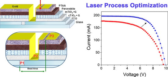
The P3 ablation consists of selective removal of the CE layer, by leaving the underneath layers intact. In our work, thermally evaporated gold thin film constitutes the module CE, with a thickness of 150 nm. In reality, incorrect P3 laser ablation in the form of (i) an excessive amount of energy transfer to the material, (ii) a prolonged laser ablation, can induce local heating, material melting between adjacent cells or incomplete removal of the gold inside the ablated area. In particular, an incomplete gold removal can generate short circuits between two adjacent sub-cell counter electrodes. Sometimes, the presence of few gold flakes in the P3 ablated area could lead to the formation of resistive paths, electrically connecting adjacent cells eventually penalizing electrical characteristics of the module (short circuit current -ISC-, open circuit voltage -VOC-, fill factor -FF-, PCE).
The I-V curves depicted in Figure 4 are acquired under 1SUN illumination using different laser ablation parameters during P3 process. In particular, the red I-V curve is related to a PSM ablated by using a single scribe P3 process with a fluence equal to 254.8 mJ·cm−2, leading to a non-optimized P3 process in terms of incomplete gold removal. However, it is not easy to promptly correlate lowering of PSM performance to the P3 ablation parameters since adjacent cells are not completed shunting. The presence of gold flakes inside the P3 scribes can generate resistive paths characterized by random values starting from few Ω (one or more cells shunted) till KΩ. The latter case can be clearly observed in Figure 4, where the presence of residual gold flakes generating resistive paths among adjacent cells, but not a complete cell short circuit. This resulted in a remarkable ISC (−11.8%) and FF (−18.1%) decrease, while VOC experienced a mild reduction (−3.5%), lower than the one occurring in the case of a complete cell shunting. Thus, with the aim to obtain optimal isolation among adjacent cells, we performed a P3 ablation by a 20% increased laser fluence (306 mJ·cm−2) resulting in the blue I-V curve reported in Figure 4. The module efficiency has been increased up to 15.3%, demonstrating that a not optimized P3 process could compromise the module sub-cell interconnections. Regarding the ISC, we could also observe an improvement of 11.8% (from 176.17 mA to 196.97 mA) by using the optimized P3 parameters. The percentage increase of the module electrical parameters obtained by applying an optimized P3 process in terms of fluence with respect to a non-optimized one is summarized in Table 1.
Module monolithic connections must be able to resist also to the panel lamination process usually inducing additional thermal and mechanical stress. To avoid module PCE drop during panel lamination, presence of spurious gold flakes arising from the ablation process needs to be minimized and sharp edges for sub-cell gold CEs should be guaranteed after P3 process. In order to assess the ablation induced particulate and with the aim to further refine P3 process parameters, a 150 nm thick gold layer was evaporated over a glass substrate and subsequently patterned with P3 parameters. The residual gold flakes present on the substrate after the laser process were analyzed by optical microscopy.
Despite several studies [3,46,47,48] demonstrated the possibility to achieve high module aperture ratio performing very narrow P3 ablations (less than 15 µm), Figure 5a shows how gold flakes can generate short circuit using a single 12 µm width P3 scribe. The scribe reported in Figure 5a shows that a pulse fluence of 221.2 mJ·cm−2 was not able to achieve a full electrical separation among adjacent gold regions. In fact, the unremoved portion of gold layer is still visible after the P3 ablation (see red circles in Figure 5a), creating a conductive path of about 60 µm length. Considering a gold thickness of 150 nm, we can estimate a resistance value of about 6 Ω for such kind of conductive path. Within the entire P3 scribe length (11 cm), we could find several similar conductive paths, electrically in parallel with each other. This means that the detectable equivalent resistance between two counter electrodes can have a value starting from a few Ω up to a few hundred Ω, depending on number, size, and adhesion strength of residual gold flakes forming conductive paths. Increasing the fluence value up to 306 mJ·cm−2, the presence of gold flakes is significantly reduced (Figure 5b), but there is still a non-negligible risk of creating short circuits and parasitic resistive connections during the module lamination step, due to the presence of flakes larger than 4 µm inside a scribe of 13.5 µm. Complete electrical isolation with a negligible residual presence of gold flakes can be achieved by using fluence values higher than 354 mJ·cm−2 (Figure 5c), but unfortunately, in this case, laser-induced damages on the underneath glass. Alternatively, to the single scribe process, a multi-scribe process with reduced laser fluence can be implemented to achieve optimal electrical insulation and to avoid substrate damages by minimizing the residual gold flakes. Figure 5d show multi-scribe P3 ablations employing RSD equal to 3 µm and a pulse fluence equal to 306 mJ·cm−2. In this case, ablation width equal to 130 µm is obtained by leaving on the substrate only a few flakes with a diameter lower than 5 µm. Finally, the optimized parameters were tested in PSM fabrication and microscope images of P3 process are reported in Figure 6.
This test confirmed our previous results revealing an incomplete gold removal (Figure 6a) when a 221.2 mJ·cm−2 pulse fluence is used, leaving electrical bridges between module constituting sub-cells that could eventually reduce the module PCE. On the opposite, a pulse fluence up to 354 mJ·cm−2 led to excessive stress on the layer during the laser process, inducing layer delamination and irreversibly damaging the underneath FTO layer (Figure 6b). The gold CE delamination should be carefully avoided since it induces a remarkable reduction in sub-cell active areas and eventually an unbalance in sub-cell current across the module. Moreover, the potential detachment of large gold flakes can increase the occurrence of short-circuits during the module lamination process. The best result is achieved by using a pulse fluence of 306 mJ·cm−2 as shown in Figure 6c, characterized by negligible residual flakes and no layer delamination from the sharp edges of the ablated area.
We should point out that a 12 µm P3 ablation width can impact module characteristics during the manufacturing processes related to the panel lamination even though the as-fabricated electrical characteristics seem to be good enough. In fact, modules composing panel strings have to be encapsulated, electrically connected (series and/or parallel connection depending on the desired panel output), and finally laminated (front glass-rear glass or front glass-back plastic/aluminum foil). More in detail, the lamination process is usually carried out in vacuum by applying an optimized pressure over the stack front-glass/EVA/PSMs/EVA/back-sheet (or rear glass) [49,50] that could induce undesired cell shunts in PSMs in case of incomplete gold removal. This undesired effect, imputed to the roughness of the underneath layer stack, can be detrimental during the lamination process, where the applied pressure (105 Pa) [51] could reconnect two or more sub-cell CEs [52,53], as reported in Figure 7.
The microscope images reported in Figure 7 is referring to a 12 µm P3 scribe able to guarantee full electrical isolation between two adjacent gold CEs. However, residual flakes with dimensions comparable to the P3 scribe width could reconnect two adjacent cells (Figure 7b) upon the application of external pressure. In order to elucidate how this phenomenon can impact over a real PSM performance, a PSM employing a P3 width of 12 µm was measured immediately after the laser ablation (triangle symbols - blue I-V curve reported in Figure 8a) and after a subsequent application (from the CE side) of a pressure comparable to those employed during the lamination process (square symbols - red I-V curve in Figure 8a).
A clear VOC (−12.8%) and FF (−20.2%) reduction was observed after the application of the external pressure, testifying to the detrimental effect of the gold residual flakes among adjacent cells. Remarkably, the final PCE (10.45%) was 31.7% lower than the value measured before the lamination process. All the electrical module characteristics before and after the application of the lamination pressure and the relative variations are summarized in Table 2. This detrimental effect is not occurring by using a P3 ablation width of 130 µm, as shown in the I-V curves reported in Figure 8b.
The parameter sets optimized for each laser process (P1, P2, P3) employed in the PSM fabrication are summarized in Table 3, by detailing the fluence (mJ·cm−2), laser power, PRR, translation speed (cm/s−1) and RSD (μm).
Finally, in Figure 9, we reported the electrical parameters for 4 as-realized modules extracted from the I-V curves acquired before and after the application of a pressure comparable to that employed in a standard lamination process (≈1 Atm). Notably, besides the minor variations due to the production process between the modules, the use of an optimized P3 process guaranteed stable electrical performance before and after the external pressure application, by demonstrating the robustness of the proposed fabrication process for 2D-PSMs.
4. Conclusions
In order to gain the attention of the industrial world, perovskite solar cell technology should demonstrate the reproducibility and reliability of high-throughput production processes for large-area modules. Laser is commonly recognized as the first choice for ablation processes, usually employed for realizing monolithically integrated cell interconnections in thin-film photovoltaic technologies. In this work, we successfully optimized the P2 and P3 ablation processes by demonstrating excellent performance for 2D-material engineered perovskite solar modules, with PCE exceeding 15% over 83 cm2 active area. On one side, the optimized set of P2 laser ablation parameters (laser fluence (248.8 mJ·cm−2), RSD (2 µm) and PRR (80 kHz)) allowed to effectively remove the 2D material based ETL/perovskite/HTL stack from the FTO interconnection area, by ensuring the minimum impact of vertical sub-cell interconnections onto the module series resistance. On the other side, a 130 nm width, well-defined and gold-residual-free P3 ablation (achieved with laser pulse fluence of 306 mJ·cm−2, RSD equal to 3 µm) resulted in high-performance modules able to pass without significant PCE losses, the stressful conditions dictated by the module lamination process employed for panel production. The module fabrication process proposed here represents a viable route for pushing the industrialization of perovskite photovoltaic technology.
Author Contributions
Conceptualization, S.R., S.P., A.A., and A.D.C.; data curation, S.P., A.A., and A.D.C.; formal analysis, S.R., S.P., A.A., and A.D.C.; funding acquisition, A.D.C.; investigation, S.R., S.P., A.A., and A.D.C.; methodology, S.R., S.P., and A.A.; project administration, A.D.C.; resources, A.D.C.; supervision, S.P., A.A., and A.D.C.; validation, S.P., A.A., and A.D.C.; visualization, S.P. and A.A.; writing—original draft, S.R., S.P., and A.A.; writing—review and editing, S.R., S.P., A.A., and A.D.C. All authors have read and agreed to the published version of the manuscript.
Funding
This Project has received funding from the European Union’s Horizon 2020 research and innovation program under Grant Agreement GrapheneCore3 N° 881603. A.D.C. gratefully acknowledges the financial support from the Ministry of Education and Science of the Russian Federation in the framework of MegaGrant (no. 075-15-2019-872 (14.Y26.31.0027/074-02-2018-327)).
Informed Consent Statement
Not applicable.
Data Availability Statement
Data is contained within the article.
Conflicts of Interest
The authors declare no conflict of interest.
References
- Efficiency-Chart. Available online: https://www.nrel.gov/pv/assets/images/efficiency-chart.png (accessed on 27 December 2020).
- Lamanna, E.; Matteocci, F.; Calabro, E.; Serenelli, L.; Salza, E.; Martini, L.; Menchini, F.; Izzi, M.; Agresti, A.; Pescetelli, S.; et al. Mechanically Stacked, Two-Terminal Graphene-Based Perovskite/Silicon Tandem Solar Cell with Efficiency over 26%. Joule 2020, 4, 865–881. [Google Scholar] [CrossRef]
- Lee, S.W.; Bae, S.; Kim, D.; Lee, H.S. Historical Analysis of High-Efficiency, Large-Area Solar Cells: Toward Upscaling of Perovskite Solar Cells. Adv. Mater. 2020, 32, 2002202. [Google Scholar] [CrossRef]
- Yoon, J.H.; Park, J.K.; Kim, W.M.; Lee, J.; Pak, H.; Jeong, J.H. Characterization of efficiency-limiting resistance losses in monolithically integrated Cu(In,Ga)Se 2 solar modules. Sci. Rep. 2015, 5, 7690. [Google Scholar] [CrossRef] [Green Version]
- Li, Z.; Klein, T.R.; Kim, D.H.; Yang, M.; Berry, J.J.; Van Hest, M.F.A.M.; Zhu, K. Scalable fabrication of perovskite solar cells. Nat. Rev. Mater. 2018, 3, 18017. [Google Scholar] [CrossRef]
- Stolterfoht, M.; Caprioglio, P.; Wolff, C.M.; Márquez, J.A.; Nordmann, J.; Zhang, S.; Rothhardt, D.; Hörmann, U.; Amir, Y.; Redinger, A.; et al. The impact of energy alignment and interfacial recombination on the internal and external open-circuit voltage of perovskite solar cells. Energy Environ. Sci. 2019, 12, 2778–2788. [Google Scholar] [CrossRef] [Green Version]
- Zhao, Z.; Li, Q.; Gong, J.; Li, Z.; Zhang, J. Challenges and Approaches Towards Upscaling Assembly of Hybrid Perovskite Solar Cells. Mater. Adv. 2020, 1, 292–309. [Google Scholar] [CrossRef]
- Mariani, P.; Agresti, A.; Vesce, L.; Pescetelli, S.; Palma, A.L.; Tomarchio, F.; Karagiannidis, P.; Ferrari, A.; Di Carlo, A. Graphene-based interconnections for solar modules sensitized to stable dyes. ACS Appl. Energy Mater. 2021, 4, 98–110. [Google Scholar] [CrossRef]
- Palma, A.L. Laser-Processed Perovskite Solar Cells and Modules. Sol. RRL 2020, 4, 1900432. [Google Scholar] [CrossRef]
- Galagan, Y. Stability of perovskite PV modules. J. Phys. Energy 2020, 2, 021004. [Google Scholar] [CrossRef]
- Zeng, L.; Chenb, S.; Forberichc, K.; Brabecd, C.J.; Maia, Y.; Guoa, F. Environmental Science. Energy Environ. Sci. 2020, 13, 4666–4690. [Google Scholar] [CrossRef]
- Chen, X.; Cheng, S.; Xiao, L.; Sun, H. Identifying, understanding and controlling defects and traps in halide perovskites for optoelectronic devices: A review. J. Phys. D Appl. Phys. 2020, 53, 373001. [Google Scholar] [CrossRef]
- Acik, M.; Darling, S.B. Graphene in perovskite solar cells: Device design, characterization and implementation. J. Mater. Chem. A 2016, 4, 6185–6235. [Google Scholar] [CrossRef]
- Su, H.; Wu, T.; Cui, D.; Lin, X.; Luo, X.; Wang, Y.; Han, L. The Application of Graphene Derivatives in Perovskite Solar Cells. Small Methods 2020, 4, 2000507. [Google Scholar] [CrossRef]
- Kakavelakis, G.; Gouda, L.; Tischler, Y.; Kaliakatsos, I.; Petridis, K. 2D Transition Metal Dichalcogenides for Solution-Processed Organic and Perovskite Solar Cells. In Two Dimensional Transition Metal Dichalcogenides: Synthesis, Properties, and Applications; Arul, N.S., Nithya, V.D., Eds.; Springer: Singapore, 2019; pp. 203–239. ISBN 978-981-13-9045-6. [Google Scholar]
- Agresti, A.; Pazniak, A.; Pescetelli, S.; Di Vito, A.; Rossi, D.; Pecchia, A.; Auf der Maur, M.; Liedl, A.; Larciprete, R.; Kuznetsov, D.V.; et al. Titanium-carbide MXenes for work function and interface engineering in perovskite solar cells. Nat. Mater. 2019, 18, 1228–1234. [Google Scholar] [CrossRef] [PubMed] [Green Version]
- Saranin, D.; Pescetelli, S.; Pazniak, A.; Rossi, D.; Liedl, A.; Yakusheva, A.; Luchnikov, L.; Podgorny, D.; Gostischev, P.; Didenko, S.; et al. Transition metal carbides (MXenes) for efficient NiO-based inverted perovskite solar cells. Nano Energy 2021, 82, 105771. [Google Scholar] [CrossRef]
- Seitz, M.; Gant, P.; Castellanos-Gomez, A.; Prins, F. Long-term stabilization of two-dimensional perovskites by encapsulation with hexagonal boron nitride. Nanomaterials 2019, 9, 1120. [Google Scholar] [CrossRef] [Green Version]
- Zhang, F.; He, J.; Xiang, Y.; Zheng, K.; Xue, B.; Ye, S.; Peng, X.; Hao, Y.; Lian, J.; Zeng, P.; et al. Semimetal–Semiconductor Transitions for Monolayer Antimonene Nanosheets and Their Application in Perovskite Solar Cells. Adv. Mater. 2018, 30, 1803244. [Google Scholar] [CrossRef]
- Di Carlo, A.; Agresti, A.; Brunetti, F.; Pescetelli, S. Two-dimensional materials in perovskite solar cells. J. Phys. Energy 2020, 2, 031003. [Google Scholar] [CrossRef]
- You, P.; Tang, G.; Yan, F. Two-dimensional materials in perovskite solar cells. Mater. Today Energy 2019, 11, 128–158. [Google Scholar] [CrossRef]
- Bati, A.S.R.; Batmunkh, M.; Shapter, J.G. Emerging 2D Layered Materials for Perovskite Solar Cells. Adv. Energy Mater. 2019, 10, 1902253. [Google Scholar] [CrossRef]
- Ma, J.Y.; Sun, M.; Zhu, Y.; Zhou, H.; Wu, K.; Xiao, J.; Wu, M. Highly Effective 2D Layer Structured Titanium Carbide Electrode for Dye-Sensitized and Perovskite Solar Cells. ChemElectroChem 2020, 7, 1149–1154. [Google Scholar] [CrossRef]
- Zhou, J.; Ren, Z.; Li, S.; Liang, Z.; Surya, C.; Shen, H. Semi-transparent Cl-doped perovskite solar cells with graphene electrodes for tandem application. Mater. Lett. 2018, 220, 82–85. [Google Scholar] [CrossRef]
- Tai, Q.; Yan, F. Emerging Semitransparent Solar Cells: Materials and Device Design. Adv. Mater. 2017, 29, 1700192. [Google Scholar] [CrossRef]
- Sung, H.; Ahn, N.; Jang, M.S.; Lee, J.K.; Yoon, H.; Park, N.G.; Choi, M. Transparent Conductive Oxide-Free Graphene-Based Perovskite Solar Cells with over 17% Efficiency. Adv. Energy Mater. 2016, 6, 2–7. [Google Scholar] [CrossRef]
- Tran, V.D.; Pammi, S.V.N.; Park, B.J.; Han, Y.; Jeon, C.; Yoon, S.G. Transfer-free graphene electrodes for super-flexible and semi-transparent perovskite solar cells fabricated under ambient air. Nano Energy 2019, 65, 104018. [Google Scholar] [CrossRef]
- Chen, B.; Zheng, X.; Bai, Y.; Padture, N.P.; Huang, J. Progress in Tandem Solar Cells Based on Hybrid Organic–Inorganic Perovskites. Adv. Energy Mater. 2017, 7, 1602400. [Google Scholar] [CrossRef]
- Lang, F.; Gluba, M.A.; Albrecht, S.; Rappich, J.; Korte, L.; Rech, B.; Nickel, N.H.; Lang, F.; Gluba, M.A.; Albrecht, S.; et al. Perovskite Solar Cells with Large-Area CVD-Graphene for Tandem Solar Cells Perovskite Solar Cells with Large-Area CVD-Graphene for Tandem Solar Cells. J. Phys. Chem. Lett. 2015, 6, 2745–2750. [Google Scholar] [CrossRef] [Green Version]
- Petridis, C.; Kakavelakis, G.; Kymakis, E. Renaissance of graphene-related materials in photovoltaics due to the emergence of metal halide perovskite solar cells. Energy Environ. Sci. 2018, 11, 1030–1061. [Google Scholar] [CrossRef]
- Agresti, A.; Pescetelli, S.; Palma, A.L.; Martin-Garcia, B.; Najafi, L.; Bellani, S.; Moreels, I.; Prato, M.; Bonaccorso, F.; Di Carlo, A. Two-dimensional (2D) Material Interface Engineering for Efficient Perovskite Large-area Modules. ACS Energy Lett. 2019, 4, 1862–1871. [Google Scholar] [CrossRef]
- Biccari, F.; Gabelloni, F.; Burzi, E.; Gurioli, M.; Pescetelli, S.; Agresti, A.; Del Rio Castillo, A.E.; Ansaldo, A.; Kymakis, E.; Bonaccorso, F.; et al. Graphene-Based Electron Transport Layers in Perovskite Solar Cells: A Step-Up for an Efficient Carrier Collection. Adv. Energy Mater. 2017, 7, 1701349. [Google Scholar] [CrossRef]
- Taheri, B.; Nia, N.Y.; Agresti, A.; Pescetelli, S.; Ciceroni, C.; Del Rio Castillo, A.E.; Cinà, L.; Bellani, S.; Bonaccorso, F.; Di Carlo, A. Graphene-engineered automated sprayed mesoscopic structure for perovskite device scaling-up. 2D Mater. 2018, 5, 045034. [Google Scholar] [CrossRef]
- O’Keeffe, P.; Catone, D.; Paladini, A.; Toschi, F.; Turchini, S.; Avaldi, L.; Martelli, F.; Agresti, A.; Pescetelli, S.; Del Rio Castillo, A.E.; et al. Graphene-Induced Improvements of Perovskite Solar Cell Stability: Effects on Hot-Carriers. Nano Lett. 2019, 19, 684–691. [Google Scholar] [CrossRef]
- Wang, B.; Iocozzia, J.; Zhang, M.; Ye, M.; Yan, S.; Jin, H.; Wang, S.; Zou, Z.; Lin, Z. The charge carrier dynamics, efficiency and stability of two-dimensional material-based perovskite solar cells. Chem. Soc. Rev. 2019, 48, 4854–4891. [Google Scholar] [CrossRef] [PubMed]
- Pescetelli, S.; Castriotta, L.A.; Agresti, A.; Di Carlo, A. Large area perovskite solar modules with improved efficiency and stability. In Proceedings of the 2019 International Symposium on Advanced Electrical and Communication Technologies (ISAECT), Rome, Italy, 27–29 November 2019; pp. 1–5. [Google Scholar]
- Agresti, A.; Pescetelli, S.; Taheri, B.; Del Rio Castillo, A.E.; Cinà, L.; Bonaccorso, F.; Di Carlo, A. Graphene-Perovskite Solar Cells Exceed 18% Efficiency: A Stability Study. ChemSusChem 2016, 9, 2609–2619. [Google Scholar] [CrossRef]
- Polyakov, A.Y.; Smirnov, N.B.; Shchemerov, I.V.; Saranin, D.S.; Le, T.S.; Didenko, S.I.; Kuznetsov, D.V.; Agresti, A.; Pescetelli, S.; Matteocci, F.; et al. Trap states in multication mesoscopic perovskite solar cells: A deep levels transient spectroscopy investigation. Appl. Phys. Lett. 2018, 113, 263501. [Google Scholar] [CrossRef]
- Noël, C.; Pescetelli, S.; Agresti, A.; Franquet, A.; Spampinato, V.; Felten, A.; di Carlo, A.; Houssiau, L.; Busby, Y. Hybrid perovskites depth profiling with variable-size argon clusters and monatomic ions beams. Materials 2019, 12, 726. [Google Scholar] [CrossRef] [Green Version]
- Agresti, A.; Berionni Berna, B.; Pescetelli, S.; Catini, A.; Menchini, F.; Di Natale, C.; Paolesse, R.; Di Carlo, A. Copper-Based Corrole as Thermally Stable Hole Transporting Material for Perovskite Photovoltaics. Adv. Funct. Mater. 2020, 30, 2003790. [Google Scholar] [CrossRef]
- Yadav, S.K.; Ravishankar, S.; Pescetelli, S.; Fabregat-santiago, F.; Di Carlo, A.; Agresti, A. Stability of dye-sensitized solar cells under extended thermal stress. Phys. Chem. Chem. Phys. 2017, 19, 22546–22554. [Google Scholar] [CrossRef]
- Zanotti, G.; Angelini, N.; Mattioli, G.; Paoletti, A.M.; Pennesi, G.; Caschera, D.; Sobolev, A.P.; Beverina, L.; Calascibetta, A.M.; Sanzone, A.; et al. [1]Benzothieno[3,2-b][1]benzothiophene-Phthalocyanine Derivatives: A Subclass of Solution-Processable Electron-Rich Hole Transport Materials. Chempluschem 2020, 85, 2376–2386. [Google Scholar] [CrossRef] [PubMed]
- Agresti, A.; Pescetelli, S.; Gatto, E.; Venanzi, M.; Di Carlo, A. Polyiodides formation in solvent based Dye Sensitized Solar Cells under reverse bias stress. J. Power Sources 2015, 287, 87–95. [Google Scholar] [CrossRef]
- Werner, J.; Boyd, C.C.; Moot, T.; Wolf, E.J.; France, R.M.; Johnson, S.A.; van Hest, M.F.A.M.; Luther, J.M.; Zhu, K.; Berry, J.J.; et al. Learning from existing photovoltaic technologies to identify alternative perovskite module designs. Energy Environ. Sci. 2020, 13, 3393–3403. [Google Scholar] [CrossRef]
- Matteocci, F.; Razza, S.; Di Giacomo, F.; Casaluci, S.; Mincuzzi, G.; Brown, T.M.; D’Epifanio, A.; Licoccia, S.; Di Carlo, A. Solid-state solar modules based on mesoscopic organometal halide perovskite: A route towards the up-scaling process. Phys. Chem. Chem. Phys. 2014, 16, 3918–3923. [Google Scholar] [CrossRef] [PubMed]
- Palma, A.L.; Matteocci, F.; Agresti, A.; Pescetelli, S.; Calabro, E.; Vesce, L.; Christiansen, S.; Schmidt, M.; Di Carlo, A. Laser-Patterning Engineering for Perovskite Solar Modules With 95% Aperture Ratio. IEEE J. Photovolt. 2017, 7, 1674–1680. [Google Scholar] [CrossRef]
- Galagan, Y.; Coenen, E.W.C.; Verhees, W.; Andriessen, R. Towards scaling up of perovskite solar cells and modules. J. Mater. Chem. A 2016, 4, 5700–5705. [Google Scholar] [CrossRef]
- Yang, M.; Kim, D.H.; Klein, T.R.; Li, Z.; Reese, M.O.; De Tremolet Villers, B.J.; Berry, J.J.; Van Hest, M.F.A.M.; Zhu, K. Highly Efficient Perovskite Solar Modules by Scalable Fabrication and Interconnection Optimization. ACS Energy Lett. 2018, 3, 322–328. [Google Scholar] [CrossRef]
- El Amrani, A.; Mahrane, A.; Moussa, F.Y.; Boukennous, Y. Solar Module Fabrication. Int. J. Photoenergy 2007, 2007, 027610. [Google Scholar] [CrossRef]
- Nyarko, F.K.A.; Takyi, G.; Amalu, E.H. Robust crystalline silicon photovoltaic module ( c-Si PVM ) for the tropical climate: Future facing the technology. Sci. Afr. 2020, 8, e00359. [Google Scholar] [CrossRef]
- Tippabhotla, S.K.; Radchenko, I.; Song, W.J.R.; Illya, G.; Budiman, A.S. From cells to laminate: Probing and modeling residual stress evolution in thin silicon photovoltaic modules using synchrotron X-ray micro-diffraction experiments and fi nite element simulations. Prog. Photovolt. Res. Appl. 2017, 25, 791–809. [Google Scholar] [CrossRef] [Green Version]
- Kubis, P.; Li, N.; Stubhan, T.; Machui, F.; Matt, G.J.; Voigt, M.M.; Brabec, C.J. Patterning of organic photovoltaic modules by ultrafast laser. Prog. Photovolt. Res. Appl. 2013, 23, 238–246. [Google Scholar] [CrossRef]
- Qiu, L.; He, S.; Ono, L.K.; Liu, S.; Qi, Y. Scalable Fabrication of Metal Halide Perovskite Solar Cells and Modules. ACS Energy Lett. 2019, 4, 2147–2167. [Google Scholar] [CrossRef]
Figure 1.
A schematic representation of P1, P2, P3 laser processes: (a) P1 laser process for electrical isolation of the 9 sub-cell photoelectrodes composing the module; (b) P2b: Printing of metal mask for cTiO2 patterning; (c) P2b: cTiO2 deposition by spray pyrolysis; (d) P2b: metal mask chemical lift-off; (e) deposition of all the layers composing the module; (f) P2b laser process for removing all the layers composing the module from the fluorinated tin-oxide (FTO) areas used to electrically connect the module sub-cells; (g) Au thermal evaporation all over the module surface; (h) P3 laser process for module sub-cells counter electrodes (CEs) electrical separation; (i) total dead area and final module layout.
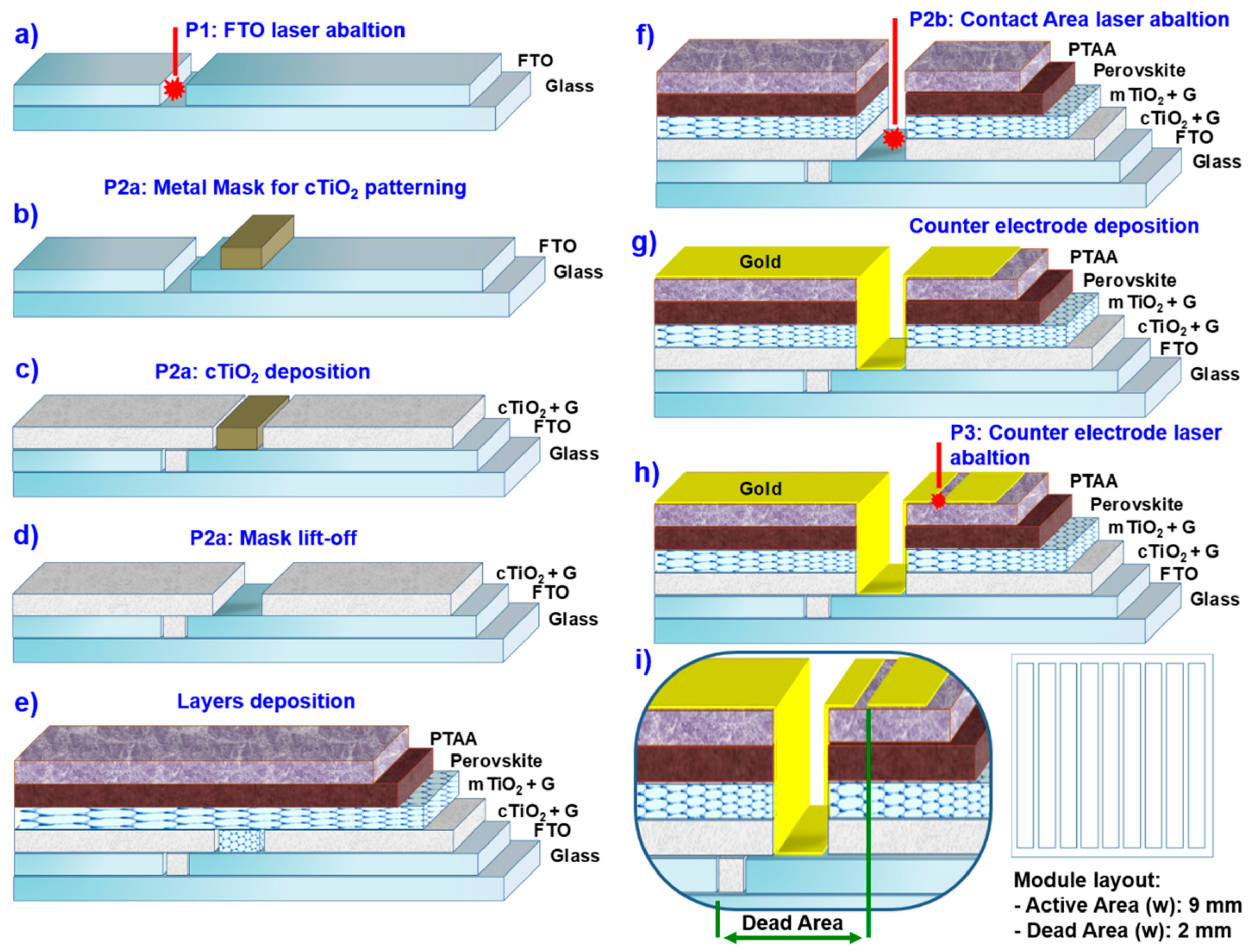
Figure 2.
Ablated area obtained by 2-step P2 laser ablation over mTiO2+G/perovskite/PTAA stack.
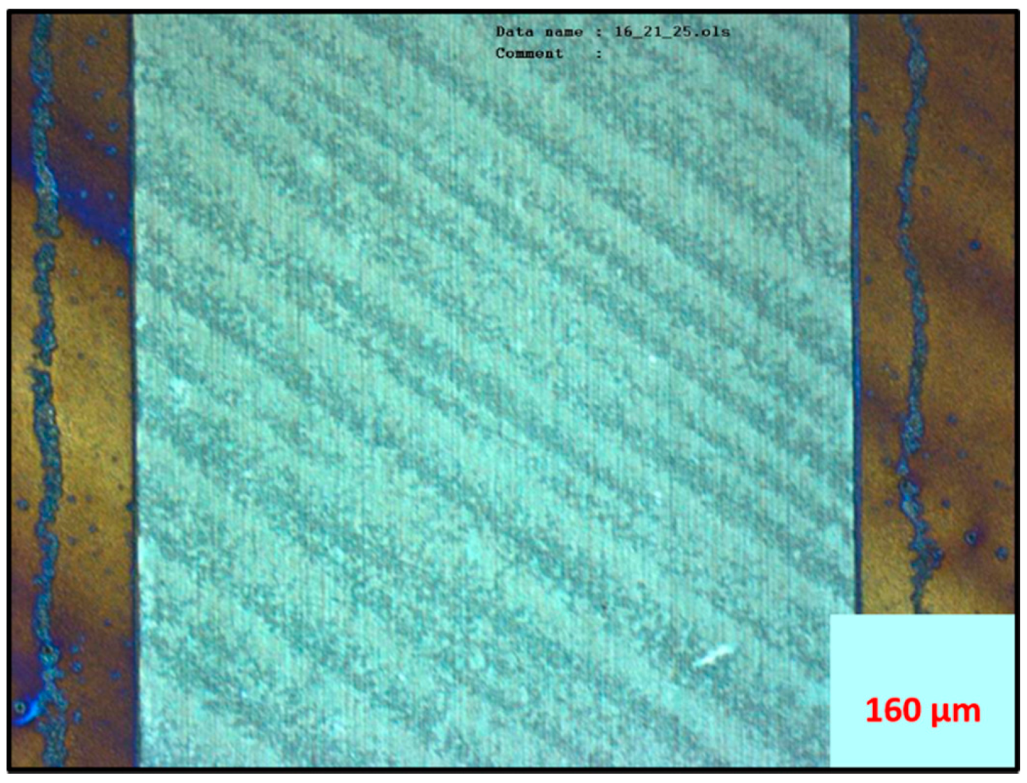
Figure 3.
Effects induced by laser radiation on FTO layer, after a P2 process repeated 2 times (raster scanning distance (RSD) = 2 µm) and by employing a laser fluence ranging from 220 mJ·cm−2 to 360 mJ·cm−2. A clear FTO damage is induced by a laser fluence value starting from 300 mJ·cm−2, till to the complete FTO removal at 360 mJ·cm−2.
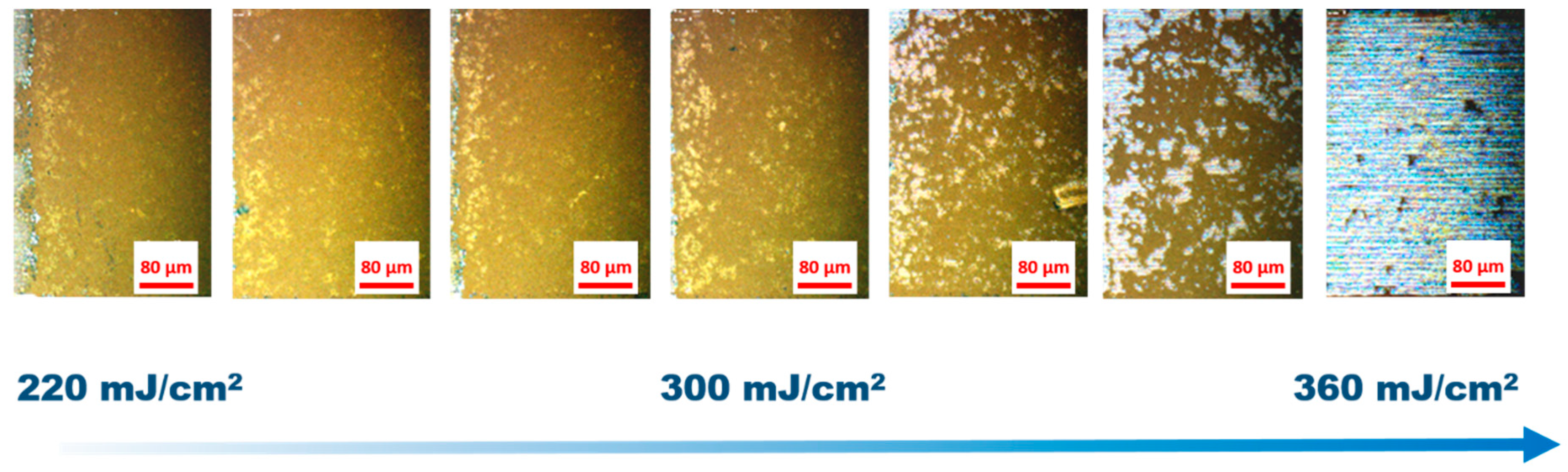
Figure 4.
P3 parameter optimization and the relative I-V curves for the as-realized modules. In particular, module realized employing a non-optimized laser fluence (254.8 mJ·cm−2) during P3 (square symbols—red line) demonstrated power conversion efficiency (PCE) of 11.23% while module realized employing an optimized laser fluence (306 mJ·cm−2) showed PCE up to 15.29% (triangle symbols—blue line). The reported I-V curves were acquired under 1 SUN illumination.
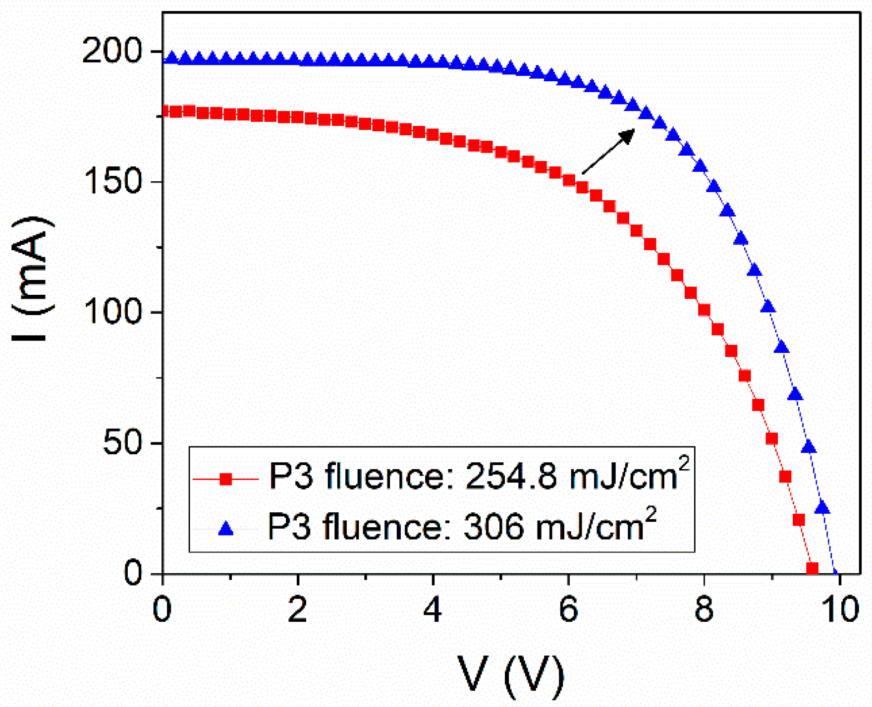
Figure 5.
Optical images for 150 nm thick gold layer evaporated over a glass substrate to test the gold removal during P3 by employing 4 different scribing processes: (a) single laser process employing a pulse fluence of 221.2 mJ·cm−2 and resulting in 12 µm width scribe; (b) single laser process employing a pulse fluence of 306 mJ·cm−2 and resulting in 13.5 µm width scribe; (c) single laser process employing a pulse fluence of 354 mJ·cm−2 and resulting in 15 µm width scribe; (d) ablated area in the case of a 130 µm width scribe obtained by using a raster scanning distance of 3 µm and a pulse fluence of 306 mJ·cm−2.
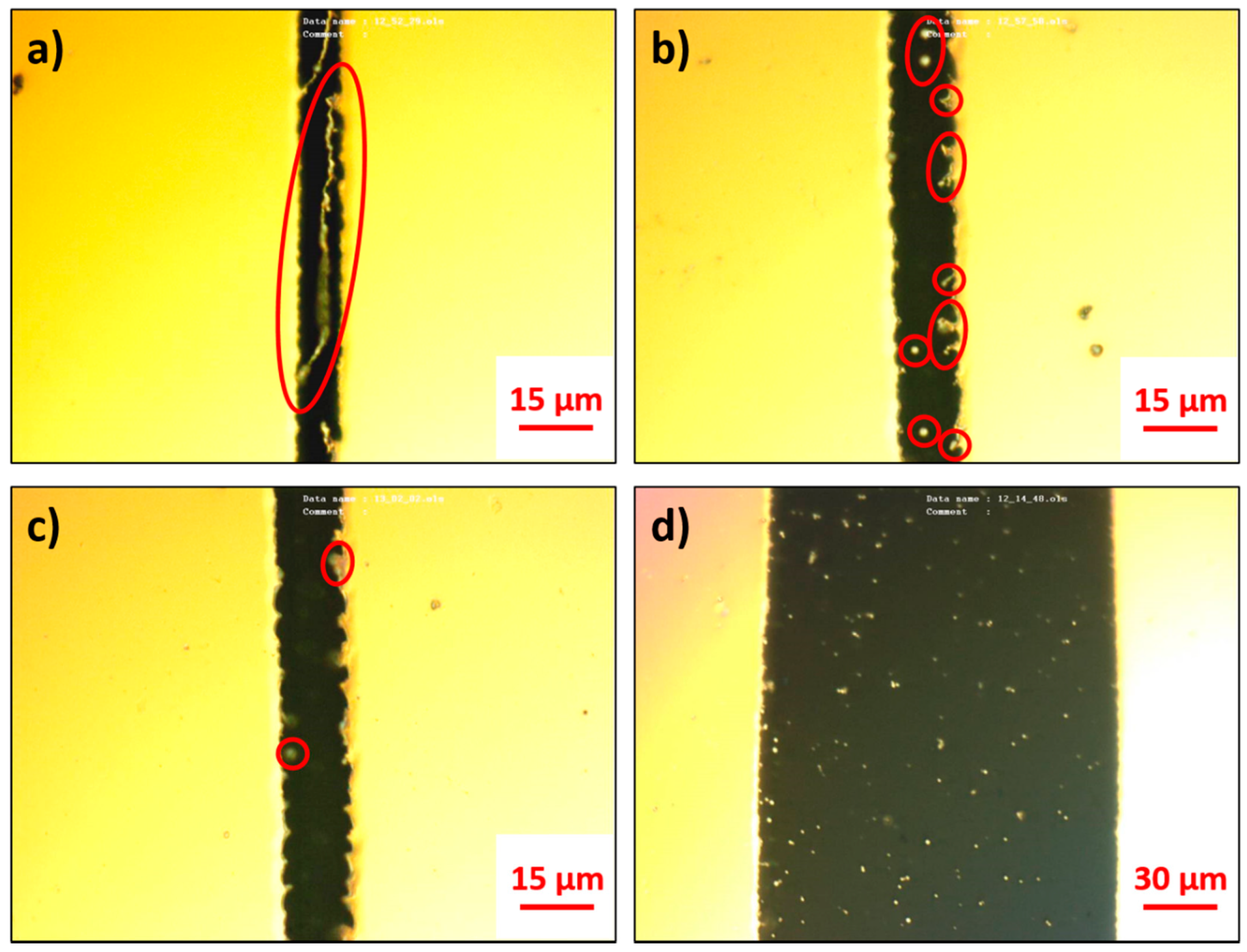
Figure 6.
P3 laser ablation microscope analysis: (a) Optical image for a 130 µm width P3 scribe obtained by using a RSD of 3 µm and a pulse fluence value of 221.2 mJ·cm−2. In this case, the presence of electrical bridges between module constituting sub-cells due to an incomplete gold removal is clearly visible; (b) Optical image for a 130 µm width P3 scribe obtained by using a RSD of 3 µm and a pulse fluence value of 354 mJ·cm−2. In this case, the layer delamination on the edge of the ablated area is due to excessive stress experienced by the gold film during the P3 ablation; (c) Optical image for a 130 µm width P3 scribe obtained by using a RSD of 3 µm and a pulse fluence value of 306 mJ·cm−2. The as-optimized P3 ablation resulted in an ablated area with negligible gold residual flakes and sharp edges without layer delamination.
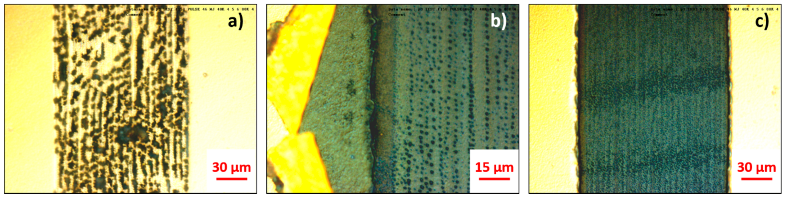
Figure 7.
Single P3 laser scribe (12 µm width), panel (a) points out residual gold flakes with dimensions comparable to the scribe width (b) magnification of the residual gold flakes region along the P3 scribe (green rectangle in panel (a)), by emphasizing a possible shunting mechanism occurring upon the application of an external pressure, commonly employed during the panel lamination process.
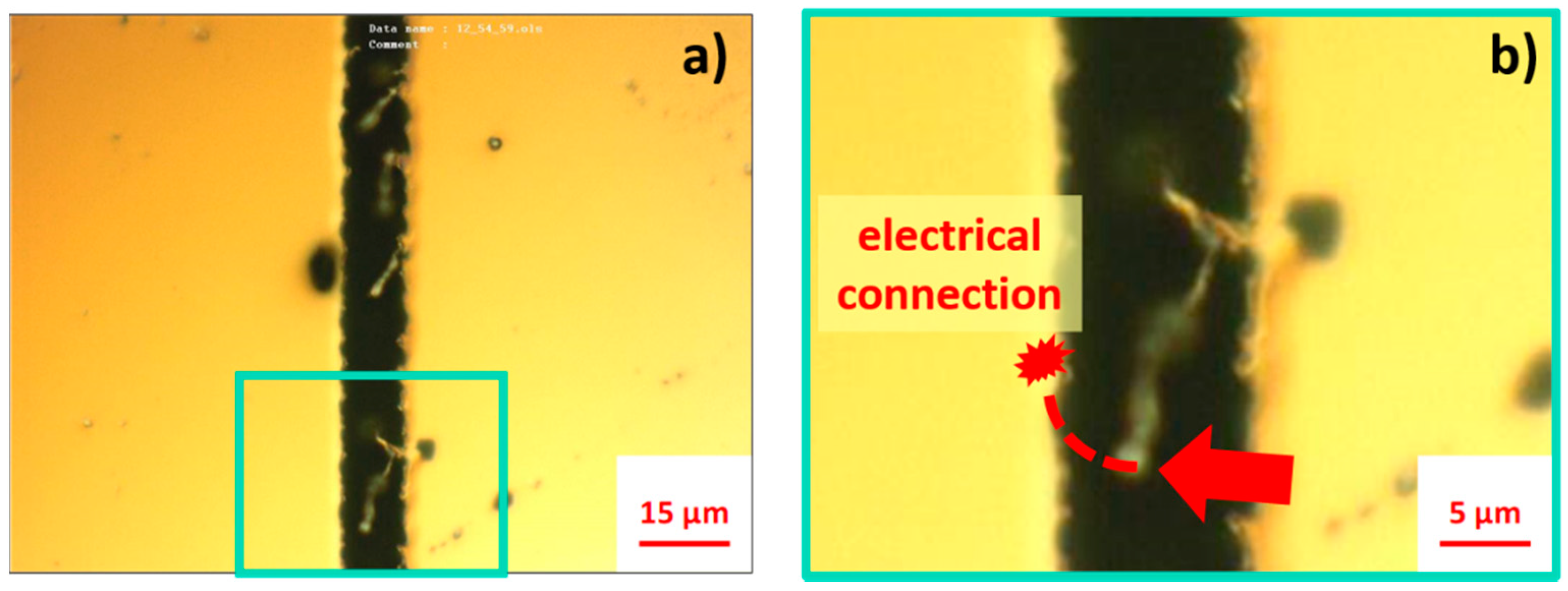
Figure 8.
Module I-V curves, in panel (a) are reported for a module obtained with a non-optimized P3 process before and after the application of the lamination pressure showing a reduction in PCE from 15.3% to 10.45%; (b) the same but with a P3 ablated area of 130 µm.
Figure 8.
Module I-V curves, in panel (a) are reported for a module obtained with a non-optimized P3 process before and after the application of the lamination pressure showing a reduction in PCE from 15.3% to 10.45%; (b) the same but with a P3 ablated area of 130 µm.
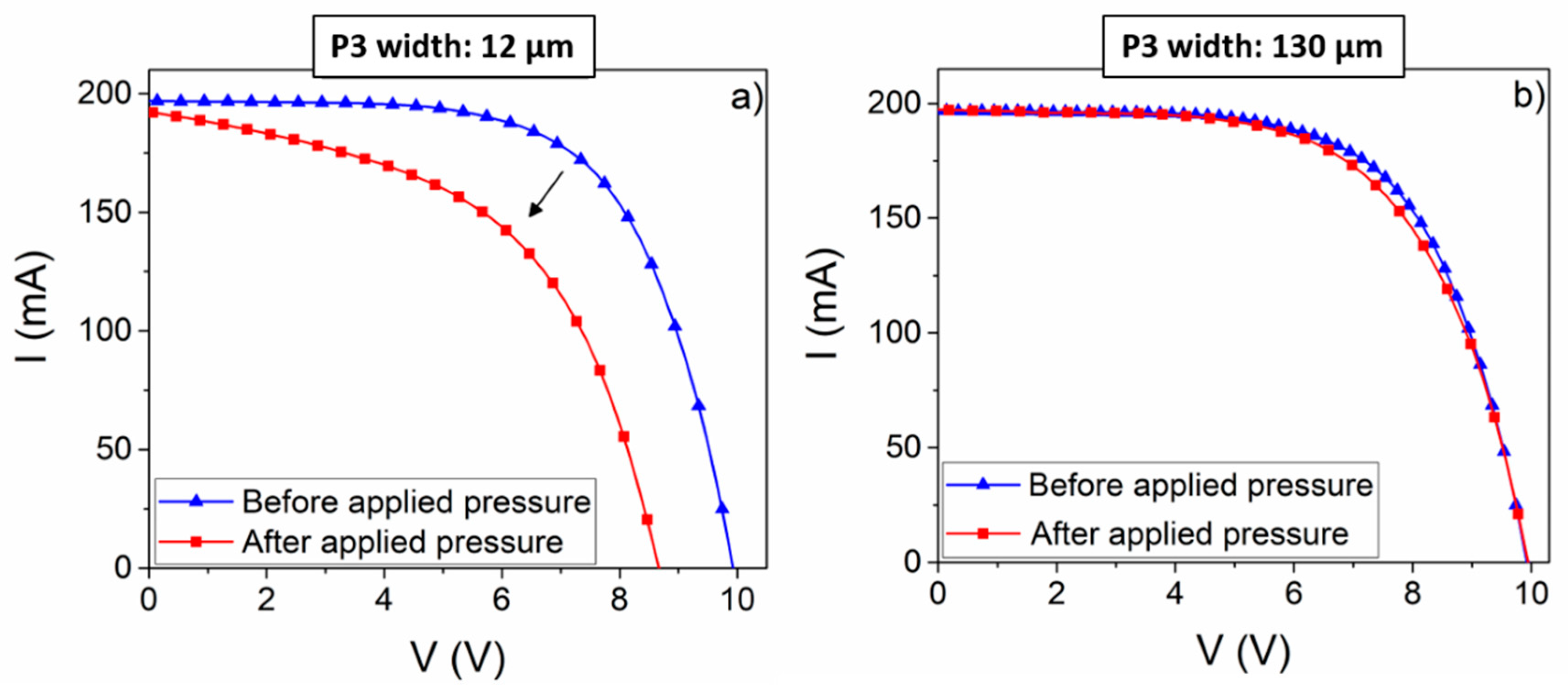
Figure 9.
Electrical parameters related to 4 modules, realized by employing the optimized P3 process and extracted by the I-V curve acquired before (full symbols) and after (empty symbols) the applied pressure, miming the pressure experienced during a standard lamination process.(a) open-circuit voltage VOC; (b) short-circuit current density JSC; (c) fill factor FF and (d) power conversion efficiency PCE.


Table 1.
Electrical parameters (extracted from 1 SUN I-V curves) for modules realized by employing non-optimized (first row) and optimized (second row) laser fluence value during P3 ablation step. The optimized removal of gold layer led to an increased module current and PCE, due to full electrical isolation of the module sub-cells from the counter electrode (CE) side.
| Laser Process | Vmpp (V) | Impp (mA) | Pmpp (mW) | VOC (V) | ISC (mA) | FF (%) | PCE (%) | Laser Fluence (mJ·cm−2) |
|---|---|---|---|---|---|---|---|---|
| Not optimized P3 | 6.60 | 140.69 | 928 | 9.6 | 176.17 | 54.89 | 11.23 | 254.8 |
| Optimized P3 | 7.54 | 167.68 | 1264 | 9.94 | 196.97 | 64.81 | 15.3 | 306 |
| Increment | 14.2% | 19.2% | 36.2% | 3.5% | 11.8% | 18.1% | 36.2% | 20.0% |
Table 2.
Electrical parameters for module produced by using a non-optimized P3 process, extracted by I-V curves acquired (reported in Figure 8a) before and after the application of the lamination pressure, and their relative variations in percentage.
Table 2.
Electrical parameters for module produced by using a non-optimized P3 process, extracted by I-V curves acquired (reported in Figure 8a) before and after the application of the lamination pressure, and their relative variations in percentage.
| Pressure Application | Vmpp (V) | Impp (mA) | Pmpp (mW) | VOC (V) | ISC (mA) | FF (%) | PCE (%) |
|---|---|---|---|---|---|---|---|
| Before pressure | 7.54 | 167.68 | 1264 | 9.94 | 196.97 | 64.81 | 15.3 |
| After pressure | 6.070 | 142.37 | 863.72 | 8.67 | 192.79 | 51.69 | 10.45 |
| Decrement | −18.3% | −15.1% | −31.6% | −12.8% | −1.97% | −20.2% | −31.7% |
Table 3.
Parameter sets optimized for each laser process (P1, P2, P3) employed in the PSM fabrication.
Table 3.
Parameter sets optimized for each laser process (P1, P2, P3) employed in the PSM fabrication.
| Laser Ablation Step | P1 | P2 | P3 |
|---|---|---|---|
| Layers | FTO (500 nm) | mTiO2 + G (120 nm) | Gold (150 nm) |
| Perovskite (450 nm) | |||
| PTAA (100 nm) | |||
| Fluence (mJ·cm−2) | 700 mJ·cm−2 | 248.8 mJ·cm−2 | 306 mJ·cm−2 |
| Laser Power | 700 mW | 24 mW | 35 mW |
| Pulse Repetition Rate | 80,000 Hz | 80,000 Hz | 80,000 Hz |
| Translation Speed (mm s−1) | 100 mm·s−1 | 200 mm·s−1 | 200 mm·s−1 |
| Raster Scanning Distance (μm) | Single scribe | 2 μm | 3 μm |
| Laser System | Nd:YVO4 UV ns Laser system (80 kHz)—Spectra Physics Explorer One HP 355-4 | ||
Publisher’s Note: MDPI stays neutral with regard to jurisdictional claims in published maps and institutional affiliations. |
© 2021 by the authors. Licensee MDPI, Basel, Switzerland. This article is an open access article distributed under the terms and conditions of the Creative Commons Attribution (CC BY) license (http://creativecommons.org/licenses/by/4.0/).
Share and Cite
MDPI and ACS Style
Razza, S.; Pescetelli, S.; Agresti, A.; Di Carlo, A. Laser Processing Optimization for Large-Area Perovskite Solar Modules. Energies 2021, 14, 1069. https://doi.org/10.3390/en14041069
AMA Style
Razza S, Pescetelli S, Agresti A, Di Carlo A. Laser Processing Optimization for Large-Area Perovskite Solar Modules. Energies. 2021; 14(4):1069. https://doi.org/10.3390/en14041069
Chicago/Turabian StyleRazza, Stefano, Sara Pescetelli, Antonio Agresti, and Aldo Di Carlo. 2021. "Laser Processing Optimization for Large-Area Perovskite Solar Modules" Energies 14, no. 4: 1069. https://doi.org/10.3390/en14041069
Note that from the first issue of 2016, this journal uses article numbers instead of page numbers. See further details here.