
Review of DC-DC Partial Power Converter Configurations and Topologies


1
Department of Electrical, Electronic, Communications and Systems Engineering, University of Oviedo, 33204 Gijon, Spain
2
Department of Electrical Engineering, University of Port Said, Port Said 42526, Egypt
*
Author to whom correspondence should be addressed.
Energies 2024, 17(6), 1496; https://doi.org/10.3390/en17061496
Submission received: 8 February 2024
/
Revised: 11 March 2024
/
Accepted: 18 March 2024
/
Published: 21 March 2024
(This article belongs to the Special Issue Trends and Prospects in DC–DC/DC–AC Converters and Their Control Techniques for Renewable Energy Applications)
Abstract
:The Partial Power Processing (PPP) concept has garnered attention as it enables the down-sizing of converter and component ratings. Unlike conventional power processing, PPP addresses a portion of the transferred power, leading to a reduction in conversion losses. Throughout this paper, the state of the art of isolated and non-isolated DC-DC converter topologies will be revised. Partial Power Converter (PPC) systems represent one of the main streams of PPP, which, based on isolation requirements and converter connections, can further be divided into isolated converters, such as: Input-Parallel-Output-Series (IPOS), Input-Series-Output-Parallel (ISOP), and, Input-Series-Output-Series (ISOS), or non-isolated converters. This work intends to evaluate and differentiate the characteristics of each type of topology while developing analytically possible connections that may require further research and reviewing metrics that help in fair comparisons of different PPC arrangements, operating under different conditions. A thorough revision is provided for DC-DC converter topologies due to their increased importance in present-day applications, such as energy storage, Electric Vehicles (EVs), and Photo-Voltaics (PVs).
1. Introduction
Recent trends in electrical power, such as the rising electrification across sectors and the expanding integration of renewable resources and energy storage applications, have ignited heightened interest in power electronics and power converters [1,2,3]. The demand in the power electronics field has led to the development of new concepts as well as revisiting concepts that are already in use, which brought the PPP field into existence. One of the major examples of PPP related to renewable energy generation is the Double-Fed Induction Generator (DFIG) [4]. The DFIG was introduced to the wind energy generation field as an advancement to overcome the disadvantages of the Adjustable-Speed Generator (ASG) [5]. The main advantage of DFIG over ASG is that it enables the use of the partial power converter. This leads to a reduction in the total cost of the system due to reducing the size of the inverter as well as the filter’s passive components. In PPP, as the name indicates, a power converter is used to process only a part of the whole power, thus reducing the losses and permitting a reduction in components size [6].
The majority of the applications of PPP are based on DC-DC converters due to the nature of the current flow, and the fact that several applications have varying input or output voltage, which is a common situation for PVs and battery applications, while it is not common to encounter the same in AC, where the input and output voltages are usually well defined. Nevertheless, PPC can be integrated into the DC side of DC-AC converters to obtain a PPP feature for AC applications. Furthermore, pure DC-AC topologies also exist, such as in the work of [7], where they propose handling power conversion by higher rating IGBT master units, and a SiC MOSFET slave unit is coupled by line-frequency transformer to deal with partial power voltage regulation and harmonic compensation. Another interesting application for AC-DC appears as an ancillary feature in the work of [8], where PPP is implemented to provide hold-up time compensation.
Another application of DC-AC partial power topologies was demonstrated by [9], where the inputs of two DC-DC converters were connected in parallel to the same PV module, and hence a differential-mode sinusoidal output was achieved directly.
This paper will follow the nomenclature suggested by Anzola et al. [4], which segregates PPP into three broad families, as demonstrated in Figure 1. The first group in Figure 1 is the Differential Power Processing (DPP) topology. It deals mainly with current differences in series connected elements; this is also referred to as Parallel Current Regulator (PCR) in the work of Santos, Zientarski, and Martins [2]. The Photo-Voltaic (PV) optimizer is one salient example of the Differential Power Converter (DPC). Active battery cell balancing topologies also belong to this category. Such devices deal with the mis-match current between elements connected in series [1,4,10]. This is a desirable feature that extends the capability of PV arrays or battery cells, where those systems are usually composed of series-connected sources, with the performance of the whole group limited by the weakest link.
The second branch of the PPP family tree is PPC (referred to as Series Voltage Regulator (SVR) by [2]), which can further be distinguished into two groups based on isolation requirements; however, it is to be noted that whether isolation is required for the converter does not imply the fact that the overall system will not have inherited galvanic isolation between its input and its output. The main advantage of PPC operation is its ability to interface a varying voltage on one side (either source or load) to a fixed voltage on the other side, which is a valuable feature for Maximum Power Point Tracking (MPPT) systems and battery charging applications [6]. The sub-group of the isolated topologies further splits into sub-groups: Input-Series-Output-Parallel (ISOP) (also referred to as Series-Input-Parallel-Output (SIPO) in some studies), Input-Parallel-Output-Series (IPOS) (or Parallel-Input-Series-Output (PISO)), Input-Series-Output-Series (ISOS), and Input-Parallel-Output-Parallel (IPOP). Various possible arrangements are revised in the upcoming Section 3. The sub-group of non-isolated PPP deals solely with the Fractional Power Converter (FPC), and will be revised in Section 4.1.
The last group seen in Figure 1 is the mixed strategies, where topology belonging to this group mixes the two previous designs (i.e., the DPC and PPC) in order to obtain the advantages of both groups while avoiding their shortfalls [4].
Section 2 will revise the present-day parameters used to benchmark designs and the performance of proposed PPP topologies and comment on the grouping and categorizing of the various PPP families. Section 3 analyzes the fundamental current and voltage relations of the isolated PPP and uses the parameters developed in Section 2 to derive theoretical operating limits. An assorted collection of designs is also reviewed in Section 3.2 (for IPOS), Section 3.4 (for ISOP), and Section 3.6 (for ISOS). Section 4.1 will review possible FPC architectures, and some examples from the literature will be revised in Section 4.2. Finally, Section 5 includes the conclusions of this work.
2. Comparison Metrics
Several aspects and merits are implemented to enable comparison between various topologies. This section will revisit and define such attributes, starting with one of the main features of any power conversion system, efficiency . Given the fact that the PPC treats only a fraction of the whole transferred power, this will give rise to two different dimensionless parameters [4]: System efficiency , which is defined as the ratio of load power to the source power , and further in terms of Source/Load currents , and Source/Load voltages , as stated in (1) [11,12,13].
Another efficiency is directly related to PPC operation, which is the Converter efficiency , defined in (2) [4], where are the input and output voltages of the converter, respectively, and is the current entering the converter, while is the current leaving the converter. The sign convention indicates power flow through the converter; that is, current entering through the positive terminal indicates power flow into the converter, while current flowing out of a positive terminal indicates power flowing out of the converter.
The nature of PPC converter operation requires the definition of another attribute, which is the processed power ratio , presented in Equation (3). defines the ratio of the power processed by the converter to the overall power drawn from the source [4,13,14].
In addition to the previous equations, the static voltage gain is also a key parameter in defining PPC operation, given in Equation (4) [6,15,16,17].
It is worth mentioning that this work considers to be always positive, i.e., , since negative values in a given topology (indicating a reversed source or load) will be equal (i.e., absolute) or refer to another topology, as will be seen in Section 3.
The stress factor coefficients provide a quantitative approach to evaluate and compare converter designs (topology) [15,18,19,20], independently of their power ratings. The three main components of any power converter are semiconductor switches, magnetic windings, and capacitors. The stress factor calculations can be simplified assuming a lossless converter (i.e., ) and further assuming a large enough inductor to suppress any ripple current [15]. Equations (5)–(7) relate to the Semiconductor Stress Factor (SCSF), Winding Stress Factor (WSF), and Capacitor Stress Factor (CSF), respectively [21,22].
where is the weight factor of the jth component and can be considered 1 as a starting point [18], and are the maximum voltages seen or blocked by the semiconductor switch and the capacitor, respectively. , , and stand for the root-mean-square current passing through the semiconductor switch, the capacitor, and the inductor. is the input power to the converter and is the duty of the ith cycle. is the maximum voltage seen by the magnetic component (i.e., inductor). is the absolute value of the winding voltage in the ith operating state [18].
After developing the stress factor for each single component, the global stress factor for all semiconductors, capacitors, and inductors can be summed as in (9)–(11).
Among the reviewed literature, several papers have implemented the component stress factor to evaluate their topologies and differentiate their performance in various operations. Chao [23] has demonstrated an inverse relation between stress factors and the turn ratio in their IPOS and ISOP PPC converters. Values well below were reported in [15] for all SCSFs, WSFs, and CSFs. To have perspective, ref. [24] reported figures larger by orders of magnitude for the component stress factors.
The work of Zeintarski et al. [25] illustrates the component stress factors over a range of for two proposed PPCs: the Full-Bridge Series-Connected Partial Power Processor (FBSPPC) and the Full-Bridge Push-Pull Series-Connected Partial Power Processor (FBPPSPPC). Both topologies show a reduction in component stress factors with values approaching unity.
Load power also has a direct impact on the component stress factors, where it is observed in [20] that increasing will lead to larger stress on components in the case of a full-power rated converter compared to PPC.
Lastly, non-active power is the energy stored in the reactive element (capacitor or inductor) and not transferred from the input to the output of a DC-DC converter operating in the steady state [2,20], defined also in Institute of Electrical and Electronics Engineers (IEEE) standard 1459 [26] and measured in Volt-Ampere Reactive (VAR). Inductor non-active power and capacitor non-active power are evaluated by (12) and (13), where and are the energy stored in inductor and capacitor in joules, D is the dimensionless duty cycle of each switching period . and are the instantaneous voltage and current.
Equation (14) represents the Fryze power factor , which defines the ratio of non-active to active power [2]. It also contributes to the converter power losses [27] and requires over-sizing the components, although it does not contribute to the transfer of real power. Isolated topologies show a direct influence of the transformer turn ratio to the Fryze power factor. For a given topology, will have a direct impact.
Figure 2 indicates how the Fryze power factor can be affected by different topologies and operation modes. Both the Symmetrical Half-Bridge Current-Fed Power Processor (SHBCFPP) and Full-Bridge Phase-Shift Current-Fed Power Processor (FBPSCFPP) appear in the work of [2] as prototypes rated for 2200 W. The FBSPPC and FBPPSPPC are 225 W and W, respectively, presented by Zientarski et al. in [25].
3. Isolated PPP Architectures
The required isolation refers solely to the converter topology, since a galvanic path will exist between the system’s input and output. Non-isolated converters cannot be used in these topologies due to two main constraints: the inherited risk of short-circuit and the fact that a non-isolated converter will end up processing full power [28]. A workaround to overcome those shortfalls will be revised in Section 4.1.
As commented earlier, PPC deals with a new way to connect power converters. At first glance, such connections might be misleading in that they influence different topologies. Based on the work of [28], it is proposed to use the concept of a dummy converter as a systematic approach for segregating and evaluating all possible architectures.
Figure 3 illustrates the three main connection groups, i.e., PISO, SIPO, and ISOS. IPOP is left out as it represents a specific case study that will be commented on in Section 3.7.
The dashed connection boxes in the same figures indicate the possibility of a variety of connections, which will be examined in the subsequent sections. In accordance with the assigned notations, the power is transferred from the source side into the load side; hence, the DC current flow is fixed in Figure 3 to indicate leaving the source and entering in the load.
3.1. Input-Parallel-Output-Series Topology (IPOS)
By consulting Figure 3a, and ensuring that is equal to , four generic connections can be derived. Figure 4 presents the three possible connections while highlighting the series connection between the two converters (in red) and the parallel connection of to (in blue). The fourth connection is shaded out as it is not realizable, as will be discussed in the upcoming part.
Writing the equations of and as functions of and can further simplify the interactions between the different topologies. The equations are tabulated in Table 1, showing that is held to and the three possibilities of .
Revisiting the voltage equations in Table 1, another feature can be deduced. The equation in Figure 4a indicates that the system will have overall step-up operation, although the converter itself can be either step-up or step-down; hence, several literature sources refer to this topology as step-up [2,4,29]. Following the same analysis for the equation in Figure 4b, it shows that it requires a step-up converter to prevent a negative ; if the converter is step-down, it will lead to negative load voltage. The third case, i.e., Figure 4c, needs a step-down converter to maintain a positive ; otherwise, it will lead to negative voltage on the load.
Analyzing the last case by applying Kirchoff’s Voltage Law (KVL) shows , or in other words, a negative . By trying to apply the same approach to circuit (d) in Figure 3, if the designated is kept in the direction to flow into , it has to leave the partial converter from the negative terminal. Following the path of , it will leave the negative terminal of the load and enter the positive terminal of the dummy converter’s output. Flowing directly through the dummy converter, will leave from the input side’s positive terminal, which means it has to join , and both of them enter the partial converter. This case implies positive power flow (consumption) by both ends of the partial converter, which is unrealizable.
The above features can be illustrated by deriving the relations between the different voltages in terms of and [11,15,30]. Equations (15)–(17) refer to the topologies of Figure 4a,b,c, respectively. Equation (18), however, is developed to further provide a mathematical proof of the unviability of the circuit in Figure 4d, since it will develop a negative power processing ratio.
The above equations can be further visualized in Figure 5. Referring back to the IPOS (a) formula in Table 1, it can be seen that will always be bigger than ; hence, is always ≥1, and this achieves overall step-up operation, and IPOS (a) cannot operate in scenarios where is set lower than . IPOS (b), on the other hand, can work throughout the entire range of , which can be translated as having negative (i.e., swapped). However, negative values appear when operating . This can be interpreted as having power flowing in the reverse direction through the converter. Another feature that can be concluded about IPOS (b) is that the majority of power will be processed by the converter, and the converter will never process less than of the total input power.
To realize IPOS (c), will always be lower than , as seen in Table 1, and it can also have negative values (reverse connected). This operation mode produces an overall step-down operation for positive values of .
The last case of IPOS (d) is only plotted for integrity, but it is rendered inapplicable, as seen earlier.
3.2. IPOS-Based Converters
An example of Figure 4a is a step-down Dual Active Bridge (DAB) operation that can be seen in the work proposed by Mishra et al. [31] as a battery emulator based on a DAB converter with step-up IPOS topology. Although the DAB was utilized, the authors commented that a common-mode circulation current will be flowing between the input and the output of the converter systems, which requires further study. Analytical work performed by the authors shows that the is always higher than the .
Omar et al. [14] utilized a current-fed dual-inductor push–pull in step-up formation, also coinciding with Figure 4a. The authors state the main advantage is soft switching. The proposed design of the converter also permits reverse power flow; however, this operation mode was not analyzed in their work.
Zapata et al. [11] used a single flyback converter, which is claimed to have reduced current ripple at the input and divided the individual converters’ power ratings. Table 2 summarizes the salient features of the reviewed systems, while Figure 6 illustrates some designs from the literature.

Table 2.
Reviewed IPOS-based PPC.
| Reference | Converter | Topology | Application | System Power [kW] | [%] | ||
|---|---|---|---|---|---|---|---|
| [31] | DAB | IPOS (a) | 40% | 1.73 | Battery emulator | 0.10 | 99.90 |
| [14] | Dual-inductor push–pull | IPOS (a) | 25% | 13.3 | PV | 1.20 | 99.00 |
| [28] | Flyback | IPOS (a) | 41% | 1.43 | PV | 0.10 | 95.50 |
| [16] | Flyback | IPOS (a) | 44% | 1.99 | PV | 0.10 | 98.50 |
| [32] | DAB | IPOS (a) | 44% | 3.00 | Battery charging | 0.72 | 95.60 |
| [11] | Flyback | IPOS (a) | 20% | 1.17 | PV | 0.99 | 90.00 |
| [33] | Buck-boost Full-bridge | IPOS (b) | <40% | <3.5 | PV | 1.80 | 98.90 |
| [34] | Full bridge push–pull | IPOS (a) | 20% | 0.99 | Battery charging | 22.00 | 99.0 |
| [35] | Full bridge phase shift | IPOS (a) | 20% | <1.0 | PV | 78.00 | 98.5 |
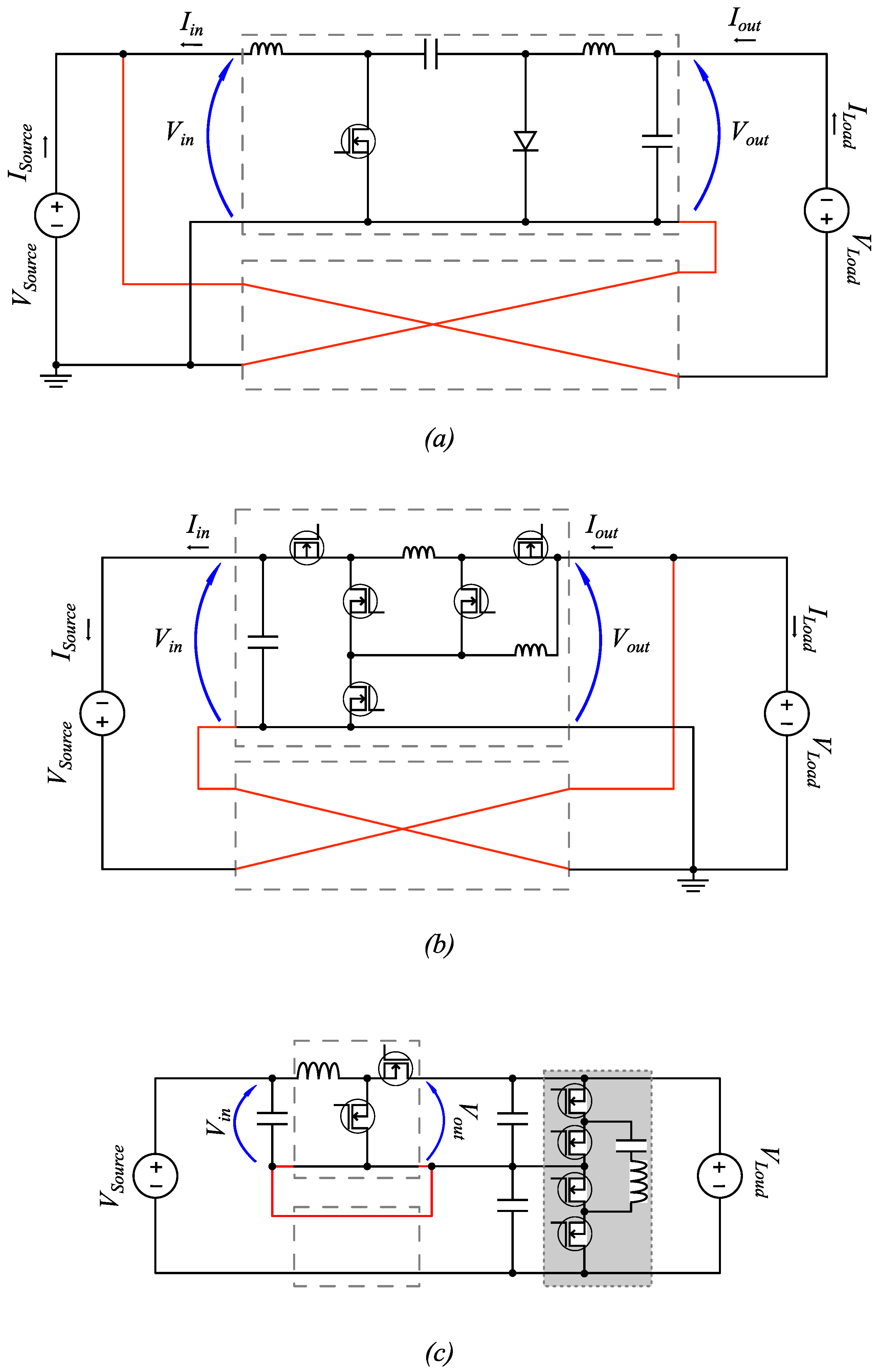
The DAB converter in Figure 6a has its input connected to , while its output is connected in series to , and both are connected to to give a straightforward example of the IPOS (a) case.
The outstanding feature of Figure 6b is that the authors reversed the . Carrying out KVL around the circuit yields , while if the load was wired as designated, it would yield IPOS (b).
Figure 6c demonstrates another attribute, which is the reversed . The right-hand side of the converter was flipped so that the negative of the converter’s output is connected to the positive side of the load, thus fulfilling the IPOS (c) topology.
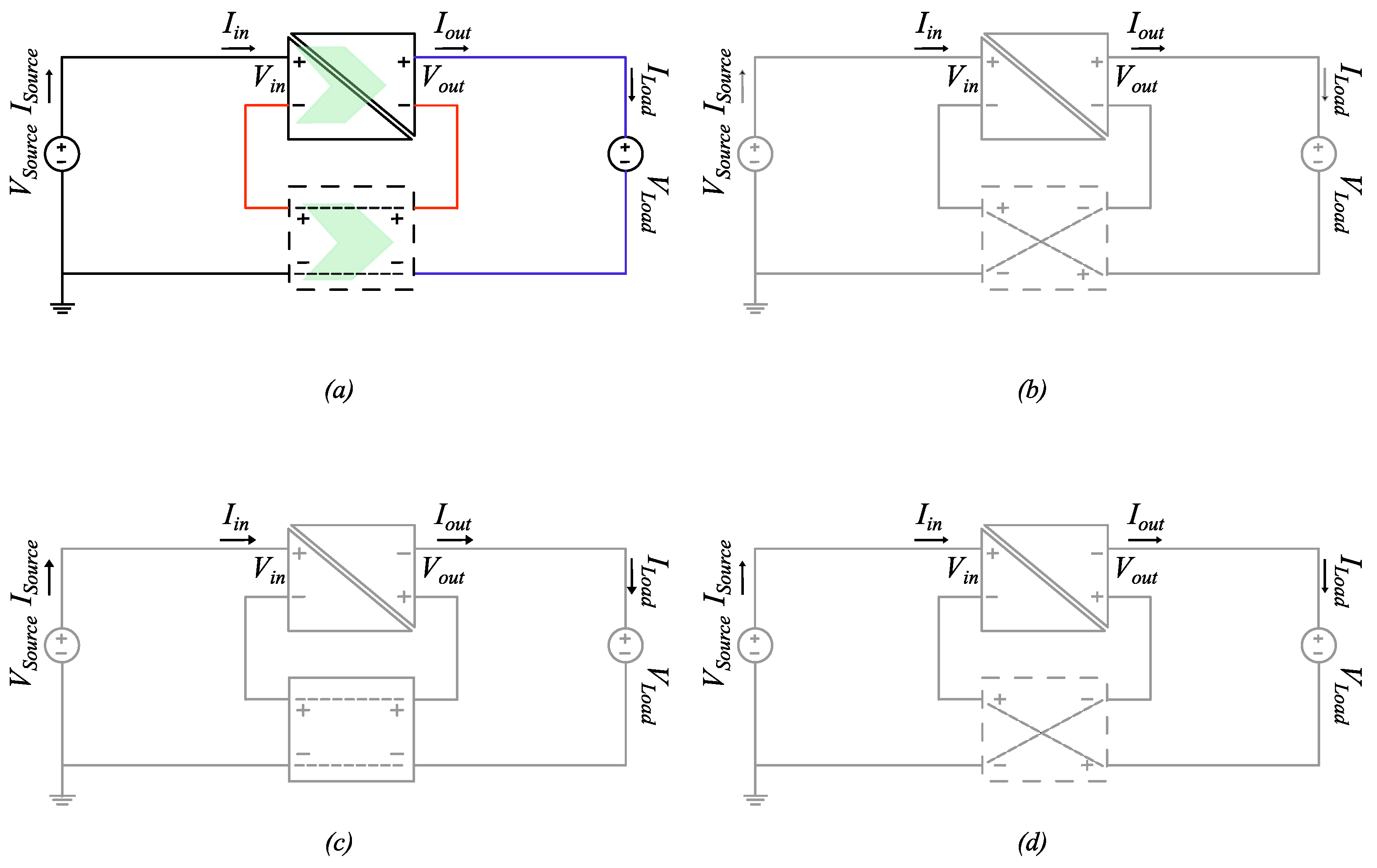
3.3. Input-Series-Output-Parallel Topology (ISOP)
Applying the same systematic approach of the previous Section 3.1 to the ISOP topology demonstrated in Figure 3b, four connections can be derived, as demonstrated in Figure 7.
Table 3 contains a summary of the equations describing the behavior of each topology. By utilizing the definition of and , Equations (19)–(21) are developed relevant to the topologies in Figure 7a,b,c, respectively.
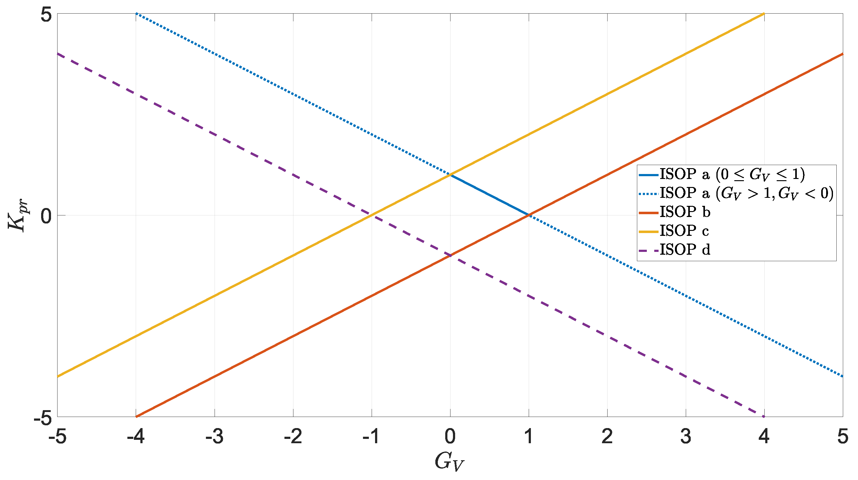
By plotting the Equations (19)–(22), Figure 8 can visualize the behavior of each ISOP topology. Starting with the ISOP (a) curve, it is seen that is bounded between 1 and 0, since will always be bigger than , so is not realizable. The ISOP (b) and (c) topologies can operate throughout the whole range of (including negative source voltage) with linear characteristics. ISOP (d) is also plotted in Figure 8 for review integrity, but it will not be practically achievable. One of the advantages of ISOP topology is that it reduces stress on semiconductor switches in high voltage applications [36].
3.4. ISOP-Based Converters
The work of Tao, Wang, and Zhuo [13] demonstrated using a converter to achieve four-quadrant operation. Their work is based on ISOP (a), providing bi-directional power flow between a DC bus and a battery of either a higher or lower voltage.
Renaudineau et al. [37] implemented ISOP (b) to generate rectified sinusoidal DC from a PV string input. In their simulation, they mitigated the harmonics content by relieving the inverter from high-frequency switching and dedicating it to unfolding only.
In [38], Anzola, Aizpuru, and Arruti proposed ISOP (a) for EV fast charging applications. Their simulation shows a steep drop of and as the State of Charge (SOC) builds up. A down-scaled prototype pf the PPP demonstrates a reduction of 65% in the size of the magnetic components, i.e., the transformer and inductor, when compared to the full power converter.
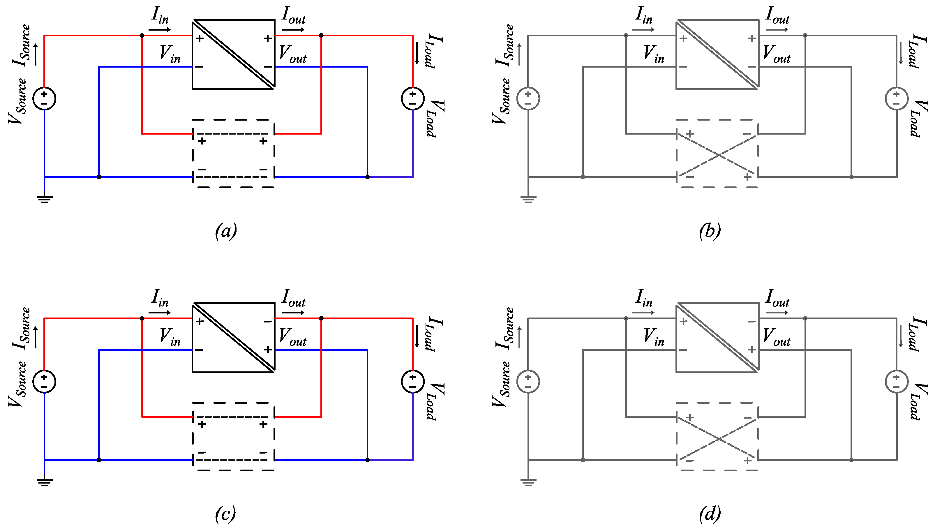
Table 4 displays a comparison between the reviewed ISOP systems, while Figure 9 presents examples of ISOP topologies.
Figure 9a represents a DAB-based ISOP (a) topology, where is connected in parallel to of the converter, while the same (i.e., ) is connected in series to , and then the sum of both voltages is connected to .
ISOP (b) topology is demonstrated in Figure 9b, where the flayback converter’s output is connected in parallel to , while its input voltage is connected in series between its output voltage and the source.
The full-bridge converter displayed in Figure 9c displays an inverted left-hand side, where the negative side of is connected to the positive side of .
3.5. Input-Series-Output-Series Topology (ISOS)
One more configuration can be deduced in the isolated topology group, which is Input-Series-Output-Series (ISOS). Figure 10 displays all the four combinations. By examining Figure 10a, the series connection (marked in red) can be seen on both sides of the input and the output.
By developing the power balance of the converter (for an ideal converter) in (23) with the aid of the current equations in Table 5, it can be seen that topologies (b) and (c) in Figure 10 are not achievable.
However, since , has a reversed direction in comparison to the designated direction in Figure 10b. This negative current reflected in (24) leads to a net positive power pouring into the converter, turning the converter into one that sinks power instead of transferring it.
A similar case can be deduced in the topology of ISOS (c); however, this time has a reversed sign but still leads to the same conclusion of the converter ending up sinking power. These observations halt any further study of those two arrangements.
On the other hand, in Figure 10d, the current will flow out of the positive terminals of the Load and Source as well, which is not a valid power transfer mode.
An attempt to flip the Load terminals in Figure 10d will end up yielding an identical topology to Figure 10a.
Maintaining the analysis method used in Section 3.1 and Section 3.3, the ISOS equations can be derived and summarized in Table 5.
Deriving in terms of produces an extra term in Equation (25). This term is represented by the ratio of to , and its effect will further be commented on in the upcoming Section 3.6.
By plotting Equation (25) for several values of as in Figure 11, the generic trends and the influence of ratio can be seen.
The trends in Figure 11 imply the necessity to hold at a steady value to maintain proper and predictable operation of the system.
3.6. ISOS-Based Converters
Within the surveyed and reviewed literature, the ISOS topology was the least encountered. The work seen in [41] contains an intermediate ISOS, utilized as a Half DC Bus Boost Converter, but no further details about its performance characteristics were developed. Ref. [42] described two converters connected in ISOS formation, with one of them having a 1:1 ratio, which can be thought of as the dummy converter stated earlier; however, it is introduced to achieve full galvanic isolation.
The work of Lopusina and Grbovic [43] illustrates explicitly an ISOS-topology converter; nevertheless, it is based on a non-isolated converter and hence will be seen in the upcoming Section 4.2.
3.7. Input-Parallel-Output-Parallel Topology (IPOP)
This arrangement represents a special case, since two out of its four variants will lead to short-circuiting the source with the load, leaving these scenarios out of the analysis. In the other two cases, will always be connected in parallel to , which leads to unity as expressed in (26).
Furthermore, can be seen in Figure 12, where cases (b) and (d) are also greyed out due to short-ciruits.
Although cases (a) and (c) in Figure 12 theoretically exist, their practical applications might not be of much interest due to the fact that is held steady to . Such fundamental restrictions limited the interest in further research on this type of topology, and therefore no related literature was found.
4. Non-Isolated PPP Architectures
Revisiting the topologies developed in the previous parts (Section 3.1 and Section 3.3), it can be seen that some topologies actually will not suffer from the short-circuit mentioned at the beginning of Section 3 when using non-isolated converters. Ref. [21] analytically developed all possible combinations for such arrangements, and based on that work, further analysis of operation is carried out in the following subsection. For simplicity purposes, this work will assume the use of a DC-DC boost converter, such as the one shown in Figure 13. Nevertheless, the analysis remains the same for any other type of non-isolated converter being used.
4.1. Fractional Topology
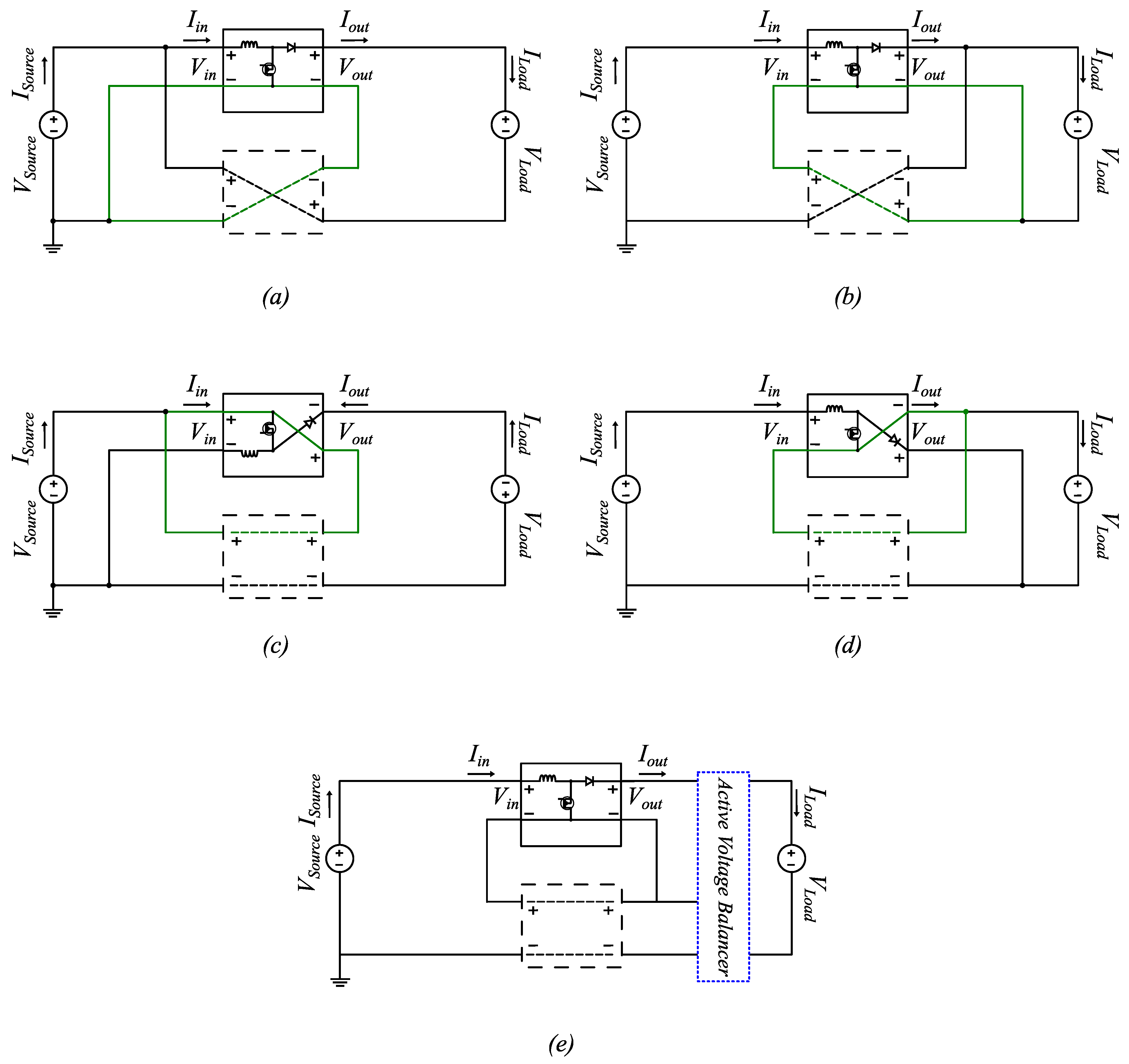
Looking back into the IPOS topologies demonstrated in Figure 4, it can be seen that for configuration IPOS (b), the negative terminal on each of the ports of the converter is actually connected to the same node. The same observation can also be seen in configuration ISOP (b) in Figure 7, as was already demonstrated for ISOS in Section 3.6. Such a remark means that a non-isolated converter can be connected directly in those topologies, where Figure 14 demonstrates the possible combinations of such non-isolated PPP topologies.
On the other hand, ref. [28] suggested solving the short-circuit problem by simply inverting the converter terminals. Figure 14c,d illustrate inverted boost converter connections. Such topologies are referred to in the literature as the Fractional Power Converter (FPC) [6]. It is to be noted that such configurations might lead to loss of partial power processing, as seen in [28]. The Active Voltage Balancer seen in Figure 14e is just one proposed arrangement, as seen in [44]; other arrangements might be proposed.
4.2. Fractional Topology-Based Converters
Due to the recent interest in the applications of non-isolated PPP, only a few examples could be found in the reviewed literature where an explicit non-isolated converter is used [4,29]. Kim and Parkhideh [45] presented a comparison between non-isolated and isolated converters for PVs and battery applications, where they stated higher efficiency for isolated PPC. The work presented in [6], based on the proposed Modified Inductor Boost Converter in [46], states that a of less than is achieved for a power conversion system of 750 W. The proposed topology in this work follows case (c) in Figure 14.
Another example can be found in the analytical and simulation work of the Cuk-based PPP converter in [47] connected according to case (a) in Figure 14. The authors suggested several Cuk-based converter topologies. However, no values were given about operating or .
In [48], the authors studied several scenarios of boost, buck, and buck–boost converters in the ISOS formation. A buck–boost prototype was implemented in the configuration of case (d) to develop a battery charger of kW.
The arrangement presented by [43] and demonstrated in Figure 15c has several salient points to be commented on. Firstly, it treats the voltage ratio mentioned earlier in Section 3.5 by using an Active Voltage Balancer that transfers bipolar DC into unipolar [44], and it is used to stabilize the Load voltage. The selected topology for the Active Voltage Balancer is a Series Resonant Balancer Converter (SRBC).
Second of all, due to the introduction of the Active Voltage Balancer in the design, a straightforward comparison is no longer valid with other topologies as the extra losses and the component count of the balancer have to be accounted for.
5. Conclusions
This review focuses on partial power processing technology, providing a comprehensive review from three aspects: structural classification, theoretical operation limits, and prototype examples. It discusses the principles of partial power processing technology, summarizes and clarifies the classification and naming of partial power structures in existing research, revisits the component stress factors and non-active power factor, and provides certain guidance for researching partial power DC converters.
Compared with traditional full-power solutions, partial power DC converters can achieve direct transmission of main power, with only a small portion of the system’s power being processed internally with a DC-DC converter, resulting in performance improvements in cost, volume, power density, efficiency, and thermal design. However due to the specific nature of its circuit structure, there are certain limitations in its application scenarios, and the applicability of partial power solutions needs to be considered in combination with specific scenario characteristics.
Existing research has essentially validated the energy efficiency advantages of PPC compared to traditional full-power converters. This work intends to contribute on the entry and foundation levels to the field of partial power conversion and act as a reference and base for further future development. In the future, further research can be conducted from the following two perspectives: In terms of research content, fault tolerance and fault detection techniques can be of interest as can exploring configurations based on resonant converters. Research and optimization for partial power solutions can be performed in multi-domain environments, such as vehicle-to-grid applications, green hydrogen production, kinetic energy recovery and regeneration for electric mobility, power supply for new data centers, hybrid energy storage systems, energy routers, etc.
Author Contributions
Conceptualization, R.G. and O.G.; methodology, R.G.; analysis, R.G. and R.R.; investigation, O.G.; writing—original draft preparation, O.G. and R.R.; writing—review and editing, R.G., O.G. and A.B.; visualization, O.G.; supervision, R.G. and A.B. All authors have read and agreed to the published version of the manuscript.
Funding
This work was supported by grant MCINN-22-TED2021-129796B-C21 and MCINN-23-PID2022-139479OB-C22 funded by MCIN/AEI/10.13039/501100011033. This work has been partially funded from the EUH2020 R&I Program under grant agreement 864459 (Project “TALENT”) and through ERFD Structural Funds. This work has been partially supported by PID2019-111051RB-100 (Project “B2B- Energy”).
Data Availability Statement
Not applicable.
Conflicts of Interest
The authors declare no conflict of interest.
References
- Li, C.; Cobos, J.A. Classification of Differential Power Processing Architectures Based on VA Area Modeling. IEEE J. Emerg. Sel. Top. Power Electron. 2022, 10, 7849–7866. [Google Scholar] [CrossRef]
- dos Santos, N.G.F.; Zientarski, J.R.R.; da Silva Martins, M.L. A Review of Series-Connected Partial Power Converters for DC–DC Applications. IEEE J. Emerg. Sel. Top. Power Electron. 2022, 10, 7825–7838. [Google Scholar] [CrossRef]
- Wouters, H.; Martinez, W. Bidirectional Onboard Chargers for Electric Vehicles: State-of-the-Art and Future Trends. IEEE Trans. Power Electron. 2024, 39, 693–716. [Google Scholar] [CrossRef]
- Anzola, J.; Aizpuru, I.; Romero, A.A.; Loiti, A.A.; Lopez-Erauskin, R.; Artal-Sevil, J.S.; Bernal, C. Review of Architectures Based on Partial Power Processing for DC-DC Applications. IEEE Access 2020, 8, 103405–103418. [Google Scholar] [CrossRef]
- Müller, S.; Deicke, M.; Doncker, R.W.D. Doubly fed induction generator systems for wind turbines. IEEE Ind. Appl. Mag. 2002, 8, 26–33. [Google Scholar] [CrossRef]
- Anzola, J.; Aizpuru, I.; Arruti, A.; Artal-Sevil, J.S.; Bernal, C. Demystifying Non-Isolated DC–DC Topologies on Partial Power Processing Architectures. Electronics 2022, 11, 480. [Google Scholar] [CrossRef]
- Liu, C.; Zhuang, K.; Pei, Z.; Zhu, D.; Li, X.; Yu, Q.; Xin, H. Hybrid SiC-Si DC–AC Topology: SHEPWM Si-IGBT Master Unit Handling High Power Integrated With Partial-Power SiC-MOSFET Slave Unit Improving Performance. IEEE Trans. Power Electron. 2022, 37, 3085–3098. [Google Scholar] [CrossRef]
- Kim, J.W. LLC Converter with Hold-Up Time Compensation using Partial Power Process with Semi-Active Bridge Rectifier. IEEE Trans. Power Electron. 2024; Early Access. [Google Scholar] [CrossRef]
- Lopez, D.; Muller, N.; Renaudineau, H.; Kouro, S.; Rodriguez, J. Partial power differential-mode inverter for photovoltaic microinverter applications. In Proceedings of the IECON 2021—47th Annual Conference of the IEEE Industrial Electronics Society, Toronto, ON, Canada, 13–16 October 2021. [Google Scholar] [CrossRef]
- de Andrade, J.M.; Coelho, R.F.; Lazzarin, T.B. Partial Power Processing and Efficiency Analysis of dc-dc Differential Converters. Energies 2022, 15, 1159. [Google Scholar] [CrossRef]
- Zapata, J.; Kouro, S.; Carrasco, G.; Renaudineau, H. Step-Up Partial Power DC-DC Converters for Two-Stage PV Systems with Interleaved Current Performance. Energies 2018, 11, 357. [Google Scholar] [CrossRef]
- Mira, M.C.; Zhang, Z.; Jorgensen, K.L.; Andersen, M.A.E. Fractional Charging Converter With High Efficiency and Low Cost for Electrochemical Energy Storage Devices. IEEE Trans. Ind. Appl. 2019, 55, 7461–7470. [Google Scholar] [CrossRef]
- Tao, X.; Wang, F.; Zhuo, F. A Four-quadrant Buck-boost Partial Power DC/DC Converter for Battery Energy Storage System. In Proceedings of the 2023 25th European Conference on Power Electronics and Applications (EPE’23 ECCE Europe), Aalborg, Denmark, 4–8 September 2023. [Google Scholar] [CrossRef]
- Abdel-Rahim, O.; Chub, A.; Blinov, A.; Vinnikov, D. Current-Fed Dual Inductor Push-Pull Partial Power Converter. In Proceedings of the 2022 IEEE 20th International Power Electronics and Motion Control Conference (PEMC), Brasov, Romania, 25–28 September 2022. [Google Scholar] [CrossRef]
- Liu, C.; Zhang, Z.; Ouyang, Z.; Andersen, M.A.E.; Zsurzsan, T.G. Analysis and Comparison of Isolated Converter based Step-Down Partial Power Processing Configurations. In Proceedings of the 2022 International Power Electronics Conference (IPEC-Himeji 2022-ECCE Asia), Himeji, Japan, 15–19 May 2022. [Google Scholar] [CrossRef]
- Zapata, J.W.; Kouro, S.; Carrasco, G.; Renaudineau, H.; Meynard, T.A. Analysis of Partial Power DC–DC Converters for Two-Stage Photovoltaic Systems. IEEE J. Emerg. Sel. Top. Power Electron. 2019, 7, 591–603. [Google Scholar] [CrossRef]
- Rojas, J.; Renaudineau, H.; Kouro, S.; Rivera, S. Partial power DC-DC converter for electric vehicle fast charging stations. In Proceedings of the IECON 2017—43rd Annual Conference of the IEEE Industrial Electronics Society, Beijing, China, 29 October–1 November 2017. [Google Scholar] [CrossRef]
- Wittenbreder, E. Topology selection by the numbers—Part one. Power Electron. Technol. 2006, 32, 32–36. [Google Scholar]
- Wittenbreder, E. Topology selection by the numbers—Part two. Power Electron. Technol. 2006, 33, 28–32. [Google Scholar]
- Hassanpour, N.; Chub, A.; Blinov, A.; Vinnikov, D. Comparison of Full Power and Partial Power Buck-Boost DC-DC Converters for Residential Battery Energy Storage Applications. In Proceedings of the 2022 IEEE 16th International Conference on Compatibility, Power Electronics, and Power Engineering (CPE-POWERENG), Birmingham, UK, 29 June–1 July 2022. [Google Scholar] [CrossRef]
- Jørgensen, K. Towards Partial Power Processing with Built in Impedance Spectroscopy. Ph.D. Thesis, Technical University of Denmark, Kgs. Lyngby, Denmark, 2020. [Google Scholar]
- Mira, M.C.; Zhang, Z.; Michael Andersen, A.E. Analysis and Comparison of dc/dc Topologies in Partial Power Processing Configuration for Energy Storage Systems. In Proceedings of the 2018 International Power Electronics Conference (IPEC-Niigata 2018-ECCE Asia), Niigata, Japan, 20–24 May 2018; pp. 1351–1357. [Google Scholar] [CrossRef]
- Liu, C. Partial Power Processing for High Efficient Power Converters. Ph.D. Thesis, Technical University of Denmark, Kgs. Lyngby, Denmark, 2023. [Google Scholar]
- Pittini, R.; Mira, M.C.; Zhang, Z.; Knott, A.; Andersen, M.A. Analysis and comparison based on component stress factor of dual active bridge and isolated full bridge boost converters for bidirectional fuel cells systems. In Proceedings of the 2014 International Power Electronics and Application Conference and Exposition, Shanghai, China, 5–8 November 2014; pp. 1026–1031. [Google Scholar] [CrossRef]
- Zientarski, J.R.R.; Martins, M.L.d.S.; Pinheiro, J.R.; Hey, H.L. Series-Connected Partial-Power Converters Applied to PV Systems: A Design Approach Based on Step-Up/Down Voltage Regulation Range. IEEE Trans. Power Electron. 2018, 33, 7622–7633. [Google Scholar] [CrossRef]
- IEEE Std 1459-2010; IEEE Standard Definitions for the Measurement of Electric Power Quantities Under Sinusoidal, Nonsinusoidal, Balanced, or Unbalanced Conditions. IEEE Power & Energy Society: Piscataway, NJ, USA, 2010. [CrossRef]
- Santos, N.G.F.; Hey, H.L.; Zientarski, J.R.R.; Martins, M.L.d.S. Piecewise Fryze power theory analysis applied to PWM DC–DC converters. IET Power Electron. 2020, 13, 2029–2038. [Google Scholar] [CrossRef]
- Zhao, J.; Yeates, K.; Han, Y. Analysis of high efficiency DC/DC converter processing partial input/output power. In Proceedings of the 2013 IEEE 14th Workshop on Control and Modeling for Power Electronics (COMPEL), Salt Lake City, UT, USA, 23–26 June 2013. [Google Scholar] [CrossRef]
- Anzola, J.; Aizpuru, I.; Arruti, A. Non-Isolated Partial Power Converter for Electric Vehicle Fast Charging Stations. In Proceedings of the 2020 IEEE 11th International Symposium on Power Electronics for Distributed Generation Systems (PEDG), Dubrovnik, Croatia, 28 September–1 October 2020. [Google Scholar] [CrossRef]
- Zapata, J.; Kouro, S.; Carrasco, G.; Meynard, T. Step-Down Partial Power DC-DC Converters for Two-Stage Photovoltaic String Inverters. Electronics 2019, 8, 87. [Google Scholar] [CrossRef]
- Mishra, S.; Tamballa, S.; Pallantala, M.; Raju, S.; Mohan, N. Cascaded Dual-Active Bridge Cell Based Partial Power Converter for Battery Emulation. In Proceedings of the 2019 20th Workshop on Control and Modeling for Power Electronics (COMPEL), Toronto, ON, Canada, 17–20 June 2019. [Google Scholar] [CrossRef]
- Zheng, K.; Zhang, W.; Wu, X.; Jing, L.; Zhao, H. Partial Power Conversion for Increased Energy Storage Capability of Li-ion Battery Energy Storage System. IEEE Trans. Ind. Electron. 2023, 71, 4742–4752. [Google Scholar] [CrossRef]
- Abdel-Rahim, O.; Chub, A.; Blinov, A.; Vinnikov, D. Performance Evaluation of Step-Up/Down Current-Source Partial Power Converters for PV Applications. In Proceedings of the 2022 IEEE 63th International Scientific Conference on Power and Electrical Engineering of Riga Technical University (RTUCON), Riga, Latvia, 10–12 October 2022; pp. 1–5. [Google Scholar] [CrossRef]
- Köse, H.; Aydemir, M.T. Design and implementation of a 22kW full-bridge push–pull series partial power converter for stationary battery energy storage system with battery charger. Meas. Control 2020, 53, 1454–1464. [Google Scholar] [CrossRef]
- Min, B.D.; Lee, J.P.; Kim, J.H.; Kim, T.J.; Yoo, D.W.; Song, E.H. A New Topology With High Efficiency Throughout All Load Range for Photovoltaic PCS. IEEE Trans. Ind. Electron. 2009, 56, 4427–4435. [Google Scholar] [CrossRef]
- Wei, R.; Ding, L.; Li, Y. Efficiency-Oriented Optimized Design and Control of Hybrid FSBB-CLLC Converters with Partial Power Processing Capability. IEEE Trans. Power Electron. 2024; Early Access. [Google Scholar] [CrossRef]
- Renaudineau, H.; Flores-Bahamonde, F.; Kouro, S.; Zapata, J.W. Single-Phase partial power unfolding inverter for photovoltaic string application. In Proceedings of the 2021 IEEE 30th International Symposium on Industrial Electronics (ISIE), Kyoto, Japan, 20–23 June 2021. [Google Scholar] [CrossRef]
- Anzola, J.; Aizpuru, I.; Arruti, A. Partial Power Processing Based Converter for Electric Vehicle Fast Charging Stations. Electronics 2021, 10, 260. [Google Scholar] [CrossRef]
- Gao, S.; Zhang, Y.; Wang, Y.; Liu, J.; Xu, D. An Optimal Control Strategy for the DAB-Based Partial Power Converter Based on Extended-Phase-Shift Control. IEEE Open J. Power Electron. 2023, 4, 817–827. [Google Scholar] [CrossRef]
- Hernandez, M.S.; Renaudineau, H.; Concha, D.; Llor, A.M. Series Partial Power Pre-Regulator for DCX-based Stand-Alone Green Hydrogen Production. In Proceedings of the 2021 IEEE 30th International Symposium on Industrial Electronics (ISIE), Kyoto, Japan, 20–23 June 2021. [Google Scholar] [CrossRef]
- Grbović, P.J.; Delarue, P.; Le Moigne, P. Boost diode rectifier for three-phase variable speed drives supplied from the single-phase mains: Analysis and design. In Proceedings of the IECON 2012—38th Annual Conference on IEEE Industrial Electronics Society, Montreal, QC, Canada, 25–28 October 2012; pp. 274–280. [Google Scholar] [CrossRef]
- Giri, R.; Ayyanar, R.; Ledezma, E. Input-series and output-series connected modular DC-DC converters with active input voltage and output voltage sharing. In Proceedings of the Nineteenth Annual IEEE Applied Power Electronics Conference and Exposition, 2004, APEC’04, Anaheim, CA, USA, 22–26 February 2004; Volume 3, pp. 1751–1756. [Google Scholar] [CrossRef]
- Lopušina, I.; Grbović, P. Comparative Analysis of Input-Series-Output-Series Partial Power Rated DC to DC Converters. In Proceedings of the 2021 21st International Symposium on Power Electronics (Ee), Novi Sad, Serbia, 27–30 October 2021; pp. 1–7. [Google Scholar] [CrossRef]
- Wang, F.; Lei, Z.; Xu, X.; Shu, X. Topology Deduction and Analysis of Voltage Balancers for DC Microgrid. IEEE J. Emerg. Sel. Top. Power Electron. 2017, 5, 672–680. [Google Scholar] [CrossRef]
- Kim, N.; Parkhideh, B. Comparative Analysis of Non-Isolated and Isolated Type Partial-Power Optimizers for PV-Battery Series Inverter Architecture. In Proceedings of the 2018 IEEE Energy Conversion Congress and Exposition (ECCE), Portland, OR, USA, 23–27 September 2018. [Google Scholar] [CrossRef]
- Sadaf, S.; Bhaskar, M.S.; Meraj, M.; Iqbal, A.; Al-Emadi, N. A Novel Modified Switched Inductor Boost Converter With Reduced Switch Voltage Stress. IEEE Trans. Ind. Electron. 2021, 68, 1275–1289. [Google Scholar] [CrossRef]
- Artal-Sevil, J.; Anzola, J.; Ballestín-Bernad, V.; Bernal-Agustín, J. Analysis and Implementation of different non-isolated Partial-Power Processing Architectures based on the Cuk Converter. In Proceedings of the 2022 24th European Conference on Power Electronics and Applications (EPE’22 ECCE Europe), Hannover, Germany, 5–9 September 2022; pp. 1–10. [Google Scholar]
- Xue, F.; Yu, R.; Huang, A. Fractional converter for high efficiency high power battery energy storage system. In Proceedings of the 2017 IEEE Energy Conversion Congress and Exposition (ECCE), Cincinnati, OH, USA, 1–5 October 2017; pp. 5144–5150. [Google Scholar] [CrossRef]
Figure 1.
PPP family tree influenced by [4], with the scope of the current work highlighted.
Figure 1.
PPP family tree influenced by [4], with the scope of the current work highlighted.

Figure 2.
Fryze power factor for different topologies of isolated PPC operating at different .

Figure 3.
PPC configurations: (a) Isolated converter’s output connected in series with the dummy converter’s output to produce IPOS topology. (b) Series connection between the input of the isolated converter and the input of the dummy converter to produce ISOP topology. (c) Series connections for both sides of the isolated and dummy converters giving rise to ISOS topology. (d) IPOP diagram showing source connected in parallel to the load, which will be analyzed further in Section 3.7.

Figure 4.
IPOS configurations: (a–c) are three realizable variants of IPOS topology, and (d) is the fourth analytical case, not achievable in reality. The arrow inside the dummy converter indicates the direct power flow, while the arrow inside the isolated converter indicates the power flow within the converter itself. Note the sign change of the converters.

Figure 5.
IPOS : IPOS (a) based on (15), with the part of shaded out. IPOS (b) from (16). IPOS (c) from (17) with shaded out. IPOS (d) was plotted to maintain the review integrity.

Figure 6.
Examples of IPOS topologies in the literature: (a) IPOS-a topology implemented in [31]. (b) IPOS-b seen in work of Liu et al. [15], with reversed . (c) IPOS-c topology from [33]; notice the reversed arrow to indicate flipped output.

Figure 7.
ISOP configurations: (a–c) are three realizable variants of ISOP topology, and (d) is the fourth analytical case, not achievable in reality. The arrow inside the dummy converter indicates the direct power flow, while the arrow inside the isolated converter indicates the power flow within the converter itself. Note the sign change of the converters.

Figure 8.
ISOP : ISOP (a) topology trend from (19) with shaded out. ISOP (b) trend (20) and shaded out. ISOP (c) trend from (21). ISOP (d) was plotted in this figure as another graphical proof that will be negative over the whole range of operation, hence rendering this mode invalid.

Figure 9.
Examples of ISOP in the reviewed literature: (a) DAB-based ISOP (a) from [39]. (b) ISOP (b) flyback. (c) ISOP (c) integrated full bridge [37]; note the inverted .

Figure 10.
ISOS configurations: (a,d) are two realizable variants of ISOS topology, while (b,c) are analytical cases not achievable in reality. The arrow inside the dummy converter indicates the direct power flow, while the arrow inside the isolated converter indicates the power flow within the converter itself. Note the sign change of the converters.

Figure 11.
ISOS : Linear relation between and at different ratios.

Figure 12.
IPOP combinations: (a,c) might share load current. (b,d) will cause short-circuits.

Figure 13.
(a) Boost converter. (b) Block representation.

Figure 14.
Realizable variants of non-isolated PPP topologies: (a) IPOS-b non-inverted. (b) ISOP-b non-inverted. (c) IPOS-c inverted. (d) ISOP-c non-inverted. (e) ISOS non-inverted. The green path represents a redundant loop.
Figure 14.
Realizable variants of non-isolated PPP topologies: (a) IPOS-b non-inverted. (b) ISOP-b non-inverted. (c) IPOS-c inverted. (d) ISOP-c non-inverted. (e) ISOS non-inverted. The green path represents a redundant loop.

Figure 15.
Examples of non-isolated PPC: (a) Cuk converter FPC demostrated in [47]. (b) Modified Inductor FPC topology seen in [6,46]. (c) Boost FPC studied by [43]; shaded area represents Active Voltage Balancer.

Table 1.
Summery of IPOS equations.
| Source | Load | Connection Diagram from Figure 4 |
|---|---|---|
| (a) | ||
| (b) | ||
| (c) | ||
| (a) | ||
| (b) | ||
| (c) |
Table 3.
Summery of ISOP equations.
| Source | Load | Connection Diagram from Figure 7 |
|---|---|---|
| (a) | ||
| (b) | ||
| (c) | ||
| (a) | ||
| (b) | ||
| (c) |
Table 4.
Reviewed ISOP-based PPC.
| Reference | Converter | Topology | Application | System Power [kW] | [%] | ||
|---|---|---|---|---|---|---|---|
| [13] | H-bridge+CLLC | ISOP (a) | 16% | 1.00 | Battery | 45.0 | 97.91 |
| [39] | DAB | ISOP (a) | 25% | 0.75 | EV | 1.00 | 97.00 |
| [16] | isolated full-bridge | ISOP (a) | 13% | 0.84 | PV | 0.82 | 98.50 |
| [16] | Full-bridge | ISOP (b) | 11% | 1.10 | PV | 1.00 | 97.50 |
| [38] | DAB | ISOP (a) | 19% | 0.45 | Battery | 2.20 | 99.62 |
| [40] | Integrated full-bridge | ISOP (a) | 25% | 0.75 | PV | 2.0 | 98.60 |
| [37] | Full-bridge | ISOP (a) | 12% | 0.89 | PV | 3.30 | 97.50 |
| [28] | Flyback | ISOP (c) | 58% | 1.40 | PV | 0.10 | 92.00 |
Table 5.
Summary of ISOS equations.
| Source | Load | Figure 10 Diagram | Viability |
|---|---|---|---|
| (a) | yes | ||
| (b) | no | ||
| (c) | no | ||
| (d) | no | ||
| (a) | yes | ||
| (b) | no | ||
| (c) | no | ||
| (d) | no |
Table 6.
Summery of non-isolated PPP equations.
| Source | Load | Connection Diagram from Figure 14 |
|---|---|---|
| (a) | ||
| (b) | ||
| (c) | ||
| (d) | ||
| (e) | ||
| (a) | ||
| (b) | ||
| (c) | ||
| (d) | ||
| (e) |
Disclaimer/Publisher’s Note: The statements, opinions and data contained in all publications are solely those of the individual author(s) and contributor(s) and not of MDPI and/or the editor(s). MDPI and/or the editor(s) disclaim responsibility for any injury to people or property resulting from any ideas, methods, instructions or products referred to in the content. |
© 2024 by the authors. Licensee MDPI, Basel, Switzerland. This article is an open access article distributed under the terms and conditions of the Creative Commons Attribution (CC BY) license (https://creativecommons.org/licenses/by/4.0/).
Share and Cite
MDPI and ACS Style
Gsous, O.; Rizk, R.; Barbón, A.; Georgious, R. Review of DC-DC Partial Power Converter Configurations and Topologies. Energies 2024, 17, 1496. https://doi.org/10.3390/en17061496
AMA Style
Gsous O, Rizk R, Barbón A, Georgious R. Review of DC-DC Partial Power Converter Configurations and Topologies. Energies. 2024; 17(6):1496. https://doi.org/10.3390/en17061496
Chicago/Turabian StyleGsous, Omar, Reem Rizk, Arsenio Barbón, and Ramy Georgious. 2024. "Review of DC-DC Partial Power Converter Configurations and Topologies" Energies 17, no. 6: 1496. https://doi.org/10.3390/en17061496
Note that from the first issue of 2016, this journal uses article numbers instead of page numbers. See further details here.