
The Effect of Deposition Time Optimization on the Photovoltaic Performance of Sb2Se3 Thin-Film Solar Cells
School of Electrical Engineering, Northeast Electric Power University, Jilin 132012, China
*
Author to whom correspondence should be addressed.
Energies 2024, 17(8), 1937; https://doi.org/10.3390/en17081937
Submission received: 27 February 2024
/
Revised: 5 April 2024
/
Accepted: 10 April 2024
/
Published: 18 April 2024
(This article belongs to the Topic Cooperative Localization, Optimization and Control of Networked Autonomous Systems: Theories, Analysis Tools and Applications)
Abstract
:Antimony selenide (Sb2Se3) photovoltaic thin-film materials have been recognized as suitable thin-film photovoltaic candidates for sustainable development due to the low toxicity of their constituent elements and abundant reserves. In this study, we employed the close space sublimation (CSS) method to fabricate solar cells with the FTO/SnO2/Sb2Se3/P3HT/C device architecture. By optimizing the deposition time, we achieved (hk1) orientation-preferred Sb2Se3 films, the optimized device exhibited a peak efficiency of 5.06%. This work investigated the growth mechanism of antimony selenide using a complete characterization technique, while the experimental parameters were simulated and matched using Widget Provided Analysis of Microelectronic and Photonic Structures (wxAMPS) showing excellent potential in the deposition of optoelectronic thin films by close space sublimation.
1. Introduction
As a key technology for electrical energy conversion, solar cells have great potential to replace non-renewable fossil fuels [1,2]. Thin-film solar cells have offered more possibilities for the promotion and utilization of renewable energy in areas such as photovoltaic buildings and intelligent robots due to their many advantages, such as high material utilization efficiency, low energy consumption, high power generation rate, and flexible scalability [3,4,5]. New types of group III and V materials, like Copper Zinc Tin Sulfide (CZTS), Cadmium Telluride (CdTe), and metal halide perovskites, have been applied in thin-film solar cells [6,7,8]. However, the inherent toxicity of cadmium, the scarcity of elements such as tellurium, indium, and gallium, and the sensitivity of metal halide chalcogenides and CZTS materials to oxidation, sulfation, and hydrolysis have severely limited the sustainable development of these thin-film solar cell technologies [9,10,11,12].
In recent years, the emerging photovoltaic thin-film material antimony selenide (Sb2Se3) has been considered a very promising candidate for future thin-film solar cells [13,14]. The toxicity of the constituent elements Sb and Se is extremely low, and they are abundant on earth, ensuring a sustainable supply of Sb and Se [15,16]. The bandgap of Sb2Se3 films ranges between 1.1 eV and 1.3 eV, characterized by high short-wavelength light absorption (>105 cm−1), high electron mobility (10 cm2V−1s−1), and low material toxicity [17]. As an emerging solar cell, various manufacturing techniques for Sb2Se3 films have been reported, such as close-spaced sublimation (CSS) [18], chemical molecular beam deposition (CMBD) [19], vapor transport deposition (VTD) [20], and electrodeposition [21]. Additionally, magnetron sputtering [22], chemical bath deposition (CBD) [23], and ultrasonic spray pyrolysis (USP) [24] techniques have been successfully employed in the fabrication processes of antimony selenide solar cells. The application of these technologies has not only facilitated improvements in the performance of antimony selenide solar cells but also provided new strategies for the commercialization of future solar cells.
Sb2Se3 has a unique quasi-one-dimensional crystal structure consisting mainly of (Sb4Se6)n ribbons. The carrier transport efficiency along the (Sb4Se6)n ribbons is much higher than that across the ribbons [25,26]. Therefore, to optimize Sb2Se3 solar cells, it was essential to select appropriate manufacturing techniques to precisely control the growth orientation of the Sb2Se3 thin films and ensure that their vertical conductivity was enhanced. Moreover, by engineering means to further optimize the crystal structure and orientation of Sb2Se3 materials, it was anticipated to further improve their application performance in photovoltaic and photoelectric fields. Lin et al. demonstrated that Sb2Se3 with (hk1) orientation proved more favorable for enhancing carrier collection compared to (hk0) orientation. Sb2Se3 films oriented along (211) and (221) exhibit lower resistivity as opposed to the (120) orientation [27]. Furthermore, Zhou et al. found that the (001)-oriented Sb2Se3 film could provide excellent carrier migration efficiency [28]. Capitalizing on the particular characteristic of Sb2Se3 crystals, Mai’s team employed the CBD method to fabricate high-quality Sb2Se3 nanorod arrays along the [001] direction, providing profound insights into the 1D structure and applications of Sb2Se3 crystals [29]. Therefore, meticulous control over the crystal orientation of Sb2Se3 thin films to attain a preferred (hk1) orientation is indispensable for optimizing their conversion efficiency in solar cells.
Sb2Se3 has a relatively high saturation vapor pressure in the range of 450 to 500 °C, which provides ideal conditions for the formation of stable compounds in the gas phase [30]. Wang et al. demonstrated the growth process of Sb2Se3 films and the formation mechanism of Sb2Se3 nanorods appearing on Sb2Se3 films by the VTD method [31]. Tao et al. demonstrated the potential of the CSS technique in investigating the microstructure of the Sb2Se3 photoactive layer by independently controlling the source and substrate temperatures, resulting in high-quality Sb2Se3 thin films with a (hk1)-preferred orientation [32]. Its sublimation properties allow it to transform directly from solid to gas at lower temperatures, which makes the CSS method a suitable technique to be utilized for controlling the deposition process of antimony selenide thin films. The CSS technique, as an advanced deposition approach equipped with real-time monitoring and control devices, enables precise optimization of deposition conditions, facilitating finer control over film quality and properties. Rijal et al. utilized a closed-space sublimation followed by a selenization approach to fabricate Sb2Se3 solar cells, investigating the influence of selenization temperature on the structural and morphological properties of Sb2Se3 films as well as the corresponding photovoltaic performance of the devices [33]. Fan et al. templated the growth of vertically oriented columnar Sb2Se3 absorber layers via closed-space sublimation, achieving high-quality Sb2Se3 absorber layers with passivation by controlling the crystal grain orientation and density of Sb2Se3 seeds [34].
Additionally, numerical simulation, a vital theoretical tool for probing photovoltaic device performance, facilitates precise modifications to device structure and film parameters. Cao et al. utilized wxAMPS simulation software to model and simulate three different electron transport layer configurations (CdS, ZnO, and SnO2) applied to Sb2Se3 solar cells, demonstrating that Sb2Se3 thin-film solar cells can achieve excellent optoelectronic performance with a simple device structure [35]. Memari et al. simulated colloidal CPQD solar cells with a 14.61% efficiency using minimal fitting parameters in SCAPS-1D and, through experimental and simulation analysis, comprehensively evaluated the photovoltaic performance of high-efficiency, flexible CPQD solar cells from a research standpoint [36]. Comparing simulation results with experimental data revealed the model’s shortcomings and biases, thus enhancing the accuracy and reliability of the simulations. Data fitting and analysis facilitated a deeper understanding of the performance and behavior of solar cells, inspiring strategies to improve energy conversion efficiency. This included evaluating the performance of solar cells under different lighting conditions and exploring ways to optimize performance through material and structural adjustments [37]. Additionally, data fitting was crucial for optimizing manufacturing techniques, not only deepening the understanding of thin-film solar cell technology but also revealing which parameters were most critical and how to adjust them for optimal performance.
In this study, high-quality Sb2Se3 films with (hk1)-preferred orientation were successfully deposited using the CSS technique and applied to the preparation of solar cell devices with FTO/SnO2/Sb2Se3/P3HT/C structure. The effects of deposition time on the crystal orientation, interfacial properties and device performance of Sb2Se3 solar cells were systematically investigated, and the formation mechanism of (hk1)-oriented Sb2Se3 films was discussed in detail. The results indicated that appropriate deposition times facilitated the achievement of uniform grain distribution, moderate grain size, and reduced defect density in Sb2Se3rdin films, which contributed to enhanced carrier transport efficiency and, consequently, improved photovoltaic performance of the devices. Furthermore, through simulation and emulation, the optimal device’s experimental data were successfully matched, validating the rationality of the experimental design and the accuracy of the experimental operations. Additionally, simulation allowed researchers to gain a deeper understanding of how these processes affected the overall performance of the devices, thereby providing theoretical guidance for optimizing device design and material selection. This study demonstrated the significant potential of CSS technology in depositing photovoltaic thin films with specific crystal orientations and served as a reference for integrating experimental and simulation analyses in the study of thin-film solar cells.
2. Materials and Methods
2.1. Materials
The FTO substrate (TEC15) was supplied by Youxuan New Energy Technology Co., Ltd. (Shenyang, China). The SnO2 colloid solution (tin (IV) oxide, 15% in H2O colloidal dispersion) and 1,2-Dichlorobenzene (o-DCB, 99%) were purchased from Alfa Aesar. Sb2Se3 powder (99.999%) was purchased from Ketai New Material Co., Ltd. (Nanchang, China). Polymer Light Technology Inc. (Xi’an, China) supplied the Regioregular poly (3-hexylthiophene) (P3HT). The low-temperature conductive carbon paste was supplied by MaterWin Co., Ltd. (Shanghai, China).
2.2. Device Fabrication
The composition of the Sb2Se3 solar cell under investigation is depicted in Figure 1a. The FTO substrate (2.5 × 2.5 cm) underwent sequential ultrasonic cleaning with deionized water, ethanol, and isopropanol in a glass cleaning rack, with each cleaning lasting 8 min. Subsequently, any residual alcohol solution was removed from the glass surface using nitrogen and dried in a homemade UV-Ozone cleaner for 30 min. This cleaning procedure ensures the FTO substrate is thoroughly cleaned, thereby guaranteeing accurate and reproducible experimental outcomes. Following this, the SnO2 electron transport layer was prepared using a SnO2 nanoparticle dispersion as a precursor solution. The pristine SnO2 colloidal solution was spin-coated onto the cleaned FTO substrate twice at 2000 r/min for 60 s. After the spin-coating process, the FTO substrate was transferred to a heated bench and annealed in an air atmosphere at 150 °C for 30 min to form a dense tin dioxide electron transport layer, resulting in the formation of a dense SnO2 electron transport layer. Tin dioxide was chosen as the electron transport layer due to its excellent electron transport properties and suitable electron mobility, thereby enhancing the charge transfer efficiency of antimony selenide solar cells. Furthermore, the high transmittance of tin dioxide enhances the light absorption of antimony selenide solar cells, maximizing the conversion of light energy into electrical energy.
By forming a dense SnO2 film on the FTO substrate, effective prevention of photogenerated carrier recombination was achieved, thereby maximizing the photoelectric conversion efficiency. In addition, we conducted transmittance tests on the FTO-SnO2, with Figure 1a displaying the transmittance for both the FTO substrate without spin-coated SnO2 and that with FTO-SnO2. After the fabrication of the SnO2 electron transport layer on the FTO substrate, the transmittance of the FTO-SnO2 films did not decrease; the transmittance at the FTO substrate at 400 nm was approximately 61%, while it increased to around 72% for the FTO-SnO2 films. This can be attributed to the lower surface roughness of FTO-SnO2, which resulted in reduced light scattering and increased direct transmittance. Furthermore, the transmittance of FTO-SnO2 remained stable at around 80% for wavelengths of approximately 500 nm and above, and its high transmittance in the visible range (400~550 nm) enables light to reach the light-absorbing layer more effectively.
Subsequently, Sb2Se3 powder was loaded into the chamber of a customized CSS device as the evaporation source, facilitating the vacuum evaporation of the Sb2Se3 film onto the SnO2 electron transport layer. A schematic representation of the preparation process is provided in Figure 1b. The deposition rate was controlled by resistive wire current, and Sb2Se3 films were deposited in a vacuum of 1 Pa with an evaporation distance of 10 mm. Conducting the sublimation process under vacuum prevents interference from gases or impurities, ensuring a stable environment for antimony selenide powder sublimation and preventing oxidation and other undesired reactions. The graphite substrate of the Sb2Se3 source was connected to the instrument panel with a sensor in our CSS device, and the temperature difference between the source and the target was strictly controlled and monitored. The temperature difference between the source temperature and the target temperature was tested to be within ±5 °C. Before deposition, the substrate was preheated for a period of time. Once the evaporation source temperature reaches 250 °C, the SnO2-coated FTO glass substrate is transferred from the loading chamber to the CSS unit. Subsequently, the temperature is held at 350 °C for 20 min to ensure uniform temperature distribution in the chamber for the antimony selenide powder. Deposition of the Sb2Se3 film then begins at 520 °C, with the shutter between the deposition source and the substrate closed to initiate the growth of Sb2Se3 grains on the substrate. Deposition times are set at 40, 50, 60, and 70 s, respectively. After completion of the process, the shield is opened, the heater is turned off, and the film is returned to the loading chamber to cool to room temperature before removal, achieved by purging the chamber with nitrogen gas to release the vacuum. During the cooling phase, special care was taken to ensure a gradual reduction in temperature to avoid thermal shock, which could potentially induce cracks or dislocations within the crystalline structure of the films. The cooling rate was meticulously controlled, with a steady decrease in temperature over a predefined time period, to allow for the proper annealing of the films. This annealing step is vital for relieving any internal stresses developed during the deposition process and for promoting the crystallinity of the Sb2Se3 films.
Moreover, a 20 mg/mL solution of P3HT was prepared by accurately weighing 20 mg of P3HT and dissolving it in 1 mL of 1,2-Dichlorobenzene. The solution was then stirred at 50 °C for 5 h using a magnetic stirrer to ensure complete dissolution. Subsequently, 80 μL drops of the P3HT solution were dispensed onto the sample film using a pipette gun and spin-coated at 2000 rpm for 60 s. Then, anneal in an air atmosphere at a temperature of 120 °C for 10 min to uniformly disperse the P3HT hole transport layer on the Sb2Se3 thin film. As an organic semiconductor material with good hole transport properties, P3HT can effectively transport photogenerated holes from the Sb2Se3 film to the electrode, which helps to improve the charge collection efficiency of the photovoltaic cell. In the processing of P3HT hole transport layers, the annealing temperature had a significant impact on promoting the rearrangement and interaction of molecular chains within the material, thereby affecting device performance. Higher annealing temperatures were found to improve the orderliness of P3HT chains, potentially increasing the photoelectric conversion efficiency of the films. However, excessively high annealing temperatures could also lead to structural damage in P3HT, impacting the overall performance of the films. Moreover, the P3HT hole transport layer can regulate the energy level difference between Sb2Se3 and the electrode, which helps to improve the photogenerated carrier transport efficiency and thus enhance the photoelectric conversion efficiency.
Finally, carbon electrodes were fabricated using carbon paste. This process involved placing a homemade mask plate on the surface of the film and then uniformly applying the carbon paste using a scraping method. Subsequently, the carbon electrodes were annealed in an air atmosphere at 150 °C for 30 min to promote curing. Carbon electrodes were chosen because they do not involve the use of rare materials or harmful chemicals in their preparation and are environmentally friendly in line with sustainable development. At the same time, carbon electrodes have high chemical stability at room temperature, which can withstand chemical reactions during battery operation and extend the service life of the battery. The structure of the final prepared Sb2Se3 thin-film solar cell device is shown in Figure 1c. The electrodes possessed a circular cross-section with an area of 0.07 cm2.
2.3. Characterization
The microstructure of Sb2Se3 thin films was characterized by scanning electron microscopy (SEM) (Sigma, Zeiss, Jena, Germany), and surface topography and cross-sectioning of material samples were carried out to realize the analysis of sample crystallization and densification. The X-ray diffraction (XRD) patterns of the Sb2Se3 films were analyzed using a diffractometer (XRD-7000, Shimadzu, Tokyo, Japan). CuKa radiation was employed as the radiation source, with an incident wavelength of 1.5406 Å and a voltage of 40 kV. The scanning range was set between 10°and 60°, and the samples were characterized at a scanning speed of 10° min−1. The solar simulator (SS100A, Photo Emission Tech Inc., Moorpark, CA, USA) was employed for the measurement of current density–voltage (J-V) characteristics. The solar simulator, class AAA, generated incident solar radiation with an intensity of 100 mW/cm2 using the AM 1.5 spectrum at a test temperature of 25 °C. Electrical performance parameters such as open-circuit voltage (Voc), short-circuit current censity (Jsc), fill factor (FF), photoelectric conversion efficiency (PCE) were obtained for solar cell installations under light. The external quantum efficiency (EQE) spectra were obtained using the quantum efficiency system (SCS100, Zolix Co., Ltd., Beijing, China) for the analysis of photovoltaic response efficiency and the loss of photocurrent in solar cells, indicating the ratio of the number of charge carriers to the number of incident photons introduced externally. The scanning range was set from 300 to 1100 nm, with a scanning speed of 5 nm/s.
3. Results
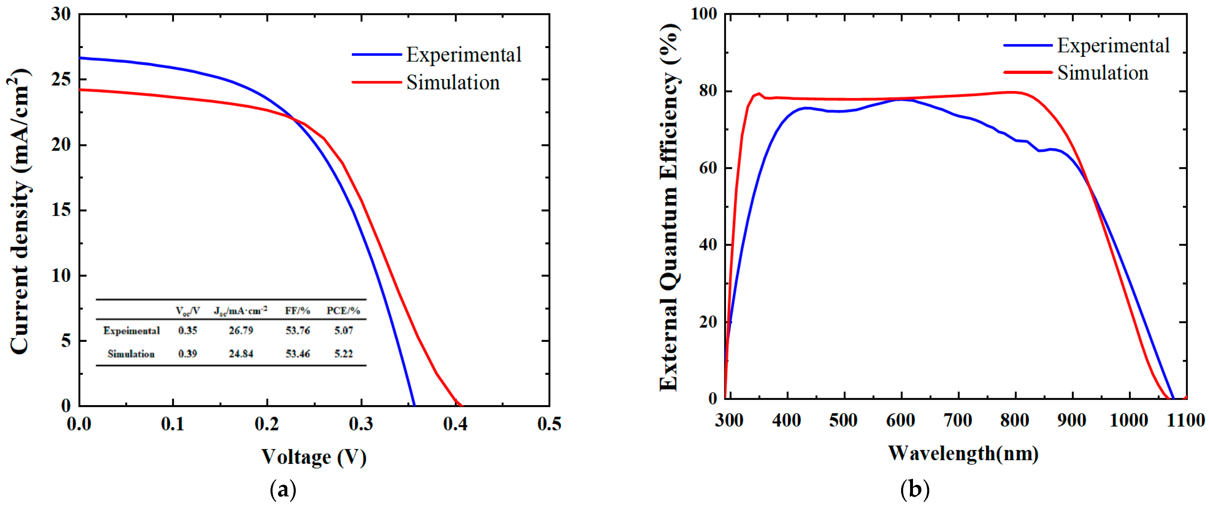
The EQE and J-V curves of the experimental results were simulated and analyzed using the wxAMPS software, as shown in Figure 2. During the simulation, we considered two key electrode materials as a function of FTO (tin fluoride oxide) and C (carbon), which are 4.4 and 5.0 eV, respectively. Accurately setting these figures of merit was crucial for simulating the optoelectronic device’s behavior. In the optical part of the simulation, we considered the incidence of sunlight from the FTO side and set the light reflectivity of the top and bottom electrodes to 0% and 100%, respectively. Surface recombination velocities for the front and back contacts are both 1 × 107 cm/s. This design fully takes into account the light absorption and reflection processes and provides the basis for more accurate simulation results. In terms of environmental parameters, we set the external working environment to standard conditions: a temperature of 300 K, an AM 1.5 G solar spectrum, and an incident light intensity of 100 mW/cm2. These settings allowed us to simulate environments similar to the actual operating conditions during the simulation of the experimental results and thus predict the performance of the photovoltaic devices more accurately.
The photocurrent-voltage (J-V) characteristics and external quantum efficiency (EQE) of the experimentally prepared, most efficient Sb2Se3 solar cell samples with a deposition time of 60 s were simulated, and these simulations were compared in detail with the corresponding experimental data. The evident correlation between them affirmed the validity of the model. Considering the increased thickness of the Sb2Se3 absorption layer, alongside the more pronounced growth of Sb2Se3 crystals in a direction perpendicular to the substrate, the absorption coefficient of the Sb2Se3 layer has been appropriately enhanced. This adjustment ensures consistency between the values of the Jsc and the EQE. Then, the defect density of the Sb2Se3 absorber layer was fine-tuned to match the FF, and adjustments were made to the defect density at the interface as well as the electron and hole capture rates to align with the Voc. Table 1 provides a comprehensive list of all simulation parameters utilized in this research. Through comparison with experimental data, it was observed that the simulation results of the optimized device showed a high degree of consistency with the experimental observations. This not only proved the effectiveness of the optimization strategies employed but also provided a solid theoretical foundation and methodological guidance for further enhancing the performance of Sb2Se3 solar cells.
Figure 3 shows images captured through scanning electron microscopy (SEM) in both planar view and cross-section. In the evaporation process, the Sb2Se3 source material underwent heating and vaporization, subsequently depositing onto a slide as a film through surface diffusion and rearrangement. The images provide valuable insights into both the microstructural features and the deposition mechanisms involved in forming the Sb2Se3 thin films. In the SEM cross-sectional images, the FTO substrate and the Sb2Se3 crystalline layer were distinguished via color coding. It was observed that the thicknesses of the Sb2Se3 films obtained under different preparation conditions were 160 nm, 250 nm, 500 nm, and 735 nm, respectively. As depicted in Figure 3a,e, Sb2Se3 grains deposited for 40 s appear small in size and are densely dispersed on the film surface. Shorter deposition times may have implied faster nucleation rates and slower grain growth, leading to smaller and more densely distributed grains. Grain size is directly related to light absorption efficiency and carrier recombination rates, thereby affecting the conversion efficiency of solar cells.
Extending the deposition time to 60 s (Figure 3c,g) enhances the contact between the Sb2Se3 grains and the substrate, resulting in clearer microscopic details and a significant increase in grain size. Additionally, a more stable trend of longitudinal growth of the (Sb4Se6)n band is observed. Samples grown for 70 s (Figure 3d,h) exhibit a distinct feature of vertically oriented grain distribution in the morphology of the Sb2Se3 films. This phenomenon could be attributed to the extension of the evaporation time, which provided more opportunities for crystal growth, thereby enhancing the crystallinity and orderliness of the crystals. The extended evaporation time allowed for a more stable deposition rate, enabling atoms or molecules in the vapor phase to have more opportunities to find optimal sites for lattice incorporation. High crystallinity and orderliness are typically associated with better charge transport and fewer defects.
In Figure 4, we have investigated the impact of deposition time on the crystal quality of Sb2Se3 thin films through XRD analysis. All discernible diffraction peaks aligned with the orthorhombic Sb2Se3 index, consistent with the standard card (JCPDS 15-0861). This confirmed the crystalline nature of the investigated material.
At a deposition time of 40 s, distinct peaks corresponding to the (211) and (221) planes are observed in the Sb2Se3 films, indicating a clear preferential crystallographic orientation of the present (Sb4Se6)n nanoribbon along the [hk1] direction. With the change of evaporation time to 60 s, the enhancement trend of the diffraction peaks on the (211), (221) crystal surface of Sb2Se3 was obvious, and it could be inferred that the orientation and crystallization properties of the Sb2Se3 crystal structure had been improved. If the overall intensity of the (hk1) diffraction peak surpasses that of (hk0), the Sb2Se3 film will exhibit a columnar growth pattern, demonstrating improved carrier transport properties [45]. Upon extending the deposition time to 70 s, a significant enhancement was observed in the diffraction peak corresponding to the (002) plane, indicating further optimization and orderly arrangement of the Sb2Se3 crystal structure under this condition. This result is consistent with previous SEM observations, which revealed a noticeable improvement in the surface morphology and growth of the Sb2Se3 thin films. It further confirms that adjusting the deposition time can effectively control and enhance the crystalline quality of the Sb2Se3 thin films.
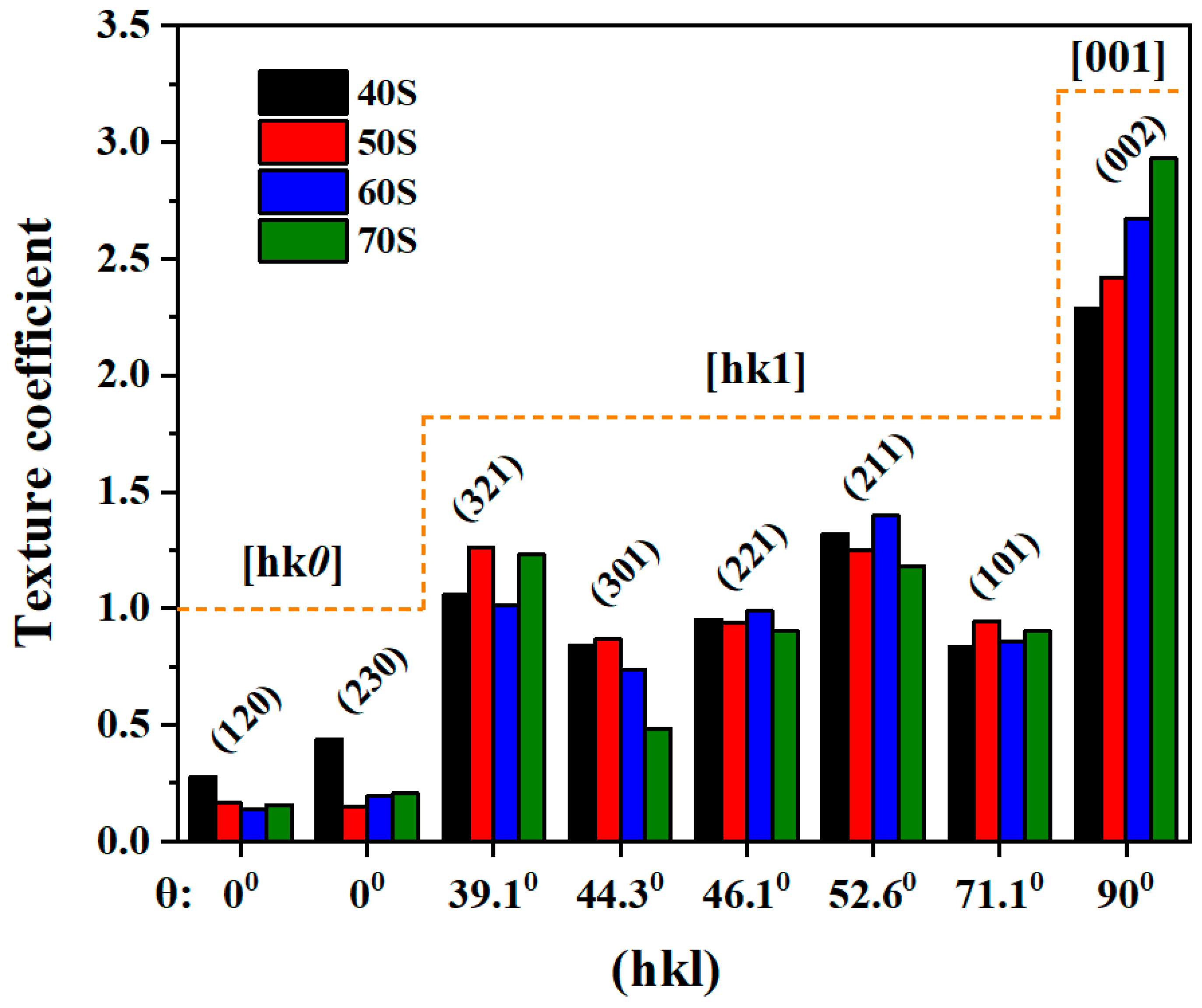
In order to further investigate the effect of deposition time on the texture and preferred orientation of Sb2Se3 films, the study also investigated the texture coefficient (TC) values for different crystalline surfaces (hkl). Exploring the TC of various crystallographic planes in Sb2Se3 thin films uncovered trends in crystal orientation changes during the film growth process. This investigation provided critical theoretical groundwork for optimizing the optoelectronic properties and application development of Sb2Se3 thin films. The texture coefficients (TCs) of the (120), (230), (321), (301), (221), (211), (101) and (002) peaks were calculated using the following formula:
where I(hkl) denotes the intensity of the (hkl) grain, I0(hkl) denotes the corresponding intensity of the (hkl) plane in the standard powder diffraction data (JCPDS 15-0861), N denotes all number of diffraction peaks taken into consideration in the formula [46].
Figure 5 illustrates that as the deposition time of Sb2Se3 extends from 40 to 60 s, the orientations of TC(221) and TC(211) exhibit an upward trend. Upon reaching 70 s, the TC(002) orientation of the Sb2Se3 film peaks, accompanied by a decline in the TC(221) and TC(211) orientations. Additionally, it is observed that the TC(101) orientation gradually surpasses 1, indicating a potential reorientation of the (Sb4Se6)n nanoribbons within the film as crystallinity improves. A portion of the (h0l) crystallographic plane undergoes a shift toward the preferred orientation, while the predominance of the (002) crystallographic plane persists. However, the diffraction peak weaving coefficients of the (211) and (221) crystallographic planes diminish. These findings suggest that optimizing the deposition time enhances the crystallinity and grain size of the films, fostering a more pronounced (hk1) preferred orientation. Consequently, Sb2Se3 films exhibit superior properties when deposited for 60 s.
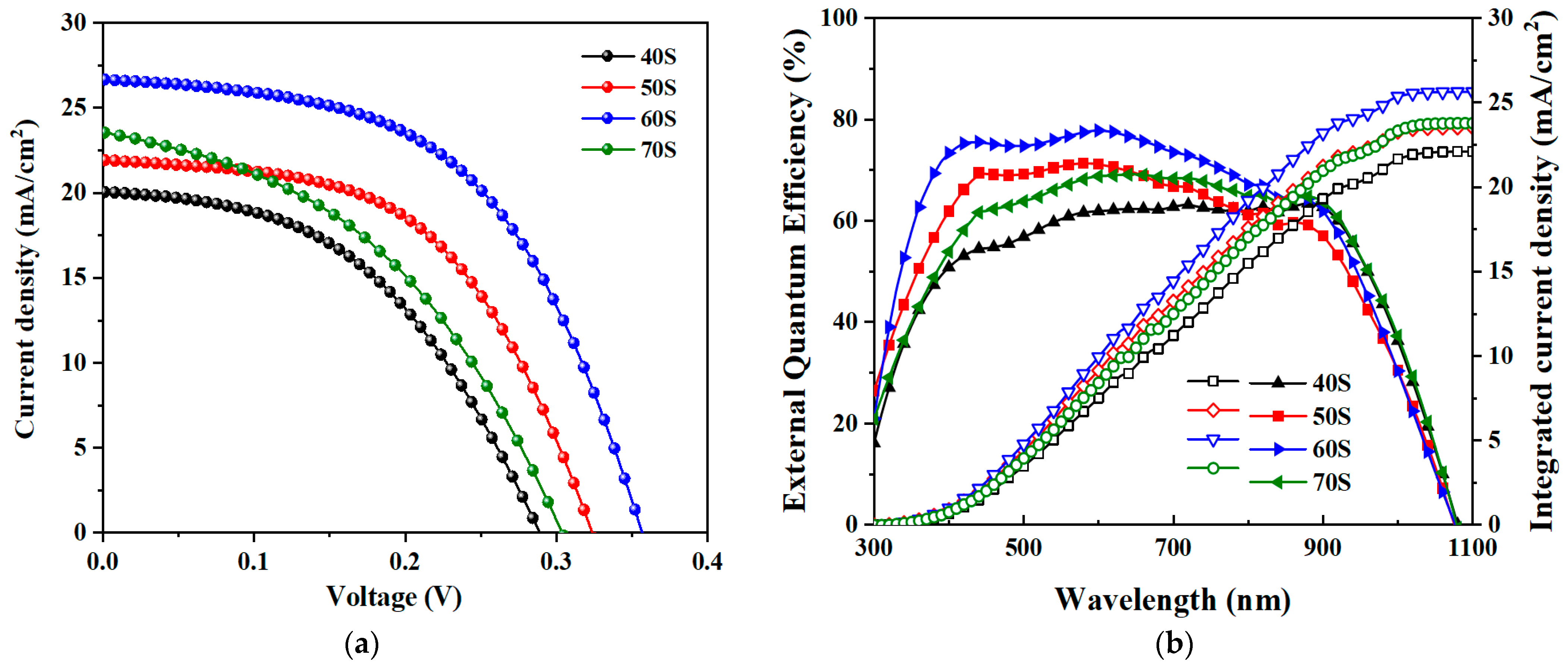
According to the above evaporation time study, the Sb2Se3 films were characterized by high crystallinity and preferred (hk1) orientation at an evaporation time of 60 s. As a result, Sb2Se3 solar cells with FTO/SnO2/Sb2Se3/P3HT/C device structure were prepared, and the J-V curves of the devices are shown in Figure 6a. As the crystallinity and structural integrity of the Sb2Se3 thin films reach an ideal state at 60 s, the device performance gains significant improvement in terms of charge transport as well as interface matching. The (hk1) optimally oriented grains result in a more ordered and stable structure in the grain boundary region, which leads to a lower surface energy of the grain boundaries, and the obtained Sb2Se3 grains grown on the substrate along the perpendicular direction are conducive to the reduction of interfacial compounding and absorption of transport losses. Table 2 shows the photovoltaic parameters of Sb2Se3 thin-film solar cells with different deposition times.
In particular, the increase in evaporation time from 40 s to 60 s, the decrease in series resistance (RS) from 79.56 Ω to 54.72 Ω, and the increase in parallel resistance (Rsh) from 2379.4 Ω to 4556.2 Ω can be attributed to the fact that an increase in the (hk1)-orientation ratio of the Sb2Se3 photoreactive layer enhances the longitudinal conductivity, which explains the corresponding enhancement in FF. The optimum photoelectric conversion efficiency of 5.06% was obtained for the device under this condition. Whereas the performance degradation of the devices with an evaporation time greater than 60 s may be attributed to the shift of the (101) crystallographic facets of the Sb2Se3 films to selective growth, the additional defects introduced by the nonessential crystallographic facets introduce energy at the surface of the grain boundaries, leading to an increase in the surface energy. The device Voc decreases to 0.244 V and the Jsc decreases to 19.86 mA/cm2. In addition, (002) peak strength selectivity implies that the longitudinal grains perpendicular to the substrate have the largest percentage of grains, and the larger intergranular voids and surface roughness give the films high interfacial defects. Furthermore, the increased surface roughness was likely detrimental to the interface characteristics between Sb2Se3 and P3HT. All these factors contributed to an increase in J0 (reverse saturation current), which in turn led to a reduction in the FF from 53.76% to 44.00%.
The broad response of all devices in the range of 350–1050 nm can be seen from the EQE spectra in Figure 6b, with the 60s device obtaining an EQE maximum of 78% at 610 nm. The EQE integral currents measured in the AM1.5 spectra are in very good agreement with Jsc. In addition, the effect of longitudinal optimization on the device is reflected in the significantly improved short-wave response, whereas the EQE mapping shows that the integration current of the Sb2Se3 thin-film device decreases sharply in the wavelength range of 400~800 nm. This suggests that as the evaporation time increases, when carriers encounter voids during their movement, they may be blocked or trapped in the voids. The carriers are conducted through the jumps between the lattices, which leads to the restriction of the carrier flow, causing the gradual degradation of the various device performances. This defect was primarily concentrated at the rear end of the absorber layer, leading to significant recombination of photogenerated carriers in this area. Consequently, the spectral response in the mid and long wavelengths was reduced, resulting in a decrease in both the FF and Jsc of the device, thereby diminishing the device’s performance.
Further, we simulated and fitted the results of J-V curves and EQE curves for Sb2Se3 devices with different deposition times (50 s, 60 s, 70 s) in Figure 6. For all fitted samples, the simulated J-V curves are slightly higher than the experimental data, which may indicate a slight idealization of the parameters assumed by the model. The simulated short-circuit current density was slightly lower than the experimental data, while the simulated open-circuit voltage was marginally higher than the experimental results. This indicated that there were discrepancies in the absorption coefficient, the rate of electron-hole pair generation, or transport properties considered in the simulation compared to the experimental conditions. Consequently, the photovoltaic performance of the device post-simulation fitting was slightly optimistic relative to the experimental outcomes. For the champion device with a deposition time of 60 s that was mentioned earlier, the simulation curves exhibited good agreement with the experimental data, suggesting that the mechanisms for photogenerated carrier capture and recombination considered in the simulation might have closely mirrored the experimental conditions, with carrier recombination losses at interfaces being minimized. Furthermore, as observed from Figure 7b, the consistency between experimental data and simulation was better in the short-wavelength region, aligning the model’s assumptions with the actual absorption and conversion efficiency of that spectral part. However, in the long-wavelength region, particularly beyond 800 nm, the divergence became more pronounced. The increase in the thickness of the Sb2Se3 absorption layer, accompanied by an increase in defects within the Sb2Se3 film, likely led to exacerbated carrier recombination, as reflected by the reduced EQE in the 400~750 nm wavelength range, suggesting significant carrier recombination within the absorber layer. This deviation corresponded to the previous analysis of Sb2Se3 crystal growth in experimental preparation.
The experimental results of J-V and EQE curves align with theoretical simulations, confirming that an optimal thickness of the absorptive layer ensures both high absorbance and the establishment of a robust built-in electric field with low defect density, thus yielding high photovoltaic conversion efficiency. Consequently, meticulously controlling the thickness of Sb2Se3 films via the CSS technique produces high-quality films with a preferred (hk1) orientation, enhancing the photovoltaic performance of Sb2Se3 solar cells.
4. Conclusions
In this study, Sb2Se3 thin films were successfully prepared using the close-space sublimation method, and precise control of film thickness and crystallization quality was achieved, based on which solar cell devices with FTO/SnO2/Sb2Se3/P3HT/C structures were prepared. The effects of deposition time on the crystal structure, morphology and optical properties of Sb2Se3 films were systematically investigated, and the formation mechanism of (hk1)-oriented Sb2Se3 films was thoroughly discussed. The results show that a reasonable deposition time can regulate the growth process of (Sb4Se6)n nanoribbons and make them grow in an orderly manner along the (hk1) crystallographic direction. The efficiency of photovoltaic devices made of high-quality Sb2Se3 films based on the (hk1) orientation is significantly improved, and an optimal device with a PCE of 5.06% is finally realized. However, prolonged deposition time leads to additional defects in grains with non-desired orientation, which affect carrier transport and lifetime, thus degrading device performance. In addition, we simulated and validated the experimental data of Sb2Se3 solar cells using wxAMPS software to further confirm the scientific validity and credibility of the conclusions drawn from the experiments, thus providing theoretical support for the related research. This work highlights the significant potential of the CSS technique in fabricating photovoltaic thin films with precise crystal orientations. It offers implications not only for advancing high-performance photovoltaic devices through close-space sublimation methods but also for inspiring novel ideas and directions in future photovoltaic material and device design.
Author Contributions
Writing—original draft, J.Z.; Writing—review & editing, J.Z. and S.L. All authors have read and agreed to the published version of the manuscript.
Funding
This research received no external funding.
Data Availability Statement
The original contributions presented in the study are included in the article, further inquiries can be directed to the corresponding authors.
Conflicts of Interest
The authors declare no conflicts of interests.
References
- Luo, Y.; Chen, G.; Chen, S.; Ahmad, N.; Azam, M.; Zheng, Z.; Su, Z.; Cathelinaud, M.; Ma, H.; Chen, Z.; et al. Carrier transport enhancement mechanism in highly efficient antimony selenide thin-film solar cell. Adv. Funct. Mater. 2023, 33, 2213941. [Google Scholar] [CrossRef]
- Fang, X.; Xie, L.; Li, X. Distributed localization in dynamic networks via complex laplacian. Automatica 2023, 151, 110915. [Google Scholar] [CrossRef]
- Lee, T.D.; Ebong, A.U. A review of thin film solar cell technologies and challenges. Renew. Sustain. Energy Rev. 2017, 70, 1286–1297. [Google Scholar] [CrossRef]
- Han, G.; Zhang, S.; Boix, P.P.; Wong, L.H.; Sun, L.; Lien, S.Y. Towards high efficiency thin film solar cells. Prog. Mater. Sci. 2017, 87, 246–291. [Google Scholar] [CrossRef]
- Fang, X.; Xie, L. Distributed Formation Maneuver Control Using Complex Laplacian. IEEE Trans. Autom. Control. 2023, 69, 1850–1857. [Google Scholar] [CrossRef]
- Pal, K.; Singh, P.; Bhaduri, A.; Thapa, K.B. Current challenges and future prospects for a highly efficient (>20%) kesterite CZTS solar cell: A review. Sol. Energy Mater. Sol. Cells 2019, 196, 138–156. [Google Scholar] [CrossRef]
- Britt, J.; Ferekides, C. Thin-film CdS/CdTe solar cell with 15.8% efficiency. Appl. Phys. Lett. 1993, 62, 2851–2852. [Google Scholar] [CrossRef]
- Green, M.A.; Ho-Baillie, A.; Snaith, H.J. The emergence of perovskite solar cells. Nat. Photonics 2014, 8, 506–514. [Google Scholar] [CrossRef]
- Doumit, N.; Soro, K.; Ozocak, A.; Batut, N.; Schellmanns, A.; Saintaime, E.; Ntsoenzok, E. Boosting the efficiency of CZTS/Si tandem solar cells using In2O3 layer in CZTS top cell. Adv. Theory Simul. 2021, 4, 2100099. [Google Scholar] [CrossRef]
- Shi, Z.; Jayatissa, A.H. Perovskites-based solar cells: A review of recent progress, materials and processing methods. Materials 2018, 11, 729. [Google Scholar] [CrossRef]
- Barbato, M.; Artegiani, E.; Bertoncello, M.; Meneghini, M.; Trivellin, N.; Mantoan, E.; Romeo, A.; Mura, G.; Ortolani, L.; Zanoni, E.; et al. CdTe solar cells: Technology, operation and reliability. Phys. D Appl. Phys. 2021, 54, 333002. [Google Scholar] [CrossRef]
- Gonzalez-Pedro, V.; Juarez-Perez, E.J.; Arsyad, W.S.; Barea, E.M.; Fabregat-Santiago, F.; Mora-Sero, I.; Bisquert, J. General working principles of CH3NH3PbX3 perovskite solar cells. Nano Lett. 2014, 14, 888–893. [Google Scholar] [CrossRef]
- Wang, L.; Li, D.B.; Li, K.; Chen, C.; Deng, H.X.; Gao, L.; Zhao, Y.; Jiang, F.; Li, L.; Huang, F.; et al. Stable 6%-efficient Sb2Se3 solar cells with a ZnO buffer layer. Nat. Energy 2017, 2, 17046. [Google Scholar] [CrossRef]
- Duan, Z.; Liang, X.; Feng, Y.; Ma, H.; Liang, B.; Wang, Y.; Luo, S.; Wang, S.; Schropp, R.E.I.; Mai, Y.; et al. Sb2Se3 Thin-Film Solar Cells Exceeding 10% Power Conversion Efficiency Enabled by Injection Vapor Deposition Technology. Adv. Mater. 2022, 34, 2202969. [Google Scholar] [CrossRef] [PubMed]
- Choi, Y.C.; Mandal, T.N.; Yang, W.S.; Lee, Y.H.; Im, S.H.; Noh, J.H.; Seok, S.I. Sb2Se3-sensitized inorganic–organic heterojunction solar cells fabricated using a single-source precursor. Angew. Chem. 2014, 126, 1353–1357. [Google Scholar] [CrossRef]
- Tao, J.; Hu, X.; Xue, J.; Wang, Y.; Weng, G.; Chen, S.; Zhu, Z.; Chu, J. Investigation of electronic transport mechanisms in Sb2Se3 thin-film solar cells. Sol. Energy Mater. Sol. Cells 2019, 197, 1–6. [Google Scholar] [CrossRef]
- Lin, J.; Chen, G.; Ahmad, N.; Ishaq, M.; Chen, S.; Su, Z.; Fan, P.; Zhang, Y.; Liang, G. Back contact interfacial modification mechanism in highly-efficient antimony selenide thin-film solar cells. J. Energy Chem. 2023, 80, 256–264. [Google Scholar] [CrossRef]
- Phillips, L.J.; Savory, C.N.; Hutter, O.S.; Yates, P.J.; Shiel, H.; Mariotti, S.; Bowen, L.; Birkett, M.; Durose, K.; Major, J.D. Current enhancement via a TiO2 window layer for CSS Sb2Se3 solar cells: Performance limits and high VOC. IEEE J. Photov. 2018, 9, 544–551. [Google Scholar] [CrossRef]
- Razykov, T.M.; Shukurov, A.X.; Atabayev, O.K.; Kuchkarov, K.M.; Ergashev, B.; Mavlonov, A.A. Growth and characterization of Sb2Se3 thin films for solar cells. Sol. Energy 2018, 173, 225–228. [Google Scholar] [CrossRef]
- Zeng, Y.; Sun, K.; Huang, J.; Nielsen, M.P.; Ji, F.; Sha, C.; Yuan, S.; Zhang, X.; Yan, C.; Liu, X.; et al. Quasi-vertically-orientated antimony sulfide inorganic thin-film solar cells achieved by vapor transport deposition. ACS Appl. Mater. Interfaces 2020, 12, 22825–22834. [Google Scholar] [CrossRef]
- AvGarcía, R.G.A.; Cerdán-Pasarán, A.; Madrigal, A.F.; Mathews, N.R. Antimony Selenide Thin Films by Electrodeposition: Influence of Deposition Conditions and Post-Deposition Thermal Treatment on Physical and Photoelectrochemical Properties. Phys. Status Solidi (A) 2022, 219, 2200185. [Google Scholar]
- Brito, D.; Anacleto, P.; Pérez-Rodríguez, A.; Fonseca, J.; Santos, P.; Alves, M.; Cavalli, A.; Sharma, D.; Claro, M.S.; Nicoara, N.; et al. Antimony Selenide Solar Cells Fabricated by Hybrid Reactive Magnetron Sputtering. Nanomaterials 2023, 13, 2257. [Google Scholar] [CrossRef] [PubMed]
- Chen, G.J.; Tang, R.; Chen, S.; Zheng, Z.H.; Su, Z.H.; Ma, H.L.; Zhang, X.H.; Fan, P.; Liang, G.X. Crystal growth promotion and defect passivation by hydrothermal and selenized deposition for substrate-structured antimony selenosulfide solar cells. ACS Appl. Mater. Interfaces 2022, 14, 31986–31997. [Google Scholar] [CrossRef] [PubMed]
- Eensalu, J.S.; Tonsuaadu, K.; Acik, I.O.; Krunks, M. Sb2S3 thin films by ultrasonic spray pyrolysis of antimony ethyl xanthate. Mater. Sci. Semicond. Process. 2022, 137, 106209. [Google Scholar] [CrossRef]
- Wang, X.; Tang, R.; Yin, Y.; Ju, H.; Zhu, C.; Chen, T. Interfacial engineering for high efficiency solution processed Sb2Se3 solar cells. Sol. Energy Mater. Sol. Cells 2019, 189, 5–10. [Google Scholar] [CrossRef]
- Paudel, N.R.; Grice, C.R.; Xiao, C.; Yan, Y. High temperature CSS processed CdTe solar cells on commercial SnO2: F/SnO2 coated soda-lime glass substrates. J. Mater. Sci. Mater. Electron. 2015, 26, 4708–4715. [Google Scholar] [CrossRef]
- Lin, J.; Mahmood, A.; Chen, G.; Ahmad, N.; Chen, M.; Fan, P.; Chen, S.; Tang, R.; Liang, G. Crystallographic orientation control and defect passivation for high-efficient antimony selenide thin-film solar cells. Mater. Today Phys. 2022, 27, 100772. [Google Scholar] [CrossRef]
- Zhou, H.; Feng, M.; Song, K.; Bin, L.; Wang, Y.; Liu, R.; Gong, X.; Zhang, D.; Cao, L.; Chen, S. A highly [001]-textured Sb2Se3 photocathode for efficient photoelectrochemical water reduction. Nanoscale 2019, 11, 22871–22879. [Google Scholar] [CrossRef]
- Li, Z.; Liang, X.; Li, G.; Liu, H.; Zhang, H.; Guo, J.; Chen, J.; Shen, K.; San, X.; Yu, W. 9.2%-efficient core-shell structured antimony selenide nanorod array solar cells. Nat. Commun. 2019, 10, 125. [Google Scholar] [CrossRef]
- Singh, Y.; Maurya, K.K.; Singh, V.N. A review on properties, applications, and deposition techniques of antimony selenide. Sol. Energy Mater. Sol. Cells 2021, 230, 111223. [Google Scholar]
- Wang, W.; Cao, Z.; Wu, L.; Liu, F.; Ao, J.; Zhang, Y. Remarkable Sb2Se3 solar cell with a carbon electrode by tailoring film growth during the VTD process. ACS Appl. Energy Mater. 2021, 4, 13335–13346. [Google Scholar] [CrossRef]
- Tao, R.; Tan, T.; Zhang, H.; Meng, Q.; Zha, G. Sb2Se3 solar cells fabricated via close-space sublimation. J. Vac. Sci. Technol. B 2021, 39, 052203. [Google Scholar] [CrossRef]
- Rijal, S.; Li, D.B.; Awni, R.A.; Bista, S.S.; Song, Z.; Yan, Y. Influence of post-selenization temperature on the performance of substrate-type Sb2Se3 solar cells. ACS Appl. Energy Mater. 2021, 4, 4313–4318. [Google Scholar] [CrossRef]
- Fan, P.; Chen, G.J.; Chen, S.; Zheng, Z.H.; Azam, M.; Ahmad, N.; Su, Z.H.; Liang, G.H.; Zhang, X.-H.; Chen, Z.G. Quasi-vertically oriented Sb2Se3 thin-film solar cells with open-circuit voltage exceeding 500 mV prepared via close-space sublimation and selenization. ACS Appl. Mater. Interfaces 2021, 13, 46671–46680. [Google Scholar] [CrossRef] [PubMed]
- Yu, C.; Xin-Yun, Z.; Han-Bo, C.; Wang, C.G.; Zhang, X.T.; Hou, B.D.; Shen, M.R.; Jing, Z. Simulation and optimal design of antimony selenide thin film solar cells. Acta Phys. Sin. 2018, 67, 247301. [Google Scholar]
- Memari, A.; Javadian Sarraf, M.; Seyyed Mahdavi Chabok, S.J.; Motevalizadeh, L. Comprehensive guidance for optimizing the colloidal quantum dot (CQD) Perovskite solar cells: Experiment and simulation. Sci. Rep. 2023, 13, 16675. [Google Scholar] [CrossRef] [PubMed]
- Barthwal, S.; Gupta, R.; Kumar, A.; Ramesh, K.; Pathak, S.; Karak, S. Band offset engineering in antimony sulfide (Sb2S3) solar cells, using SCAPS simulation: A route toward PCE > 10%. Optik 2023, 282, 170868. [Google Scholar] [CrossRef]
- Teimouri, R.; Keshtmand, R.; Mehrvarz, S.; Ghasemi, F.; Mahjoory, A.; Kolahdouz, M.; Taghavinia, N. Enhancing Planar Perovskite Solar Cell Performance by SnO2 Interface Treatment Using Urea as an Additive: A Comparative Study of Simple, Low-Temperature Approaches. ACS Appl. Electron. Mater. 2023, 5, 6014–6025. [Google Scholar] [CrossRef]
- Salem, M.S.; Shaker, A.; Abouelatta, M.; Alanazi, A.; Al-Dhlan, K.A.; Almurayziq, T.S. Numerical analysis of hole transport layer-free antimony selenide solar cells: Possible routes for efficiency promotion. Opt. Mater. 2022, 129, 112473. [Google Scholar] [CrossRef]
- Karimi, E.; Ghorashi, S.M.B. Simulation of perovskite solar cell with P3HT hole-transporting materials. J. Nanophotonics 2017, 11, 032510. [Google Scholar] [CrossRef]
- Chen, C.; Zhao, Y.; Lu, S.; Li, K.; Yang, B.; Chen, W.; Wang, K.; Li, D.; Deng, H.; Yi, F.; et al. Accelerated optimization of TiO2/Sb2Se3 thin film solar cells by high-throughput combinatorial approach. Adv. Energy Mater. 2017, 7, 1700866. [Google Scholar] [CrossRef]
- Chen, C.; Wang, L.; Gao, L.; Nam, D.; Li, D.; Li, K.; Zhao, Y.; Ge, C.; Cheong, H.; Liu, H.; et al. 6.5% certified efficiency Sb2Se3 solar cells using PbS colloidal quantum dot film as hole-transporting layer. ACS Energy Lett. 2017, 2, 2125–2132. [Google Scholar] [CrossRef]
- Wen, X.; Chen, C.; Lu, S.; Li, K.; Kondrotas, R.; Zhao, Y.; Chen, W.; Gao, L.; Wang, C.; Zhang, J.; et al. Vapor transport deposition of antimony selenide thin film solar cells with 7.6% efficiency. Nat. Commun. 2018, 9, 2179. [Google Scholar] [CrossRef] [PubMed]
- Zhou, J.; Chen, H.; Zhang, X.; Chi, K.; Cai, Y.; Cao, Y.; Pang, J. Substrate dependence on (Sb4Se6)n ribbon orientations of antimony selenide thin films: Morphology, carrier transport and photovoltaic performance. J. Alloys Compd. 2021, 862, 158703. [Google Scholar] [CrossRef]
- Chen, G.; Li, X.; Abbas, M.; Fu, C.; Su, Z.; Tang, R.; Chen, S.; Fan, P.; Liang, G. Tellurium doping inducing defect passivation for highly effective antimony selenide thin film solar cell. Nanomaterials 2023, 13, 1240. [Google Scholar] [CrossRef]
- Karade, V.C.; Jang, J.S.; Kumbhar, D.; Rao, M.; Pawar, P.S.; Kim, S.; Gour, K.S.; Park, J.; Heo, J.; Dongale, T.D.; et al. Combating open circuit voltage loss in Sb2Se3 solar cell with an application of SnS as a back surface field layer. Sol. Energy 2022, 233, 435–445. [Google Scholar] [CrossRef]
Figure 1.
(a) Transmission spectra of FTO films and FTO:SnO2 films; (b) Structure of the studied Sb2Se3 solar cell; (c) Schematic diagram of the CSS technique to deposit Sb2Se3 film.
Figure 1.
(a) Transmission spectra of FTO films and FTO:SnO2 films; (b) Structure of the studied Sb2Se3 solar cell; (c) Schematic diagram of the CSS technique to deposit Sb2Se3 film.

Figure 2.
Comparative analysis between the experimental and simulated results of the highest efficiency Sb2Se3 devices: (a) J-V curves; (b) EQE curves.
Figure 2.
Comparative analysis between the experimental and simulated results of the highest efficiency Sb2Se3 devices: (a) J-V curves; (b) EQE curves.

Figure 3.
SEM images of Sb2Se3 thin films prepared with optimized deposition times under the conditions of (a,e) 40 s, (b,f) 50 s, (c,g) 60 s, and (d,h) 70 s.
Figure 3.
SEM images of Sb2Se3 thin films prepared with optimized deposition times under the conditions of (a,e) 40 s, (b,f) 50 s, (c,g) 60 s, and (d,h) 70 s.

Figure 4.
The XRD patterns of the Sb2Se3 films synthesized at different deposition times.

Figure 5.
Texture coefficient of the Sb2Se3 films synthesized at different deposition times.

Figure 6.
Sb2Se3 thin-film solar cells at different deposition times: (a) J-V curves; (b) EQE curves.
Figure 6.
Sb2Se3 thin-film solar cells at different deposition times: (a) J-V curves; (b) EQE curves.

Figure 7.
Experimental and simulation comparison of Sb2Se3 thin-film solar cells with different deposition times: (a) J-V curves; (b) EQE curves.
Figure 7.
Experimental and simulation comparison of Sb2Se3 thin-film solar cells with different deposition times: (a) J-V curves; (b) EQE curves.


| Parameter | SnO2 | Sb2Se3 | P3HT |
|---|---|---|---|
| Thickness (nm) | 50 | 500 | 50 |
| Relative permittivity (εr) | 9 | 10 | 10 |
| Electron affinity, Χ (eV) | 4.5 | 4.04 | 4 |
| Electron mobility, μn (cm2/Vs) | 0.2 | 4 | 0.006 |
| Hole mobility, μp (cm2/Vs) | 0.2 | 0.1 | 0.006 |
| Na (1/cm3) | 0 | 1 × 10¹³ | 5 × 10¹⁹ |
| Nd (1/cm3) | 1 × 10¹⁸ | 0 | 0 |
| Nt (1/cm3) | 1 × 10¹⁸ | 2 × 10¹⁶ | 1 × 10¹⁷ |
| Eg (eV) | 3.6 | 1.2 | 3.2 |
| Density of state of the conduction band, Nc (1/cm3) | 2.2 × 10¹⁸ | 2.2 × 10¹⁸ | 1.0 × 10²¹ |
| Density of state of the valence band, Nv (l/cm3) | 1.8 × 10¹⁹ | 1.8 × 10¹⁹ | 2.0 × 10²⁰ |
Table 2.
Photovoltaic parameters of Sb2Se3 thin-film solar cells at different deposition times.
| Deposition Time (s) | Voc (V) | Jsc (mA/cm2) | FF (%) | PCE (%) | Rs (Ω) | Rsh (Ω) |
|---|---|---|---|---|---|---|
| 40 | 0.284 | 20.05 | 47.43 | 2.704 | 79.56 | 2379.4 |
| 50 | 0.318 | 22.01 | 54.19 | 3.794 | 63.55 | 4465.1 |
| 60 | 0.352 | 26.79 | 53.76 | 5.067 | 54.72 | 4556.2 |
| 70 | 0.295 | 23.51 | 44.00 | 3.047 | 81.85 | 829.52 |
Disclaimer/Publisher’s Note: The statements, opinions and data contained in all publications are solely those of the individual author(s) and contributor(s) and not of MDPI and/or the editor(s). MDPI and/or the editor(s) disclaim responsibility for any injury to people or property resulting from any ideas, methods, instructions or products referred to in the content. |
© 2024 by the authors. Licensee MDPI, Basel, Switzerland. This article is an open access article distributed under the terms and conditions of the Creative Commons Attribution (CC BY) license (https://creativecommons.org/licenses/by/4.0/).
Share and Cite
MDPI and ACS Style
Zhang, J.; Li, S. The Effect of Deposition Time Optimization on the Photovoltaic Performance of Sb2Se3 Thin-Film Solar Cells. Energies 2024, 17, 1937. https://doi.org/10.3390/en17081937
AMA Style
Zhang J, Li S. The Effect of Deposition Time Optimization on the Photovoltaic Performance of Sb2Se3 Thin-Film Solar Cells. Energies. 2024; 17(8):1937. https://doi.org/10.3390/en17081937
Chicago/Turabian StyleZhang, Jie, and Shanze Li. 2024. "The Effect of Deposition Time Optimization on the Photovoltaic Performance of Sb2Se3 Thin-Film Solar Cells" Energies 17, no. 8: 1937. https://doi.org/10.3390/en17081937
Note that from the first issue of 2016, this journal uses article numbers instead of page numbers. See further details here.