A Parameter Optimization Design Method for Single-Phase Dual Active Bridge AC-DC Converter


School of Electrical Engineering, Chongqing University, Chongqing 400044, China
*
Author to whom correspondence should be addressed.
Energies 2024, 17(8), 1955; https://doi.org/10.3390/en17081955
Submission received: 5 April 2024
/
Revised: 16 April 2024
/
Accepted: 17 April 2024
/
Published: 19 April 2024
(This article belongs to the Section F3: Power Electronics)
Abstract
:The single-stage dual active bridge (DAB) AC-DC converter has the advantages of high power density, low cost, and simple control; it has a broad potential for application in the field of onboard chargers (OBC). However, the lack of fast and accurate quantitative parameter optimization design methods in single-stage DAB AC-DC converters limits the overall efficiency of the converter. Based on the above problem, in order to improve the overall operating efficiency of the converter by optimizing the parameter transformer ratio and power inductance, this paper proposes a parameter design method considering a multi-timescale strategy by combining the steady-state analysis model of the converter in the line cycle and switching cycle and step-by-step reducing its design space through the constraints on the parameters. The first step is to obtain a safe design space for the parameters under the converter’s transmitted power and current stress constraints. The second step obtains the optimization design space of the parameters under the optimization of conduction loss and switching loss of the converter. Finally, the optimal parameters are determined by the loss analysis model. The proposed parameter optimization method entirely takes into account the steady-state characteristics of the DAB AC-DC converter during the line cycle, and the step-by-step constraints greatly accelerate the parameter design process. In addition, the proposed parameter optimization design method applies to all types of single-stage DAB AC-DC converters, which can be well applied to engineering practice.
1. Introduction
Single-stage dual active bridge (DAB) AC-DC converters have more potential in terms of efficiency, reliability, and power density due to the single-stage power conversion, which eliminates the use of large-capacity electrolytic capacitors on the DC bus [1,2,3,4,5]; instead, they have a promising future in the fields of on-board chargers, energy storage systems, and DC power distribution systems [6]. Numerous single-stage DAB AC-DC converter topologies have been proposed in existing research, and in particular, a totem pole-type DAB AC-DC converter is introduced in ref. [7], which employs a totem pole bridgeless rectifier structure on the AC side and multiplexes the high-frequency bridge arms in the rectifier with the primary-side bridge arms of the DAB converter. This further reduces switches and converter losses, giving it an advantage over single-stage DAB AC-DC converter topologies.
Due to the single-stage power conversion of the single-stage DAB AC-DC converter, the input voltage to the converter is a rectified sine wave, resulting in the converter usually operating over an extensive voltage gain range. Therefore, the research on single-stage DAB AC-DC converters mainly focuses on optimizing the modulation strategy to improve the converter’s efficiency over an ultra-wide voltage gain range [8,9,10]. However, from the steady-state analysis model of the DAB converter, it can be seen that the steady-state performance of the converter is also affected by its circuit parameters. Therefore, it isn’t easy to fully improve the converter’s performance only through optimizing the modulation strategy. Based on this, to realize the synchronous optimization by combining hardware and software to improve the overall efficiency of the converter further, this paper proposes a parameter optimization design method for the single-stage DAB AC-DC converter.
The parameter design method of the DAB converter has been studied in related literature. In ref. [11], the voltage gain of the converter with the highest operating efficiency is obtained by solving the problem under single phase-shift modulation by considering the actual operating condition of the DAB converter and the modulation strategy. Then the optimal design of the transformer ratio is obtained. However, this method only optimizes the transformer ratio without considering the optimal design of the power inductor. In ref. [12], the optimal parameters are obtained by iterative numerical computation based on the loss model, and the optimal design method can get the exact solution. However, due to the complexity of the loss model, the calculation time of the algorithm is long, and the optimization effect depends on the accuracy of the loss model, so it isn’t easy to apply in engineering. In ref. [13], the discrete design strategy is used to optimize the parameters, but the method assumes that the transformer ratio is 1, so it does not have the generality. In ref. [14], a numerical method is used to obtain the optimal parameters by minimizing the inductor RMS current under the TPS modulation scheme. However, this method consumes a lot of time through numerical search. In ref. [15], an accurate frequency domain steady-state model of the DAB converter is developed, based on which the loss model of the converter is derived, and then the total loss is optimized by particle swarm optimization algorithm to obtain the optimal parameters.
The proposed parametric design methods mentioned above are based on the DAB DC-DC converter. Therefore, only the waveforms of a single switching cycle for a specific operating condition are considered in the design. For the DAB AC-DC converter, the operating waveforms of each switching cycle in the line cycle are inconsistent due to the frequency variations of the input voltage and the transferred power, and the operating waveforms of a single switching cycle cannot reflect the steady-state operation of the converter. More importantly, the above differences lead to a highly complex loss model for the DAB AC-DC converter, and it is difficult to establish the loss analysis model of the converter under a single switching cycle like the DAB DC-DC converter.
Therefore, compared with the existing design methods, this paper explores the parameter design method of the DAB AC-DC converter, concerning its multi-timescale steady-state operating characteristics for the first time. The proposed parameter design method combines the operating waveforms of the converter in the line cycle and switching cycle and seeks the optimization of transformer ratio and power inductance within the design space of the determined parameters to further improve the overall operating efficiency of the single-stage DAB AC-DC converter.
The rest of the paper is organized as follows. Section 2 presents the analysis of the multi-timescale steady state of the DAB AC-DC converter and the idea of a step-by-step design approach. A safe design space for the parameters is established from the constraints of output power and inductor current stresses in Section 3. In Section 4, an optimized design space for the parameters is established by exploring the effect of the parameters on the conduction loss and switching loss of the converter. In Section 5, the optimal parameter combinations are determined based on the converter loss analysis model. In Section 6, the scheme’s effectiveness is verified by an experimental prototype. Finally, conclusions are drawn in Section 7.
2. Parameter Optimization Design Framework for DAB AC-DC Converter
2.1. Multi-Timescale Steady-State Analysis of the DAB AC-DC Converter
The topology of the totem pole type DAB AC-DC converter is shown in Figure 1. It consists of a totem pole bridgeless rectifier and a DAB DC-DC converter with a small HF filter capacitor Cc in the middle. Using the extended phase-shift (EPS) optimized modulation scheme proposed in ref. [16], the converter can be operated with guaranteed open-loop PFC and minimum circulating currents over the entire operating range, which ensures the performance of the converter at the control level for the same set of parameters.
The specifications of the converter designed in this paper are shown in Table 1; the RMS AC input voltage of the converter is 110 V, the output voltage Vs = 360~400 V, the switching frequency fs = 100 kHz, and the rated output power PN = 800 W. The MOSFET is chosen to be Rohm’s SCT3060AL, which has a drain-source voltage of 650 V and a drain current of 39 A, and it can satisfy the requirements of the converter’s steady-state operation.
The expression for the inductor current in each switching cycle can be obtained from the time-domain steady-state analytical model of the DAB AC-DC converter under EPS modulation. However, the steady-state characteristics of the line cycle of the DAB AC-DC converter result in different steady-state waveforms of the converter in each switching cycle. Therefore, in analyzing the characteristic quantities such as the peak inductor current during the steady-state operation of the DAB AC-DC converter, the inductor current waveform can’t be considered only during a single switching cycle. The steady-state waveforms of the converter during line cycle Tg and switching cycle Ts under EPS modulation are shown in Figure 2. The inductor-current waveform of the m th switching cycle of the DAB converter is determined by the input voltage Vp(m) and the transmitted power p(m) at the moment. where p(m) is:
where vg and ig are the AC input voltage and current, and iDAB is the average input current of the DAB converter. Since both Vp(m) and p(m) magnitudes vary with Tg/2, the peak inductor current, RMS value, and ZVS range for steady-state operation of the converter are analyzed over half a line cycle.
In ref. [16], the expression for the peak-to-peak inductor current Ipp of the DAB converter under EPS modulation is:
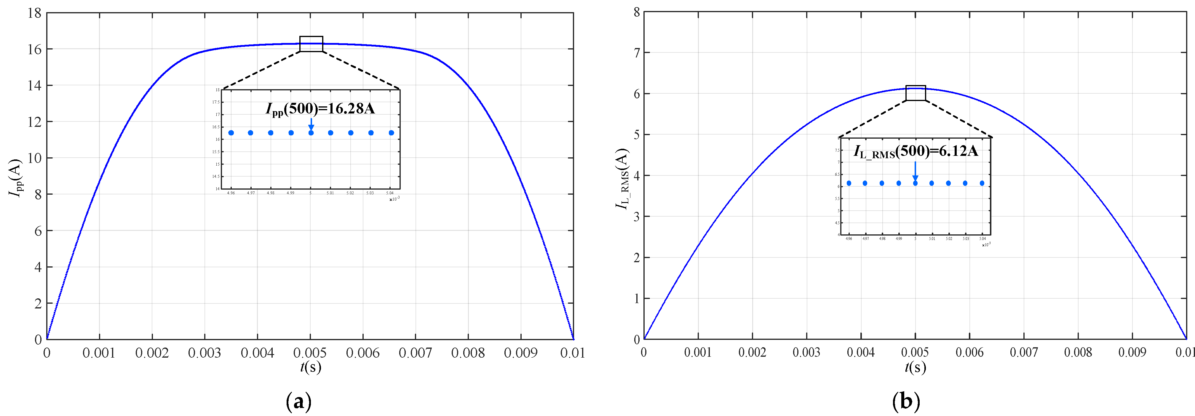
From Equation (2), the peak-to-peak inductor current Ipp for each switching cycle of the converter at operating condition (Vs = 400 V, P = 800 W) in Tg/2 with parameter N = 1 and Ls = 50 μH can be calculated, as shown in Figure 3a. Similarly, the inductor current RMS IL_RMS in each switching cycle can be obtained, as shown in Figure 3b.
From Figure 3, it can be seen that, for the single-stage DAB AC-DC converter, the Ipp and the IL_RMS are varied by switching cycle. Under the operating condition (400 V, 800 W), the maximum peak inductor current occurs at the 500th switching cycle (t = 0.005 s), when Ipp (500) = 16.28 A and the IL_RMS(500) = 6.12 A. Therefore, it cannot calculate the conduction loss of the converter for a specific operating condition based on the IL_RMS for a single switching cycle.
The ZVS range of the DAB AC-DC converter switch is analyzed below. For the DAB AC-DC converter, it is necessary to analyze at least (0.5Tg)/Ts = 1000 switching cycles by considering that the input voltage and the transmitted power vary periodically within Tg/2, which results in different ZVS realizations of the converter at each switching cycle. This complicates the determination of the range of ZVS realization during the steady-state operation of the DAB AC-DC converter.
The turn-on current of each switching tube in a totem pole DAB AC-DC converter with EPS modulation is calculated as follows:
From the above equation, iS1 and iS2 depends on the current of inductor Lg and inductor Ls. And the current of inductor Lg is:
And in the positive half-line cycle: ig > 0; in the negative half-line cycle: ig < 0, so the ZVS realizations of switch tubes S1 and S2 isn’t identical.
Due to the symmetry of the inductor currents in the switching cycles under EPS modulation, the ZVS realizations of switch S3 and S4, Q1 and Q2, and Q3, and Q4 are the same, so only the ZVS cases of switch S1, S2, S4, Q2, and Q4 need to be analyzed. In this section, the turn-on moment current values of each switch of the converter at operating conditions (400 V,800 W) are solved for the parameters N = 1 and Ls = 50 μH, as shown in Figure 4.
To simplify the ZVS analysis of the converter, it is considered that ZVS can be realized when the current of the switch at the turn-on moment is less than zero. As shown in Figure 4, the current at the opening moment of the switch S1 and S2 mainly depends on the AC current ig, so in the positive half-line cycle: S1 can realize ZVS and S2 hard-switching, and in the negative half-line cycle: S2 can realize ZVS and S1 hard-switching. The secondary switch Q1~Q4 can realize ZVS in the entire power region; the primary switch S3 and S4 can realize ZVS only in the high power region.
From the above analysis, the inductor current peak-to-peak Ipp, IRMS, and ZVS ranges of the converter are obtained in the line cycle. This is essential for the subsequent determination of the parameter design space of the converter and the calculation of the converter losses.
2.2. Parameter Optimization Design Framework
When the control method of the converter is determined, the next step is to design the hardware parameters of a converter. For the parameter design of the DAB AC-DC converter, there are the following steps: (1) Determine the specifications of the converter according to the application scenario; (2) Establish the switching cycle steady-state analysis model of the DAB converter; (3) Calculate the steady-state eigenvalue of the converter under the determined modulation scheme; (4) Design and optimize the parameters of the circuit under the solved steady-state eigenvalue; (5) Test the prototype of the converter.
For the DAB converter, the parameters to be designed are the transformer ratio N and the power inductance Ls. In practical operating conditions, the following constraints are essential to protect the safety and high efficiency of the converter: (1) the constraint of the transmission power: the parameters of the circuit enable the converter to reach the maximum transmission power requirement; (2) the constraint of the current stress: the main circuit parameters obtained by designing the current peak in the full-load condition should be less than the maximum value that the power device can withstand. The design area that satisfies the above two conditions is the safe design space. In addition, we consider that the parameter design results affect the inductor current RMS and ZVS range of the converter, which correspond to the conduction loss and switching loss of the converter, respectively, and thus affect the converter’s efficiency. Therefore, this paper explores the distribution of the RMS and ZVS ranges of the converter with different parameters N and Ls to narrow down the optimal parameter design region further, referred to as the optimal design space of the parameters.
In the following, each section is described in detail.
3. Safe Design Space for Parameters
3.1. Transmission Power Constraints
Ensuring that the parameters can guarantee the transferred power and voltage gain requirements of the converter is the first step in the parameter design. It allows a preliminary determination of the design region of the parameters to decrease the design space of parameters. From Table 1, the rated power of the converter is PN = 800 W. And the maximum transmission power of the converter under EPS modulation is:
Considering the 1/4 power margin for the converter design, it is required that the maximum transferred power of the converter is at least 5/4 of the rated power. Since the maximum value of the instantaneous transferred power of the AC-DC converter is twice the steady-state transferred power, the PM should be not less than 5/2 of the rated power:
Substituting the prototype parameters into Equation (4), the constraints satisfied between N and Ls can be calculated with:
According to the constraint of the transferred power, the relationship between the transformer ratio N and the power inductance Ls can be derived. Next, the range of transformer ratio N is solved. For a DAB converter, it is illustrated in ref. [17] that the closer the voltage gain M tends to 1, the smaller the return power and loop current and the higher the power transfer efficiency, where the voltage gain M = NVs/Vp. But for a single-stage DAB AC-DC converter, due to the input voltage Vp, the voltage gain M varies during the line cycle and tends to infinity at the zero-crossing point of Vp. Therefore, it can only be constrained to the minimum value of voltage gain Mmin, and the range of Mmin is:
To ensure that the voltage gain M under EPS modulation is always greater than 1, it is necessary to ensure that Mmin ≥ 1 and then get the lower limit of the transformer ratio N. Considering that a larger transformer ratio N will lead to a significant increase in the secondary current, it is set that N < 3. The range of the transformer ratio N is:
Therefore, the range of the transformer ratio N and power inductance Ls is constrained by Equations (5) and (7), and the range that satisfies the conditions can be obtained as shown in Figure 5. The yellow area in the figure is the effective range of the parameters N and Ls under the transmission power constraints, and within this range, the selected parameters are able to satisfy the requirements of the transmission power.
3.2. Current Stress Constraints
After determining the parameter range of the circuit under the transmission power constraint, the parameter design space under the current stress constraint needs to be considered. The current stress constraint ensures that the maximum current of the inductor is less than the maximum current that the switch can withstand. As shown in Figure 3a, the peak value of inductor current Ipp under specific operating conditions varies by switching cycle. Considering the two times margin of peak inductor current under EPS modulation, it is necessary to ensure that the maximum Ipp during the line cycle cannot exceed the current stress constraint.
Within the transmission power constraints shown in Figure 5, a set of randomly selected parameters N = 1.5 and Ls = 40 μH. The maximum inductor current peak-to-peak Ipp variation with the output power P versus the output voltage Vs can be obtained, as shown in Figure 6. The drain current of the selected switch SCT3060AL is 39 A. The Ipp allowed to flow in the whole power range of the switch on the secondary side is 39/1.5 = 26 A when N = 1.5. Therefore, when Ipp exceeds 26 A, i.e., the red region, it can be considered that the current stress constraint is not satisfied under these parameters.
To find a safe design space to satisfy the current stress, the value of Ipp is calculated for all possible combinations of N and Ls under the operating condition (Vsmax = 400 V, Pmax = 800 W) within the region under the transmission power constraint shown in Figure 5. It can be seen in Figure 7 that under the operating condition (400 V, 800 W), according to the parameter design space in Figure 5, there still exists a region where the maximum Ipp value is larger than the current stress that the MOSFET SCT3060AL can withstand; that is the red part in Figure 7a. The blue part shown in Figure 7b is the region where the parameters N and Ls under the current stress constraints are satisfied, and the red and blue boundary lines are fitted segmentally to form the new constraints between the parameters as:
Ultimately, a safe design space for the parameters N and Ls is obtained by constraining the transmitted power and current stress, which is the blue area in Figure 8. Although the safe design space of the parameters narrows down the value region of the parameters N and Ls, the specific values of N and Ls still cannot be obtained. Therefore, the following consideration is to explore the influence of parameters N and Ls on the converter’s efficiency from the perspective of the converter’s performance to narrow the design region of the parameters further.
4. Optimization Design Space for Parameters
To ensure that the parameters selected in the safe design space perform well in terms of converter efficiency, this subsection mainly explores the influence of parameters N and Ls on converter loss. The parameters N and Ls affects the waveform of inductor current iLs, which changes the RMS value of inductor current and the current value of each switching moment. These will affect the conduction loss and ZVS range of the converter, respectively. Therefore, the optimized design space of parameters N and Ls is explored below from the optimization perspective of conduction loss and switching loss.
4.1. Parameter Optimization Design Based on Conduction Loss
As shown in Figure 3b, the inductor current RMS IL_RMS of the converter varies switching cycle by switching cycle within Tg/2, so comparing the magnitude of conduction loss with different parameters by the IL_RMS is impossible. In this section, the energy consumed by the converter on the switch conduction resistance Rds_on in Tg/2 is calculated from the definition of conduction loss. Since both the primary and secondary sides of the converter conduct two switch at the same time, the energy consumed on the primary and secondary switch conduction resistors in Tg/2, Eon_pri, Eon_sec, is:
Thus, the total loss Pon = Pon_pri + Pon_sec is calculated by the following equation:
From the above equation, the current rms value IRMS under the conduction loss equivalent of the converter can be defined, and the relationship between IRMS and the rms value of the inductor current IL_RMS for each switching cycle is:
From Equation (11), when the transformer ratio N = 1, the square of the IRMS is equal to the average of the sum of the squares of the IL_RMS for 1000 switching cycles. The IRMS can intuitively reflect the magnitude of the converter conduction loss; therefore, in this section, the IRMS is solved for different combinations of parameters N and Ls under the operating condition (400 V, 800 W) to explore the effect of parameters on the magnitude of the conduction loss.
In Figure 9a, the curve of IRMS with Ls is obtained when the transformer ratio N = 1.5. It can be seen from the figure that at the same transformer ratio N, the IRMS decreases with the increase of inductance Ls. Then, the curve of IRMS with Ls was obtained for transformer ratios N = 0.9, 1.2, 1.5, 1.8, and 2.1, respectively. As shown in Figure 9b, the IRMS increases with the increase of transformer ratio N at the same Ls. Therefore, within the safe design space of parameters N and Ls, the smaller the transformer ratio N and the larger the inductance Ls, the smaller the IRMS of the converter and the lower the corresponding conduction loss. The influence of parameters N and Ls on the switching loss of the converter is discussed below.
4.2. Parameter Optimization Design Based on Switching Loss
The optimization of the converter switching losses is mainly achieved by expanding the soft-switching range of the switch. For the MOSFET SCT3060AL, since its turn-on loss is much more significant than the turn-off loss, this section mainly analyzes the influence of the parameters on the zero-voltage turn-on (ZVS) range of the converter switch.
From the ZVS analysis results of the converter under EPS modulation in Figure 4, to quantitatively compare the ZVS realizations of the converter under different combinations of parameters N and Ls, it is necessary to count the ZVS realizations of the eight switch in the converter under a specific operating condition within Tg/2, totally 8000 switching cycles. To simplify the ZVS analysis of the converter, the curve of the number of hard-switching of the converter as a function of Ls is obtained for the operating condition (400 V, 800 W) with N = 1.5, Figure 10a. Similarly, curves for the number of hard-switching of the converter concerning the Inductance Ls are obtained for transformer ratios N = 0.9, 1.2, 1.5, 1.8, and 2.1, Figure 10b.
As shown in Figure 10, the number of hard-switching switch decreases with the increase of inductance Ls at the same N. The number of hard-switch of the converter decreases as the transformer ratio N increases. Based on the above analysis, it can be seen that the change in transformer ratio N has an opposite effect on the conduction loss and switching loss of the converter. In contrast, the change in inductance Ls has the same effect on the converter’s conduction loss and switching loss. Considering that the IRMS is large for N > 1.8, the design interval for transformer ratio N > 1.8 is excluded. Based on this, the optimized design space for the parameters is obtained, Figure 11.
In the optimization design space of parameters, the IRMS and ZVS ranges are comprehensively compared under different combinations of parameters N and Ls. The discrete statistics of IRMS and ZVS ranges corresponding to the parameters under the optimized design space are performed. As shown in Figure 12, where the transformer ratio N is set to a step of 0.1 and the power inductance Ls is set to a step of 5 μH, and the distributions of the IRMS and the number of hard-switching under the different combinations of the parameters are obtained.
As shown in Figure 12: (1) under the same transformer ratio N, the IRMS and the number of hard-switching switch both decrease with the increase of inductance Ls, so for the same transformer ratio N, the value of the optimized design parameter for Ls is always the maximum value in the design space; (2) when the transformer ratio N = 0.9 and Ls = 63 μH, its conduction loss is minimum but the switching loss is significant; (3) when the transformer ratio N = 1.8 and Ls = 126 μH, its switching loss is minimum but the conduction loss is largest. To determine the optimal parameters, the conduction loss and switching loss ratios under different parameters are quantitatively evaluated. In the following, the losses of the converter under three parameter combinations (0.9,63), (1.5,105) and (1.8,126) are quantitatively analyzed by using the converter loss analysis model.
5. Loss Analysis to Determine Parameter Optimization Results
The losses in a DAB AC-DC converter mainly include the conduction loss Pcon_sw and switching loss Psw of the power switches, copper loss Pcu and core loss Pcore of the magnetic elements [18,19]. Precisely, the total conduction loss Pcon is calculated as the sum of the switch conduction loss and the magnetic element copper loss, which is proportional to the square of the IRMS. For the switching loss, a simple and effective switching loss model is used in ref. [20] to predict the switching loss of the switch under different operating conditions. Both turn-on and turn-off losses are included in the calculation. The key to the core loss calculation is to find the operating magnetic density, which is usually related to the cross-sectional area of the magnetic device, and then combine it with the core loss density in the material datasheet to calculate the core loss [21]. In this paper, according to the AP method, the core size of the transformer is PQ5050, the core size of the inductor is PQ3535, and the winding wire type is 0.1 × 200 winding. The specific loss analysis process is shown in Appendix A.
Using the loss analysis model of each part of the converter, the loss of the converter under each optimized parameter combination can be analyzed, and then its theoretical efficiency can be obtained. First, the parameter combination under N = 0.9, Ls = 63 μH is numbered as “1”; N = 1.5, Ls = 105 μH is numbered as “2”; N = 1.8, Ls = 126 μH is numbered as “3”. Then the theoretical losses and efficiencies of the converter at output voltage Vs = 360 V and 400 V and transmitted power from 200 W to 800 W were calculated and the results are shown in Figure 13.
As shown in Figure 13, the core loss generally does not change much with power, so the core loss accounts for the main part in the low-power condition. With the increase of power, the proportion of conduction loss in the system increases significantly, at which point the proportion of core loss gradually decreases. From the switching loss in the full-power section in Figure 13, it can be seen that the switching loss accounts for a relatively small proportion of the overall loss of the converter because most of the switch of the converter under the EPS can realize the ZVS, and the switching loss of the MOSFET SCT3060AL is relatively tiny.
By comparing the efficiencies of different parameters under the same operating condition, it can be seen that, although parameters “2” and “3” have smaller switching loss compared with parameter “1”, due to the small proportion of switching loss in the total loss, the conduction loss of parameter “1” is much smaller than that of the other two parameters. Therefore, the overall efficiency of the converter with parameter combination “1”, with transformer ratio N = 0.9 and Ls = 63 μH, is higher than that of other parameter combinations.
6. Experimental Verification
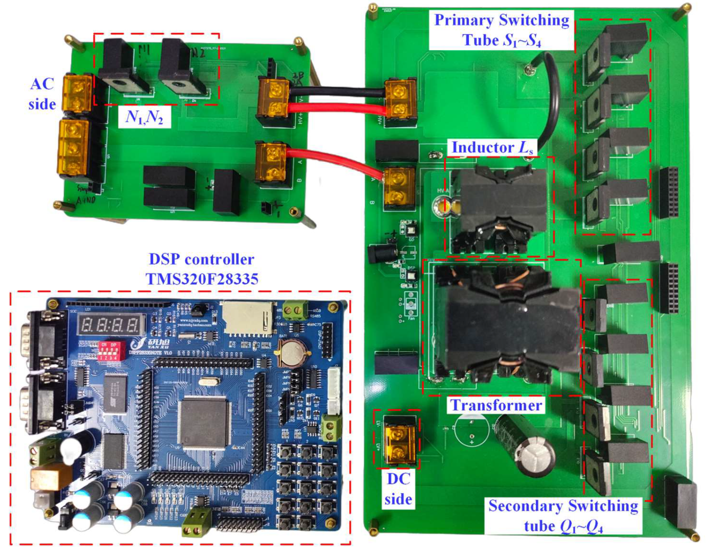
In the above work, the step-by-step constraints on the transformer ratios N and Ls are applied to gradually narrow their design ranges with the design requirements of the converter’s parameters, and the parameter optimization results of the transformer ratio N = 0.9 and Ls = 63 μH are finally determined by loss analysis. Therefore, in this section, a single-stage totem pole DAB AC-DC converter experimental prototype is built, as shown in Figure 14. Customized with three different groups of parameters of N and Ls, the experimental results under different parameter groups are compared to prove the effectiveness of the parameter optimization design method.
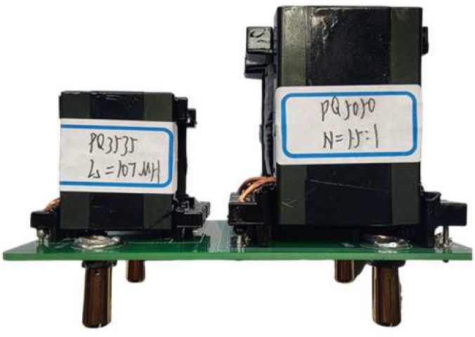
The transformer and power inductance for three groups of parameters are shown in Table 2. The first group of parameters is the optimized design result: N = 0.9, Ls = 65 μH; the second group of parameters is: N = 1, Ls = 55 μH, and the third group of parameters is: N = 1.5, Ls = 107 μH.
Figure 15 shows the experimental waveforms of the converter at operating condition (360 V, 800 W) with three groups of parameters. Among them, Figure 15a shows the experimental waveforms under the parameter combination of “N = 0.9, Ls = 65 μH” where the AC current amplitude Ig = 11.05 A; Figure 15b shows the experimental waveforms under the parameter combination of “N = 1, Ls = 55 μH”, where the AC current amplitude Ig = 11.14 A; Figure 15c shows the experimental waveform with parameter combination of “N = 1.5, Ls = 107 μH”, and the AC current amplitude Ig = 11.32 A. Through the test, the efficiencies of the converter in the three groups of parameters are 93.5%, 93.2%, and 91.2%, respectively.
Figure 16 shows the experimental waveforms of the converter at operating condition (400 V, 800 W) with three groups of parameters. Among them, Figure 16a shows the experimental waveforms under the parameter combination of “N = 0.9, Ls = 65 μH” where the AC current amplitude Ig = 11.15 A; Figure 16b shows the experimental waveforms under the parameter combination of “N = 1, Ls = 55 μH”, where the AC current amplitude Ig = 11.21 A; Figure 16c shows the experimental waveform with parameter combination of “N = 1.5, Ls = 107 μH”, and the AC current amplitude Ig = 11.4 A. Through the test, the efficiencies of the converter in the three groups of parameters are 92.5%, 92.1%, and 90.5%, respectively.
The efficiencies of each power under the three groups of parameters were tested separately, and the results are shown in Figure 17. When the output voltage Vs = 360 V, the overall efficiency of the converter under the first group of parameters is the highest and the peak efficiency reaches 93.7%. When the output voltage Vs = 400 V, the overall efficiency of the converter under the first group of parameters is the highest and the peak efficiency reaches 92.8%. According to the comparison of the experimental results in Figure 17a,b, the overall efficiency of the converter at the output voltage Vs = 360 V is higher than that at Vs = 400 V, which is consistent with the loss analysis results.
The above experimental results demonstrate the improvement of the converter’s overall efficiency under the parameters N = 0.9 and Ls = 65 μH. Compared with the efficiency of the converter under the remaining two groups of parameters, the overall efficiency of the parameter-optimized converter is improved by 0.7% and 1.9% at the output voltage Vs = 360 V and by 1% and 2.1% at Vs = 400 V, respectively.
However, as shown in Figure 18, there is an error between the computational and experimental efficiency of the designed parameters.
After comparison, it can be found that there are some deviations between the calculated and measured values of efficiency, with the largest deviation occurring at Vs = 360 V, P = 400 W, and at the parameters N = 1.5, Ls = 105 μH, the calculated value is 92.4% while the measured value is 90.5%, a difference of 1.9%.
This is mainly due to the following reasons: (1) the effect of temperature on resistance is not taken into account in the calculation of conduction loss; (2) the simplified model for calculating switching loss makes the switching loss inaccurate; (3) the Steinmetz equation taken in the calculation of core loss is not accurate enough for non-sinusoidal signal; (4) other converter losses besides the above mentioned losses are not taken into account. However, in general, the calculated and measured efficiency trends for the parameters are consistent.
7. Conclusions
To improve the overall efficiency of the single-stage DAB AC-DC converter, this paper proposes a parameter design method that considers multi-timescale analysis by combining the steady-state model in line cycle and switching cycle. Using the idea of step-by-step constraints establishes the safe design space and optimization design space of parameters. The design space of the parameters is reduced step by step, which reduces the computational amount of the loss analysis model. Compared with the traditional method based on the parameter design of the DAB DC-DC converter, the proposed optimization design method fully considers the steady-state characteristics of the line cycle of the DAB AC-DC converter, and the step-by-step constraint greatly accelerates the parameter design process. The final experimental results verify the effectiveness of the proposed parameter optimization design method.
Author Contributions
Conceptualization, C.Y.; methodology, Q.L.; validation, C.Y.; formal analysis, C.Y.; investigation, C.Y.; writing—original draft preparation, C.Y.; writing—review and editing, C.Y.; supervision, C.Y.; project administration, Q.L. All authors have read and agreed to the published version of the manuscript.
Funding
This research was supported by the Chongqing Municipal Technology Innovation and Application Development Special Key Project, grant No. CSTB2023TIAD-KPX0083.
Data Availability Statement
Data are contained within the article.
Conflicts of Interest
The authors declare no conflicts of interest.
Appendix A
The loss analysis of the DAB AC-DC converter is mainly composed of the following three parts: conduction losses, switching losses and core losses, which are derived as follows.
- (1)
- Conduction losses
The conduction loss Pcon of the converter mainly consists of the conduction loss of the switch Pcon_sw and the copper loss of the magnetic element Pcu.
The conduction loss of the switch Pcon_sw is:
The copper loss of the magnetic element Pcu is:
where Rds_on is the on-resistance of the switch, RLg is the winding resistance of the AC side inductor Lg, RLs is the winding resistance of the power inductor Ls, RTp, and RTs are the winding resistances of the primary and secondary sides of the high-frequency transformer, respectively.
- (2)
- Switching losses
The turn-on loss and turn-off loss of the converter are calculated as follows:
where fs denotes the switching frequency, ttr represents the turn-on and turn-off durations of the switch. And the energy stored in the switch’s capacitance Coss can be obtained by fitting the Coss-Vds curve from the datasheet of SCT3060AL.
- (3)
- Core losses
The magnitude of core loss is mainly related to the flux density Bm, magnetization frequency fs, material coefficients α and β, and core volume Vcore. The core loss is generally calculated using the Steinmetz equation (SE):
Specific design of transformers and inductors as follows:
For a high-frequency transformer with core model PQ5050, the AP calculation equation is:
where Ae is the core effective cross-sectional area and Aw is the core window area. PT is the transformer power, which is the sum of the transformer primary and secondary power. k0 is the core window utilization taken, J is the current density, Bm is the maximum flux density.
For the power inductor Ls with core model PQ3535, the AP calculation equation is:
where Ls is the inductance value and Ipeak is the peak inductance current.
References
- Everts, J.; Krismer, F.; Van den Keybus, J.; Driesen, J.; Kolar, J.W. Optimal ZVS modulation of single-phase single-stage bidirectional DAB ac–dc converters. IEEE Trans. Power Electron. 2014, 29, 3954–3970. [Google Scholar] [CrossRef]
- Zengin, S.; Boztepe, M. A novel current modulation method to eliminate low-frequency harmonics in single-stage dual active bridge AC–DC converter. IEEE Trans. Ind. Electron. 2020, 67, 1048–1058. [Google Scholar] [CrossRef]
- Jauch, F.; Biela, J. Combined phase-shift and frequency modulation of a dual-active-bridge AC–DC converter with PFC. IEEE Trans. Power Electron. 2016, 31, 8387–8397. [Google Scholar] [CrossRef]
- Sun, X.; Wang, H.; Qi, L.; Liu, F. Research on single-stage highfrequency-link SST topology and its optimization control. IEEE Trans. Power Electron. 2020, 35, 8701–8711. [Google Scholar] [CrossRef]
- Everts, J. Design and Optimization of an Efficient (96.1%) and Compact (2 kW/dm3) Bidirectional Isolated Single-Phase Dual Active Bridge AC-DC Converter. Energies 2016, 9, 799. [Google Scholar] [CrossRef]
- Yilmaz, M.; Krein, P.T. Review of Battery Charger Topologies, Charging Power Levels, and Infrastructure for Plug in Electric and Hybrid Vehicles. IEEE Trans. Power Electron. 2013, 28, 2151–2169. [Google Scholar] [CrossRef]
- Belkamel, H.; Kim, H.; Choi, S. Interleaved Totem-Pole ZVS Converter Operating in CCM for Single-Stage Bidirectional AC–DC Conversion with High-Frequency Isolation. IEEE Trans. Power Electron. 2021, 36, 3486–3495. [Google Scholar] [CrossRef]
- Weise, N.D.; Castelino, G.; Basu, K.; Mohan, N. A single-stage dualactive-bridge-based soft switched ac–dc converter with open-loop power factor correction and other advanced features. IEEE Trans. Power Electron. 2014, 29, 4007–4016. [Google Scholar] [CrossRef]
- Sha, D.; Zhang, D.; Zhang, J. A Single-Stage Dual-Active-Bridge AC–DC Converter Employing Mode Transition Based on Real-Time Calculation. IEEE Trans. Power Electron. 2021, 36, 10081–10088. [Google Scholar] [CrossRef]
- Li, X.; Wu, F.; Yang, G.; Liu, H. Improved Modulation Strategy for Single-Phase Isolated Quasi-Single-Stage AC–DC Converter to Improve Current Characteristics. IEEE Trans. Power Electron. 2020, 35, 4296–4308. [Google Scholar] [CrossRef]
- Li, J.; Yuan, L.; Gu, Q.; Sun, J.; Duan, R. A loss model-based efficiency optimization method for dual active-bridge DC-DC converters. J. Electrotechnol. 2017, 32, 66–76. [Google Scholar]
- Krismer, F. Modeling and optimization of bidirectional dual active bridge DC-DC converter topologies. Ph.D. Thesis, Zurich Federal Institute of Technology, Zurich, Switzerland, 2010. [Google Scholar]
- Biao, Z.; Qiang, S. Theory and Application Techniques of Dual Active Full-Bridge DC-DC Converters; Science Press: Beijing, China, 2017; pp. 7–10. [Google Scholar]
- Das, D.; Basu, K. Optimal design of a dual-active-bridge DC-DC converter. IEEE Trans Ind Electron 2021, 68, 12034–12045. [Google Scholar] [CrossRef]
- Wang, S.; Zheng, Z.; Li, Y. Optimal Design Methodology of Bidirectional Dual Active Bridge Series Resonant DC/DC Converter. In Proceedings of the 2019 IEEE 13th International Conference on Power Electronics and Drive Systems (PEDS), Toulouse, France, 9–12 July 2019; pp. 1–5. [Google Scholar]
- Zhang, Y.; Yang, G.; Li, J.; Kong, Z.; Zhu, X. A Modulation Scheme with Full Range ZVS and Natural Power Factor Correction for Bridgeless Single-Stage Isolated AC–DC Converter. IEEE Trans. Power Electron. 2023, 38, 195–205. [Google Scholar] [CrossRef]
- Biao, Z.; Song, Q.; Liu, W.; Liu, G.; Zhao, Y. Universal High-Frequency-Link Characterization and Practical Fundamental-Optimal Strategy for Dual-Active-Bridge DC-DC Converter Under PWM Plus Phase-Shift Control. IEEE Trans. Power Electron. 2015, 30, 6488–6494. [Google Scholar]
- Christopher, H.; Karoline, V.; Sebastian, Z.; Uwe, S.D. Electric vehicle route planning using real-world charging infrastructure in Germany. eTransportation 2021, 10, 100143. [Google Scholar]
- Mou, D.; Luo, Q.; Wei, Y.; Li, J.; Hou, N.; Long, T.; Li, Y. A periodic-steady-state analysis model in time-domain for dual active bridge converter. IEEE Trans Power Electron 2022, 37, 4121–4132. [Google Scholar] [CrossRef]
- Mallik, A.; Khaligh, A. Maximum Efficiency Tracking of an Integrated Two-Staged AC–DC Converter Using Variable DC-Link Voltage. IEEE Trans. Ind. Electron. 2018, 65, 8408–8421. [Google Scholar] [CrossRef]
- Steinmetz, C.P. On the law of hysteresis. AIEE Trans. 1892, 9, 3–64, Reprinted in Proc. IEEE 1984, 72, 196–221. [Google Scholar] [CrossRef]
Figure 1.
Totem pole DAB AC-DC converter topology.
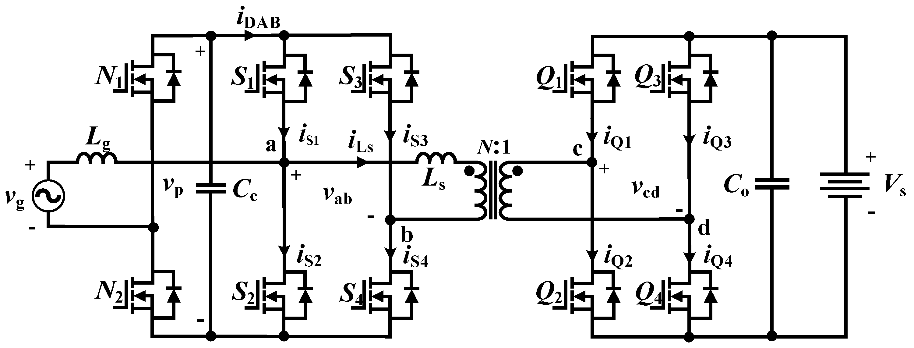
Figure 2.
Steady-state waveforms of the converter under EPS at Tg and Ts.

Figure 3.
Steady-state waveforms of switching cycle in Tg/2 under the condition (400 V, 800 W): (a) the peak-to-peak inductor current Ipp; (b) the inductor current RMS IL_RMS.
Figure 3.
Steady-state waveforms of switching cycle in Tg/2 under the condition (400 V, 800 W): (a) the peak-to-peak inductor current Ipp; (b) the inductor current RMS IL_RMS.

Figure 4.
Current of each switching under the condition (400 V, 800 W) when N = 1, Ls = 50 μH: (a) Primary Switch S1~S4; (b) Secondary Switch Q1~Q4.
Figure 4.
Current of each switching under the condition (400 V, 800 W) when N = 1, Ls = 50 μH: (a) Primary Switch S1~S4; (b) Secondary Switch Q1~Q4.

Figure 5.
Range of values of N and Ls under transmission power constraint.
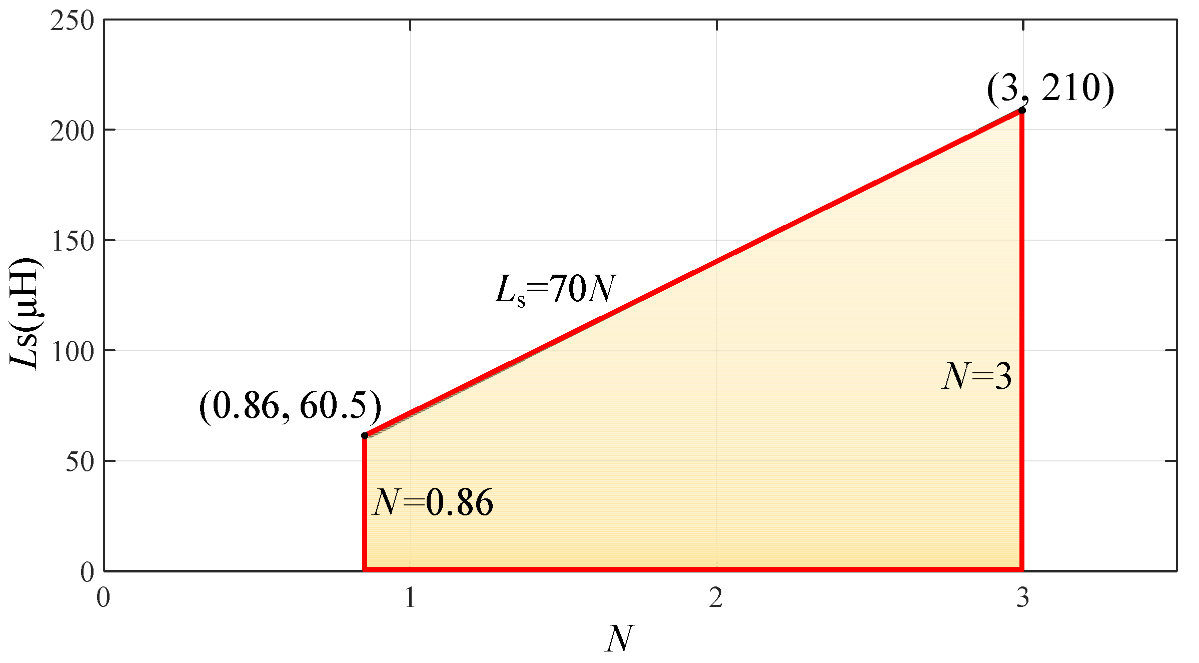
Figure 6.
Ipp at full load range when N = 1.5, Ls = 40 μH.

Figure 7.
Ipp distribution for all combinations of N and Ls at conditions (400 V, 800 W): (a) Ipp distribution for all N and Ls; (b) The region of parameters N and Ls satisfy the constraint.
Figure 7.
Ipp distribution for all combinations of N and Ls at conditions (400 V, 800 W): (a) Ipp distribution for all N and Ls; (b) The region of parameters N and Ls satisfy the constraint.

Figure 8.
Safe design space for parameters N and Ls.
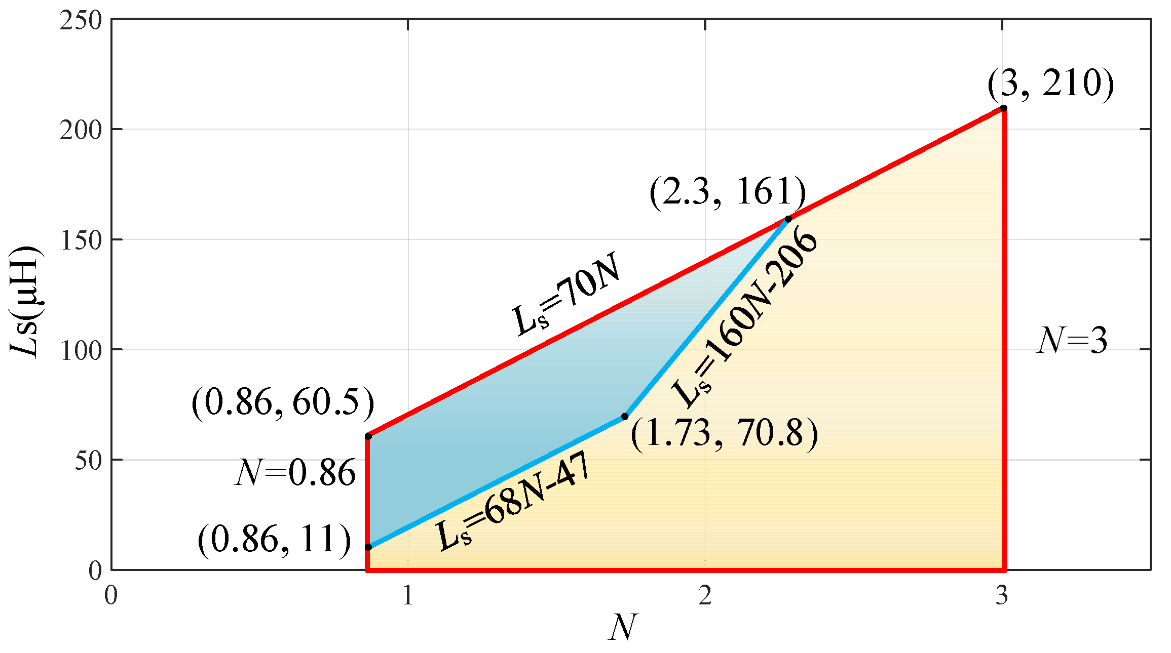
Figure 9.
Variation of IRMS with different combinations of parameters N and Ls under the condition (400 V, 800 W): (a) IRMS-Ls curve at N = 1.5; (b) IRMS-Ls curve at different N.
Figure 9.
Variation of IRMS with different combinations of parameters N and Ls under the condition (400 V, 800 W): (a) IRMS-Ls curve at N = 1.5; (b) IRMS-Ls curve at different N.
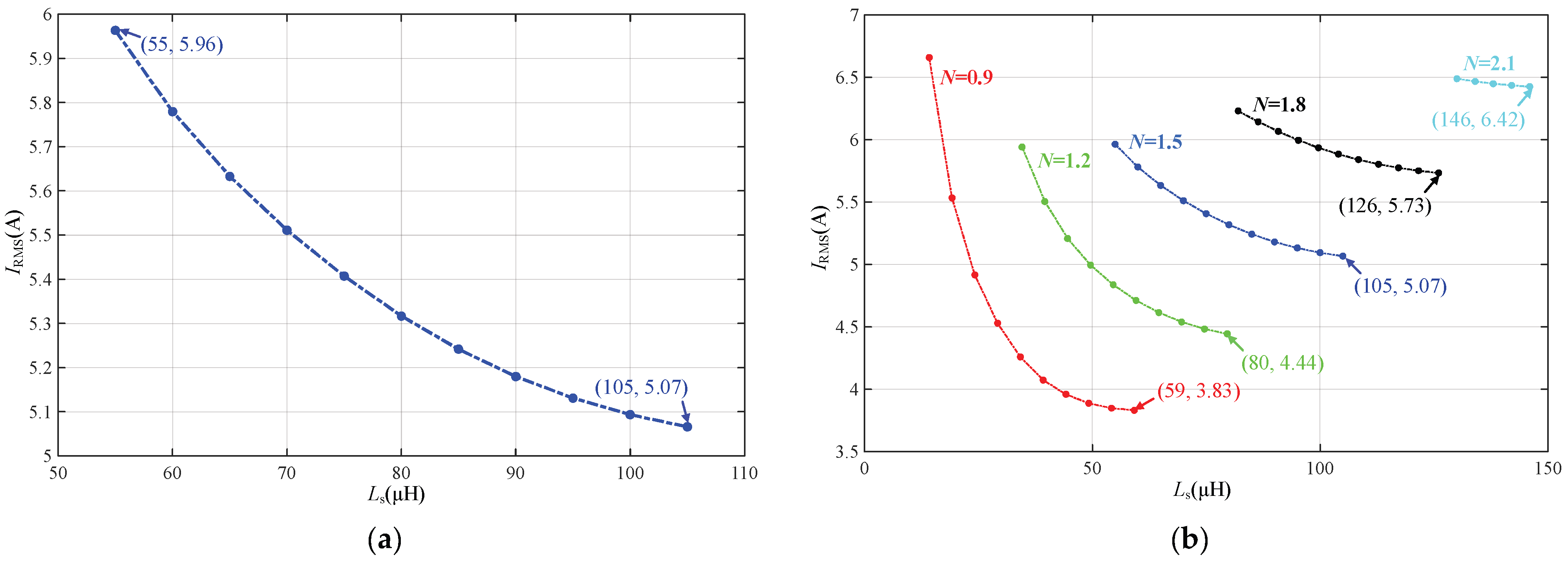
Figure 10.
ZVS realizations with different parameters N and Ls under the condition (400 V, 800 W): (a) The number of hard-switching under Tg/2 at N = 1.5; (b) The number of hard-switching under Tg/2 at different N.
Figure 10.
ZVS realizations with different parameters N and Ls under the condition (400 V, 800 W): (a) The number of hard-switching under Tg/2 at N = 1.5; (b) The number of hard-switching under Tg/2 at different N.
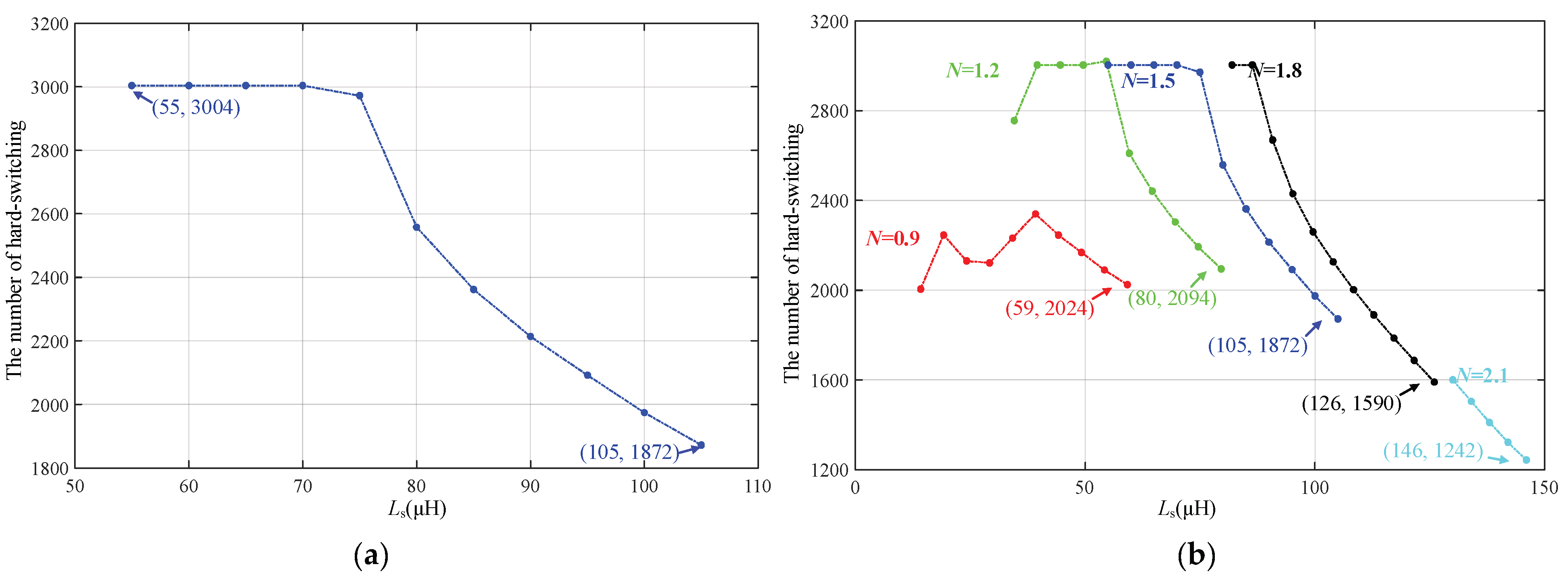
Figure 11.
Optimization design space for parameters N and Ls.
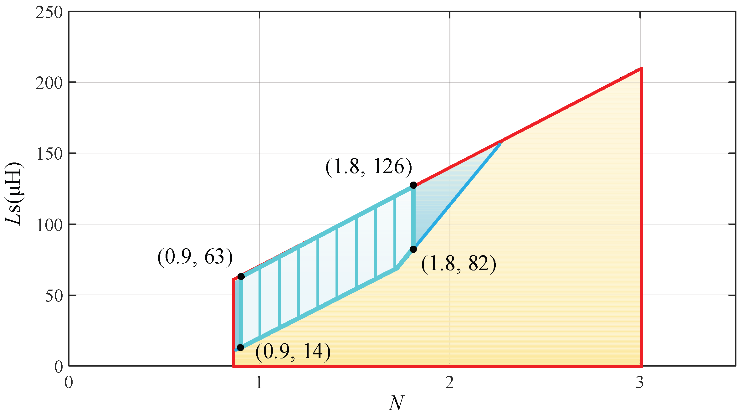
Figure 12.
Discrete Statistics of IRMS and ZVS for different parameters N and Ls.

Figure 13.
Power losses at different working conditions for different parameters: (a) output voltage Vs = 360 V; (b) output voltage Vs = 400 V.
Figure 13.
Power losses at different working conditions for different parameters: (a) output voltage Vs = 360 V; (b) output voltage Vs = 400 V.
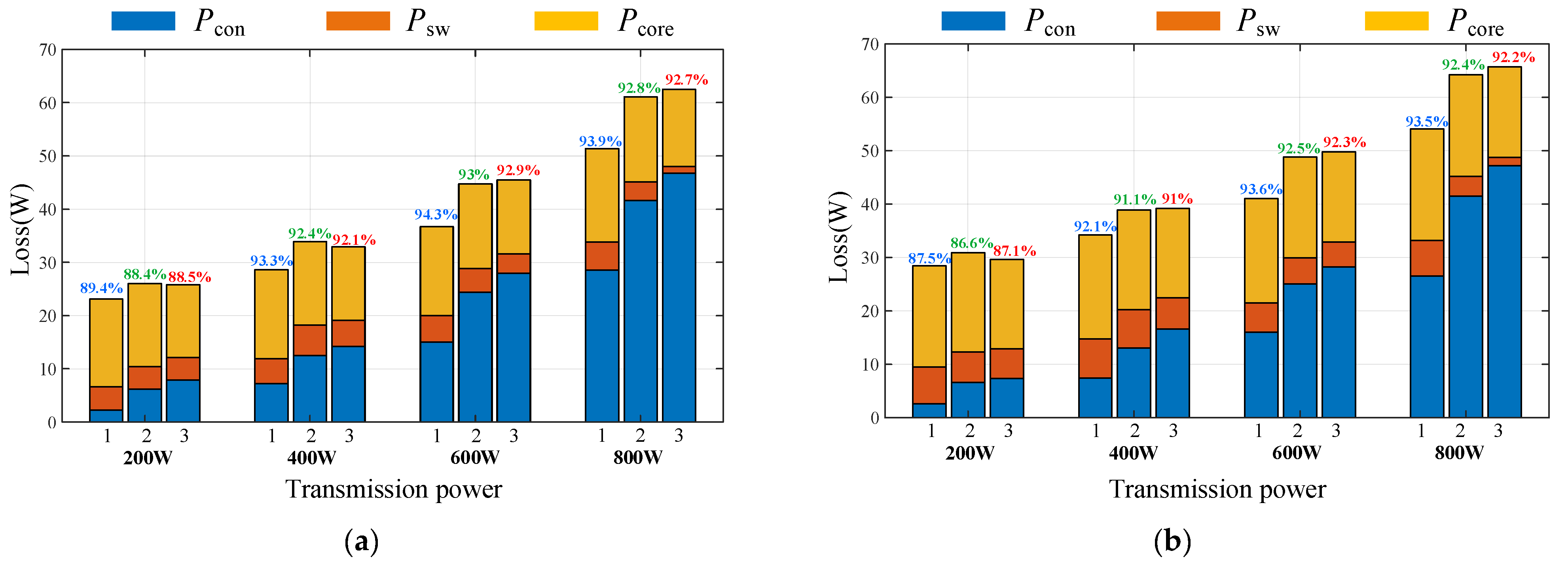
Figure 14.
Single-stage totem pole DAB AC-DC experimental prototype.

Figure 15.
Waveforms of each group of parameters under condition (360 V, 800 W): (a) N = 0.9, Ls = 65 μH; (b) N = 1, Ls = 55 μH; (c) N = 1.5, Ls = 107 μH.
Figure 15.
Waveforms of each group of parameters under condition (360 V, 800 W): (a) N = 0.9, Ls = 65 μH; (b) N = 1, Ls = 55 μH; (c) N = 1.5, Ls = 107 μH.
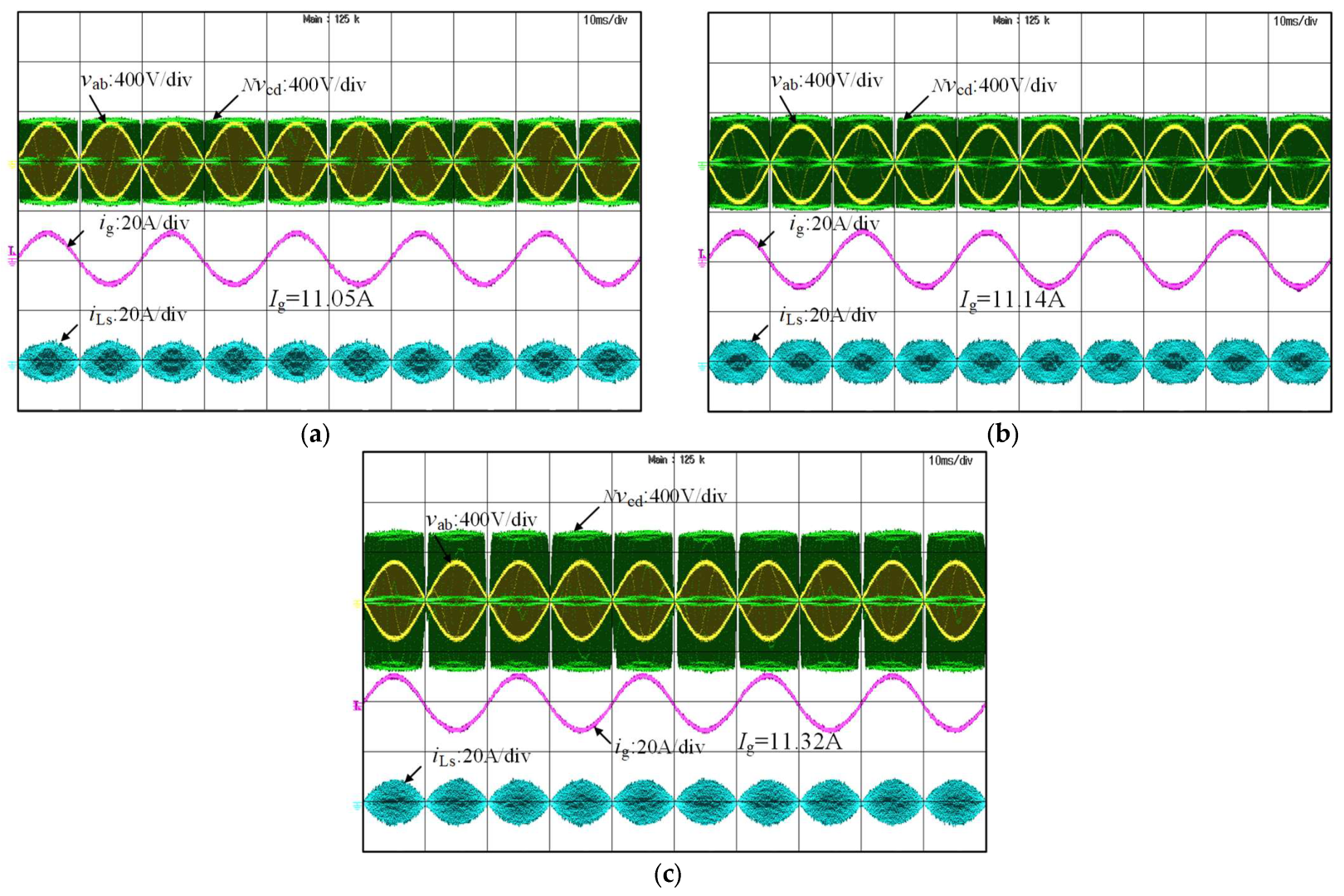
Figure 16.
Waveforms of each group of parameters under condition (400 V, 800 W): (a) N = 0.9, Ls = 65 μH; (b) N = 1, Ls = 55 μH; (c) N = 1.5, Ls = 107 μH.
Figure 16.
Waveforms of each group of parameters under condition (400 V, 800 W): (a) N = 0.9, Ls = 65 μH; (b) N = 1, Ls = 55 μH; (c) N = 1.5, Ls = 107 μH.

Figure 17.
Efficiency curves of three groups of parameters under different operating conditions: (a) Vs = 360 V; (b) Vs = 400 V.
Figure 17.
Efficiency curves of three groups of parameters under different operating conditions: (a) Vs = 360 V; (b) Vs = 400 V.

Figure 18.
Comparison of the calculated efficiency with the measured efficiency: (a) Vs = 360 V; (b) Vs = 400 V.
Figure 18.
Comparison of the calculated efficiency with the measured efficiency: (a) Vs = 360 V; (b) Vs = 400 V.


Table 1.
DAB AC-DC converter design indicators.
| Parameter | Value | Parameter | Value |
|---|---|---|---|
| Input Voltage vg | 110 Vrms | Output voltage Vs | 360~400 V |
| Line frequency fg | 50 Hz | Switching frequency fs | 100 kHz |
| Rated power PN | 800 W | MOSFET | SCT3060AL |
Table 2.
The transformers and inductor with different parameters.
| Group I | Group II | Group III |
|---|---|---|
| N = 0.9:1 Ls = 65 μH | N = 1:1 Ls = 55 μH | N = 1.5:1 Ls = 107 μH |
 |  |  |
Disclaimer/Publisher’s Note: The statements, opinions and data contained in all publications are solely those of the individual author(s) and contributor(s) and not of MDPI and/or the editor(s). MDPI and/or the editor(s) disclaim responsibility for any injury to people or property resulting from any ideas, methods, instructions or products referred to in the content. |
© 2024 by the authors. Licensee MDPI, Basel, Switzerland. This article is an open access article distributed under the terms and conditions of the Creative Commons Attribution (CC BY) license (https://creativecommons.org/licenses/by/4.0/).
Share and Cite
MDPI and ACS Style
Yu, C.; Luo, Q. A Parameter Optimization Design Method for Single-Phase Dual Active Bridge AC-DC Converter. Energies 2024, 17, 1955. https://doi.org/10.3390/en17081955
AMA Style
Yu C, Luo Q. A Parameter Optimization Design Method for Single-Phase Dual Active Bridge AC-DC Converter. Energies. 2024; 17(8):1955. https://doi.org/10.3390/en17081955
Chicago/Turabian StyleYu, Chengyang, and Quanming Luo. 2024. "A Parameter Optimization Design Method for Single-Phase Dual Active Bridge AC-DC Converter" Energies 17, no. 8: 1955. https://doi.org/10.3390/en17081955
Note that from the first issue of 2016, this journal uses article numbers instead of page numbers. See further details here.