
Design of Broadband Doherty Power Amplifier Based on Misaligned Current Phase

1
Space Star Technology Co., Ltd., Beijing 100086, China
2
School of Electronic Information Engineering, Yangtze Normal University, Chongqing 408102, China
3
School of Microelectronics and Communication Engineering, Chongqing University, Chongqing 400044, China
*
Author to whom correspondence should be addressed.
Energies 2024, 17(9), 2006; https://doi.org/10.3390/en17092006
Submission received: 27 March 2024
/
Revised: 18 April 2024
/
Accepted: 22 April 2024
/
Published: 24 April 2024
(This article belongs to the Section F3: Power Electronics)
Abstract
:A broadband Doherty power amplifier (DPA) always experiences an efficiency degradation between two efficiency peaks, especially at two side bands. In this study, the efficiency degradation was demonstrated to be caused caused by the in-phase power combining at the saturation power level. To solve this problem, current misalignment was introduced into the broadband DPA design. The carrier and peaking PA have different current phases when performing the power combination at the saturation power level. In this work, it was also demonstrated that the efficiency in the high-power region of a DPA can be improved by elaborately using misaligned current phases. A detailed analysis and the design procedure of a broadband DPA are presented in this paper. And a 1.5–2.45 GHz broadband DPA was implemented and measured. The fabricated DPA achieves a saturation output power of 42.7–44.9 dBm, a saturation drain efficiency (DE) of 62.7–74.1% and a gain of 10.2–13.9 dB over 1.5–2.45 GHz. Moreover, the fabricated DPA also achieves a 6 dB back-off DE of more than 49.1% in the frequency band of interest.
1. Introduction
Wireless communication is moving from the fifth generation (5G) to the six generation (6G). The whole industry chain is accelerating beyond imagination [1]. Everyone and everything will be connected to the 6G network [1]. It is inevitable that every smart device will need to emit signals in the Internet of Things (IoT) era, leading to an unprecedented demand on power amplifiers (PAs) [2]. In addition to spatial multiplexing (multi-input, multi-output), complex signal modulation and wideband techniques are very important for increasing the communication data rate. Meanwhile, enhancing the efficiency of PAs has always been a design goal [3,4]. In line with the above factors, PAs are expected to have a high back-off efficiency over a wide bandwidth. Recently, a Doherty power amplifier (DPA) demonstrated its unparalleled advantages due to its simple structure [5,6,7,8,9].
A DPA can maintain high efficiency over a certain output back-off (OBO) power range. However, it is considered that the DPA has a narrow bandwidth. It has been validated in [9] that the impedance inverter in the DPA combiner limits the operation bandwidth. Actually, the higher the impedance inversion ratio of the impedance inverter, the narrower the bandwidth that the DPA achieves. Therefore, some works have extended the working bandwidths of DPAs using a modified combined network with a reduced impedance inversion ratio [10,11,12,13,14,15,16]. A 0.55–1.1 GHz broadband DPA was realized in [14] using a modified impedance inverter. And in [16], a modified load modulation combiner was proposed to extend the bandwidth of an asymmetrical DPA. A 1.4–2.5 GHz DPA was implemented in [16], achieving a saturation and a 9 dB back-off drain efficiency (DE) of 61–75.5% and 44.6–54.6%, respectively.
In addition to the impedance inverter, high-order output matching networks (OMNs) in a DPA also limit its bandwidth [17]. This is because a high-order network leads to a more drastic phase variation compared to the frequency. For removing high-order OMNs, a post-matching Doherty architecture was proposed in [17]. In a post-matching DPA, the OMNs of the carrier and peaking amplifiers are placed behind the combing point, creating a high-order post-matching network. And the impedance inverter is replaced by a low order network [18]. In this way, the post-matching Doherty architecture can be considered a promising method for extending the bandwidth of DPAs [19,20,21,22,23]. The authors in [23] designed a post-matching DPA covering 1.7–2.8 GHz. This DPA maintains a DE of more than 50% over an OBO power range of 6 dB.
For high-efficiency DPAs, the back-off DE is more important than the saturation counterpart [6]. To further improve the back-off DE and extend the bandwidth of the DPA, a continuous-mode DPA (CM-DPA) was developed and analyzed [24,25,26,27,28,29]. The CM-DPA could achieve a high DE and wide bandwidth simultaneously based on the continuous-mode PA theories [24,25]. In [25], a broadband CM-DPA covering 1.5–2.6 GHz (relative bandwidth of 53%) was implemented, maintaining a DE of 41.3–55.1% over a 6 dB OBO power range.
Furthermore, the bandwidth of the DPA can also be extended using novel design methods [30,31,32,33]. In [30], an ultra-wideband DPA based on a closed-form design method was presented. A comprehensive analysis was conducted in [30] to describe the design of the ultra-wideband DPA. In [33], complex combining impedance and non-infinity peaking impedance were introduced into the DPA design, leading to an extension of the operation bandwidth.
Though the bandwidth of a DPA can be extended through so many advanced design methods, efficiency degradation can always be observed in the high-power region. There are some innovative works that have been conducted to address this problem [34,35,36]. In [34], an adaptive technique was adopted in the carrier and peaking PAs to dynamically tune the gate voltage, enhancing the efficiency of the DPA. In [35], a digitally assisted technique was used to control the phase offset angles between carrier and peaking PAs, leading to an improved efficiency throughout the back-off region. Notice that the two methods above need additional analog circuits or digital algorithms. This will increase the circuit complexity.
Unlike the methods in [34,35], a novel design method without any additional assistant circuits and algorithms was proposed in [36] to enhance the efficiency of the DPA over the OBO range. In [36], a complex-valued combining load impedance was introduced into the DPA design. After a comprehensive analysis, a complex-valued combining impedance was carefully selected to construct a 1.35–1.7 GHz DPA. This DPA maintains a DE of >50% over a 9 dB OBO power range. Notice that a specific complex-valued combining impedance is required by the DPA at each operation frequency point. This may limit the bandwidth of the DPA.
Different from the efficiency enhancement techniques in [34,35,36], a misaligned current phase was introduced into the broadband DPA design to compensate for the efficiency degradation. The proposed method does not need any additional assistant circuits or algorithms. Moreover, it has no effect on the operation bandwidth of the DPA. The misalignment current phase was realized using different matching networks for the carrier and peaking PAs. In this way, the carrier and peaking PAs have different saturation current phases versus frequency at the combining point. And the efficiency of the DPA can be enhanced over the OBO power range.
In this paper, a theoretical explanation of the efficiency degradation of the broadband DPA will be presented in Section 2. As described in this section, the misaligned current phase was introduced into a broadband DPA. Section 3 discusses the design and simulation of a broadband DPA with a misaligned current phase. The experimental results of the fabricated DPA will be given in Section 4.
2. Theoretical Analysis
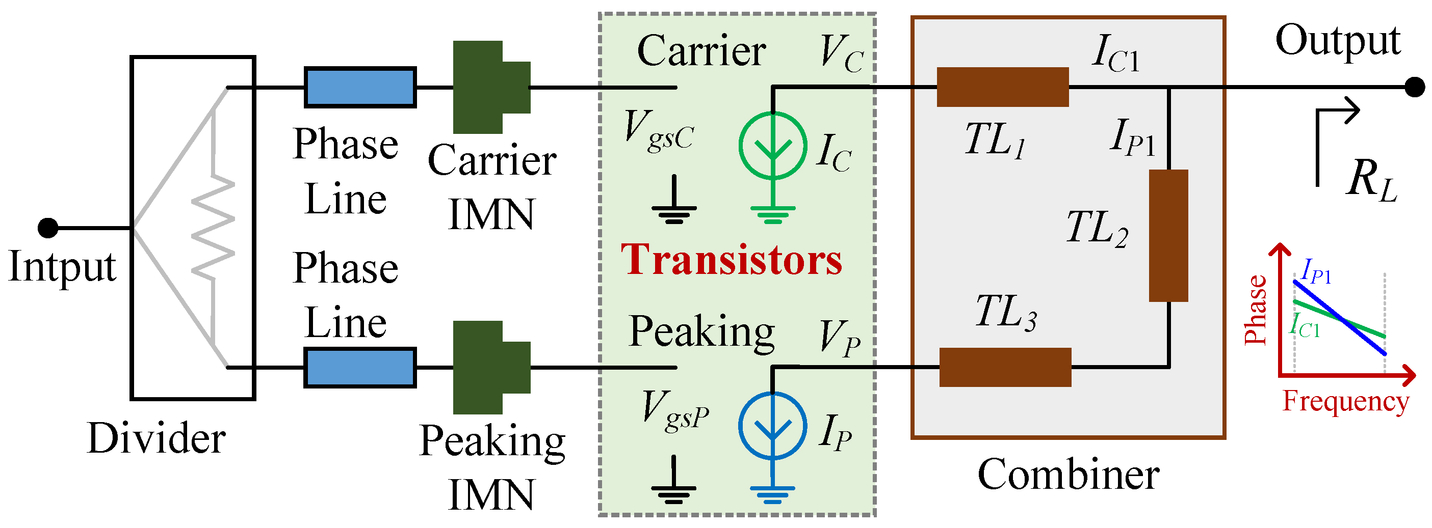
The proposed DPA consists of carrier and peaking transistors together with their input matching networks (IMNs). And a combiner is used to combine the output power from the carrier and peaking transistors, as well as realize active load modulation, as shown in Figure 1. The DPA is loaded with an impedance . Notice that a post-matching network is needed if is not equal to 50 . For simplicity, it is assumed in this paper that the DPA is symmetrical. This means that the carrier and peaking transistors are the same. To enhance the DE of the DPA in the back-off power range, a misaligned current phase was introduced into the DPA design in this study, as shown in Figure 1. This current misalignment was realized through carefully designing the IMNs and tuning the phase compensation line before the carrier PA or the peaking PA.
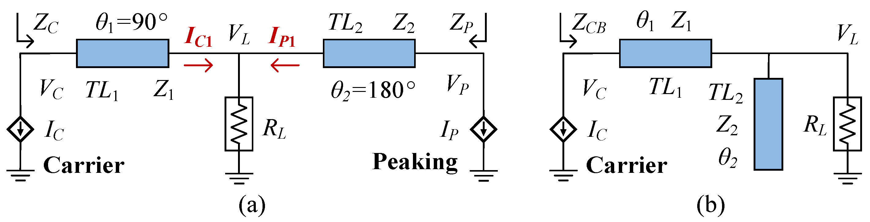
According to the theoretical analysis in [29], the most favorable Doherty combiner can be simplified as in Figure 2a. In this figure, the carrier and peaking transistors are represented by current generators and , respectively. The combiner is composed of two transmission lines TL1 and TL2, as shown in Figure 2a. The electronic lengths of TL1 and TL2 should be = 90° and = 180° at the center working frequency . Moreover, the characteristic impedance of TL1 and TL2 should be = = , where is the optimal impedance of the utilized transistor. Meanwhile, the combining load is = .
2.1. Load Modulation at Low Power Region
At the low-power region, the peaking transistor is in the off state. Here, the structure of the DPA is depicted in Figure 2b. Now, the cascaded network that is composed of TL1 and TL2 has an -matrix
where , , and are as follows:
In the above equations, f is the normalized frequency (normalized to the center frequency ).
In using (1)–(5), the fundamental load impedance of the carrier transistors at the low-power region can be obtained using
2.2. Drain Efficiency Analysis
The above analysis ignored the load modulation in the high-power region. The following parts will analyze the active load modulation of the carrier and peaking transistors in the high-power region.
For the high-power region, Figure 2a should be used to evaluate the active load modulation. In this situation, the -matrices of TL1, and TL2 can be expressed as follows:
Based on Equations (7)–(9), the -matrix of the Doherty combiner can be derived using
Through using (10), the fundamental drain voltages of the carrier and peaking transistors can be obtained using
In Equations (11) and (12), the currents of the carrier transistors ( in Figure 2) are related to the input voltage and can be expressed as
where is the trans-conductance of the transistor, and is the normalized input voltage. and are designated as = 1 and 0 1 in this paper. To ensure the in-phase power combining, a phase delay was introduced into . Normally, = 90° is used.
For the peaking transistor, its current is related to the input voltage and the switched-on time. To prevent the carrier PA from over-saturation in the low-power region, the peaking transistor should be switched on earlier when . Here, the real part of is defined as k, that is,
Then, the in Figure 2 can be expressed as
Equation (15) means that the peaking PA is switched on at .
Through using (11)–(15), the output power of the DPA is
and the DC power can be calculated using
where and are the DC currents that can be expressed as follows:
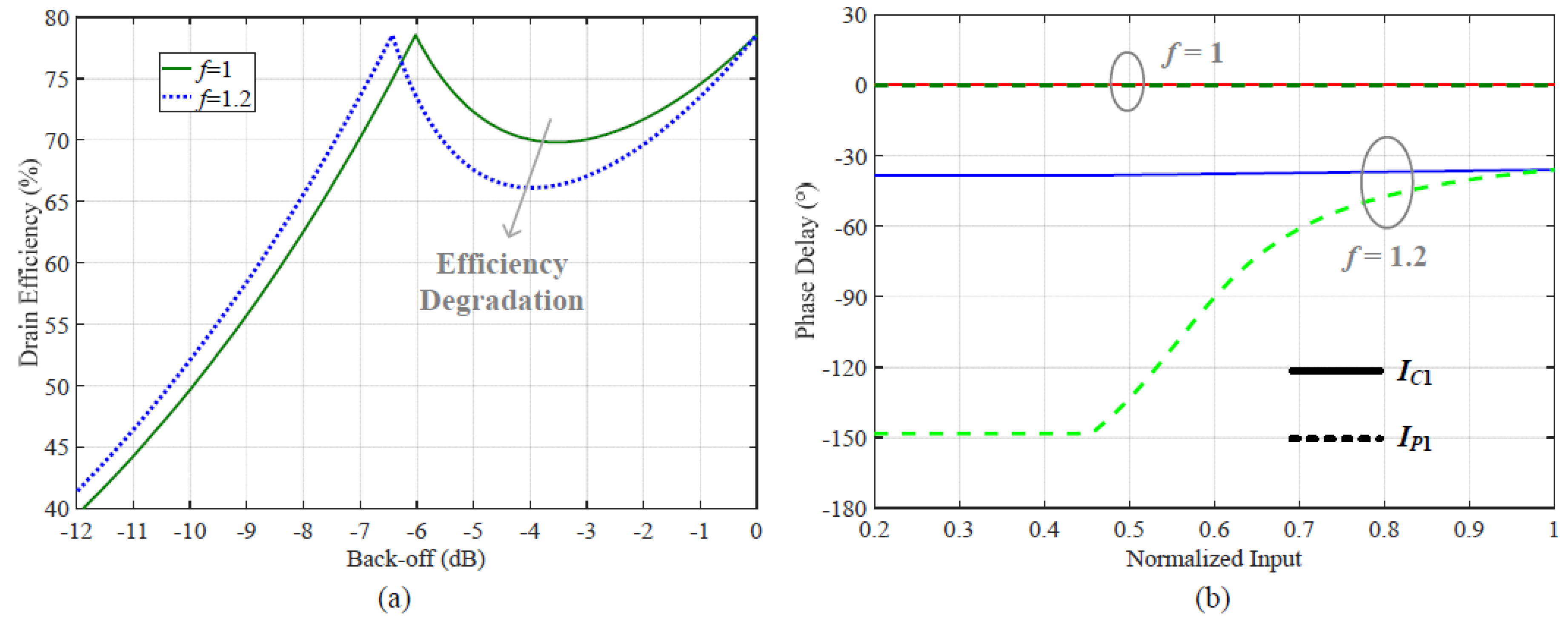
Through using (16)–(19), the DE of the DPA can be calculated using . Figure 3a depicts the DE of the DPA versus output back-off (OBO) power level when f = 1 and f = 1.2. In this figure, = 90° is utilized when calculating the DE. As stated in [29], the DE of the DPA at the OBO power level does not decreases along with f, deviating from the center frequency. Nevertheless, the lowest DE in the back-off power range becomes smaller and smaller as f deviates from f = 1. For example, compared to when f = 1, there is an efficiency degradation in the back-off power range when f = 1.2, as shown in Figure 3a.
Based on our analysis, the efficiency degradation is caused by a phase misalignment between the currents of the carrier and peaking PAs in the back-off range when f deviates from f = 1. Through using (7), (11) and (13), the current of the carrier PA at the combining point can be derived as
and through using (9), (12) and (15), the current of the peaking PA at the combining point can be derived as
Figure 3b depicts the phases of and versus normalized input when f = 1 and f = 1.2. In this figure, is set to 90°. In this situation, there is no phase difference between and at the saturation power level. However, a phase difference between and can be observed in the back-off power range when f deviates from f = 1, leading to a decrease in the DE, as shown in Figure 3.
For simplicity, the phase difference between and at the saturation power level is designated as :
where and are the phases of and at the saturation power level and can be derived using Equations (20) and (21).
From the above analysis, there will be a DE degradation in the OBO power range if is kept at zero over a wide bandwidth. To solve this problem, a misaligned current phase was introduced in this study. That is, a non-zero was used to enhance the DE of the DPA in the back-off power range when f deviates from f = 1. To validate the proposed theory, = 14.6° was introduced into the DPA when f = 1.2, as shown in Figure 4a. In this situation, the theoretical DE of the DPA when f = 1.2 is shown in Figure 4b. For comparison, the theoretical DE of the DPA with = 0° is also shown in Figure 4b. The figure indicates that the DE of the DPA was enhanced by introducing phase misalignment at the saturation power level.
3. Construction of a Broadband DPA
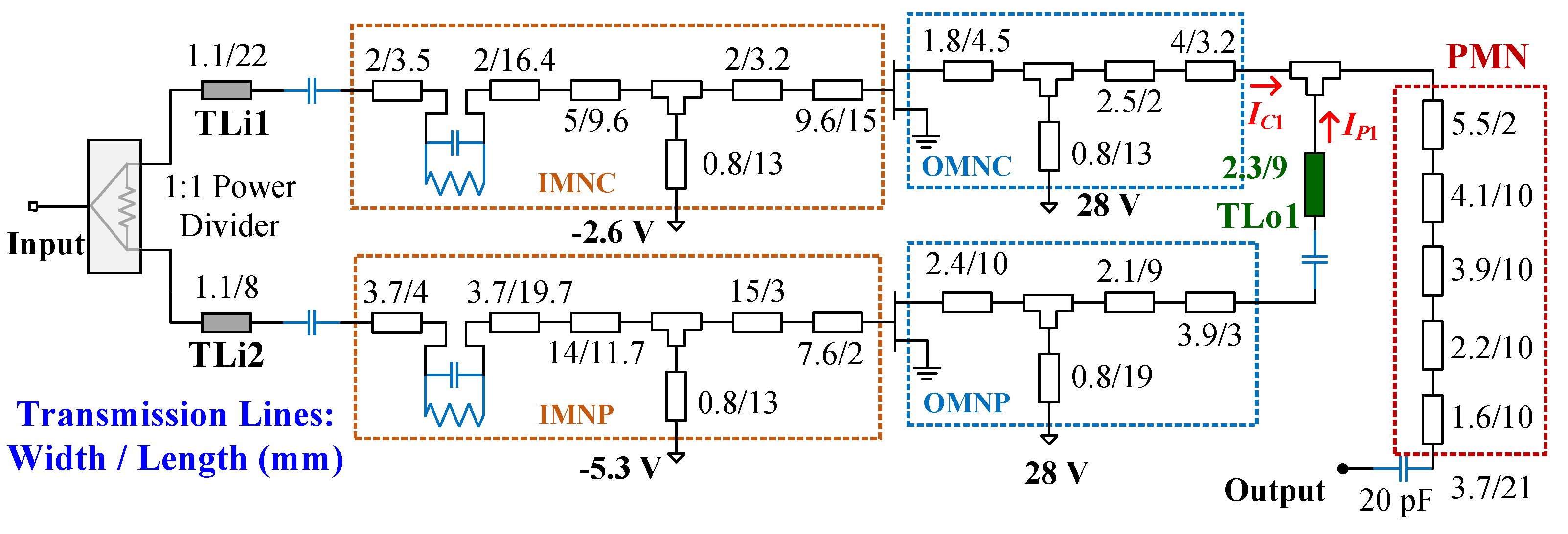
This part provide details on the design of a broadband DPA. Both the carrier and peaking transistors were CG2H40010F from Wolfspeed. The gate voltages of the carrier and peaking transistors were −2.9 V and −5.3 V, respectively. And the carrier and peaking transistors had the same drain voltage of 28 V. The optimal impedance of this kind of transistor was set to = 30 . And the combining load was set to /2 = 15 . Across the simulations, a Rogers 4350B substrate with a thickness of 20 mil was utilized. Considering the above analysis, the design bandwidth was set to 1.5–2.4 GHz. The design of the DPA was conducted in an Advanced Design System (ADS) simulator. And the whole schematic of the designed DPA is shown in Figure 5. The design steps of the DPA are similar to those in [29] and can be concluded to have been as follows.
Firstly, TL1 is replaced by a network, because the utilized transistor has intrinsic elements. In this design, TL1 consists of the intrinsic elements and an OMN of the carrier transistor (OMNC in Figure 5).
Secondly, TL2 is also replaced by a network, which consists of the intrinsic elements of the utilized transistor, the OMN of the peaking transistor (OMNP) and an impedance tuning line TLo1, as shown in Figure 5.
Thirdly, due to the combining load being = 15 , a PMN was designed to match a 50 standard load to .
Then, two IMNs (IMNC and IMNP in Figure 5) were constructed to, respectively, match the carrier and peaking transistors at the input terminals. The IMNs of the carrier and peaking transistors have the same structure. But the dimensions of the utilized transmission line are different, because different gate bias voltages were adopted.
Finally, A two-stage Wilkinson power divider was implemented to divide input power equally to the carrier and peaking paths. And two transmission lines TLi1 and TLi2 were inserted before the carrier and peaking PAs to tune the current phases of and .
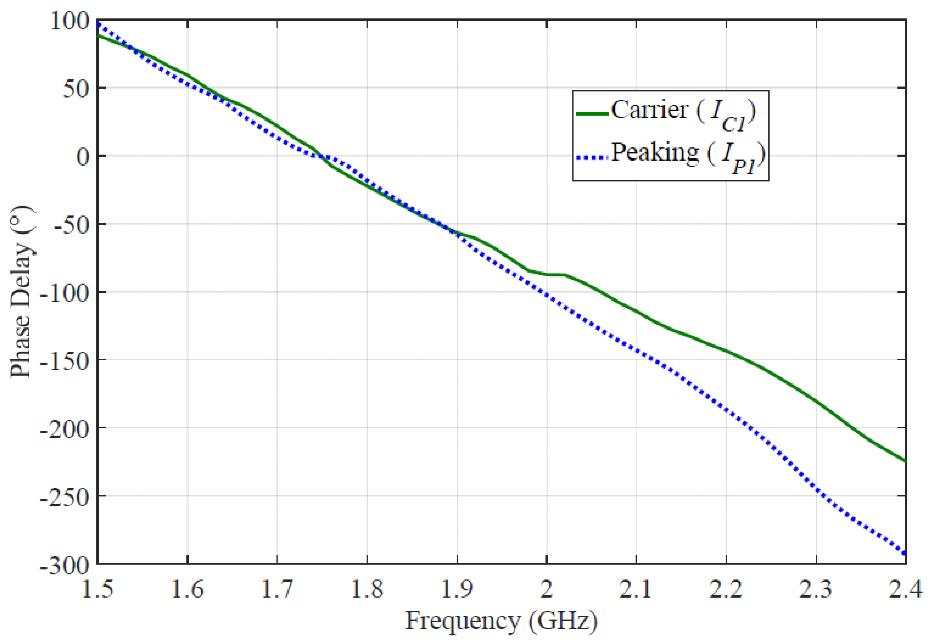
After implementing the DPA, the phases of the currents and were simulated based on Figure 5. The simulation results are shown in Figure 6. This figure indicates that a phase difference between and was obtained at the saturation power level over 2.0–2.4 GHz. This phase difference can be used to enhance the DE of the designed DPA in the OBO power range.
Furthermore, the DE and gain of the designed DPA were simulated across 1.5–2.4 GHz and with a step of 0.1 GHz. The simulation results are depicted in Figure 7a,b. Based on Figure 7, apparent Doherty behavior was achieved using the implemented DPA. The simulated DE was larger than 50% over an OBO power level of 6 dB. And the simulated gain was larger than 10 dB over 1.5–2.4 GHz.
4. Experimental Results
Photographs of the experimental environment of the fabricated DPA are shown in Figure 8. A signal generator, a spectrum analyzer, a driver, a DC supply and an attenuator were used to test the DPA. To automatically test the DPA, the above equipment were controlled using a computer via Matlab. When testing the DPA, the input power and operation frequency were measured. And the output power of the DPA was collected using the spectrum analyzer and then recorded using the PC. Meanwhile, the DC power was also recorded using the PC. In this way, the output power, DE and gain of the DPA could be automatically calculated and displayed on the PC.
Across the experiment, the gate voltage of the carrier PA was −2.8 V (the quiescent current was 40 mA), and the gate voltage of the peaking PA was −5.5 V. The drain voltages of the carrier and peaking transistors were 28 V.
Under a continuous wave (CW) signal excitation, the measured DEs and gains of the DPA with respect to the output power at some frequencies are illustrated in Figure 9. This figure indicates that no obvious DE degradation can be observed at 2.3 GHz and 2.45 GHz, while the maximum output power of the DPA was reduced at 2.45 GHz because of the misaligned current phase. From Figure 9, the fabricated DPA achieves a good DE performance over 1.5–2.45 GHz. Moreover, at the saturation power level, the measured gain was larger than 10 dB.
To clearly observe the measured results over the frequency band of interest, the measured saturation power and gain are illustrated in Figure 10. This figure indicates that the maximum output power of the fabricated DPA ranges from 42.7 to 44.9 dBm over 1.45–2.45 GHz. And the measured saturation gain of the fabricated DPA was 9.4–13.9 dB over 1.45–2.45 GHz.
The measured DEs of the fabricated DPA versus working frequency at the saturation and the 3 dB OBO and 6 dB OBO power levels are shown in Figure 11. The fabricated DPA achieves a DE of 62.7–74.1% at the maximum power level over 1.45–2.45 GHz. At the 3 dB OBO power level, the measured DE of the fabricated DPA ranges from 54.3 to 66.6% across 1.45–2.45 GHz. And at the 6 dB OBO power level, the fabricated DPA achieves a DE of 40.5–59.8% over 1.45–2.45 GHz. Notice that the 6 dB back-off DE is larger than 49% over 1.5–2.45 GHz, as shown in Figure 11.
5. Conclusions
In a broadband DPA, efficiency degradation can always be observed between two efficiency peaks when the operation frequency deviates from the center point. The reason that causes the efficiency degradation was analyzed in this paper. To address this problem, phase misalignment was introduced into the currents of the carrier and peaking PAs at the saturation power level. This means that the carrier and peaking PAs see different saturation current phases at the combining point. In this way, the efficiency of the DPA can be enhanced between two efficiency peaks. To achieve a misaligned saturation current phase between the carrier and peaking PAs, different matching typologies can be used. Moreover, novel phase compensation techniques, like in [37], can also be utilized to achieve a misaligned saturation current phase. Though the misaligned current phase has the potential to enhance the efficiency of a broadband DPA over the high-power range, the maximum output power of the broadband DPA will be affected. The proposed method was validated in this study through a theoretical analysis and a fabricated DPA. The fabricated DPA achieves a saturation output power of more than 42.7 dBm, a saturation DE of more than 63.4% and a 6 dB back-off DE of more than 49.1% over 1.5–2.45 GHz.
Author Contributions
Writing—original draft preparation, Y.H. and D.G.; writing—review and editing, D.G. and W.S.; supervision, W.S. All authors have read and agreed to the published version of the manuscript.
Funding
This research was funded in part by the Science and Technology Research Project of Chongqing Municipal Education Commission under grant number 010725111 and in part by the CAST funding program under grant number 2022LX-312-Y-GZ-15.
Data Availability Statement
The original contributions presented in the study are included in the article, further inquiries can be directed to the corresponding author.
Conflicts of Interest
Author Yinlong Hu was employed by the company Space Star Technology Co., Ltd. The remaining authors declare that the research was conducted in the absence of any commercial or financial relationships that could be construed as a potential conflict of interest.
References
- Chataut, R.; Nankya, M.; Akl, R. 6G Networks and the AI Revolution—Exploring Technologies, Applications, and Emerging Challenges. Sensors 2024, 24, 1888. [Google Scholar] [CrossRef] [PubMed]
- Carcangiu, S.; Fanni, A.; Montisci, A. A closed form selected mapping algorithm for PAPR reduction in OFDM multicarrier transmission. Energies 2022, 15, 1938. [Google Scholar] [CrossRef]
- Yang, K.; Yang, R.; Zhang, P.; Shi, W.; Hu, C.; Shi, W. Development review of highly efficient sequential power amplifier with extended back-off range for broadband application. Energies 2024, 17, 161. [Google Scholar] [CrossRef]
- Popovic, Z. Amping up the PA for 5G: Efficient GaN power amplifiers with dynamic supplies. IEEE Microw. Mag. 2017, 18, 137–149. [Google Scholar] [CrossRef]
- Nasri, A.; Estebsari, M.; Toofan, S.; Piacibello, A.; Pirola, M.; Camarchia, V.; Ramella, C. Design of a Wideband Doherty Power Amplifier with High Efficiency for 5G Application. Electronics 2021, 10, 873. [Google Scholar] [CrossRef]
- Ramella, C.; Piacibello, A.; Quaglia, R.; Camarchia, V.; Pirola, M. High Efficiency Power Amplifiers for Modern Mobile Communications: The Load-Modulation Approach. Electronics 2017, 6, 96. [Google Scholar] [CrossRef]
- Martin, D.N.; Barton, T.W. Inphasing signal component separation for an X-Band Outphasing power amplifier. IEEE Trans. Microw. Theory Tech. 2021, 69, 1661–1674. [Google Scholar] [CrossRef]
- Choi, H. A Doherty Power Amplifier for Ultrasound Instrumentation. Sensors 2023, 23, 2406. [Google Scholar] [CrossRef] [PubMed]
- Bathich, K.; Markos, A.Z.; Boeck, G. Frequency response analysis and bandwidth extension of the Doherty amplifier. IEEE Trans. Microw. Theory Tech. 2011, 59, 934–944. [Google Scholar] [CrossRef]
- Cidronali, A.; Maddio, S.; Giovannelli, N.; Collodi, G. Frequency analysis and multiline implementation of compensated impedance inverter for wideband Doherty high-power amplifier design. IEEE Trans. Microw. Theory Tech. 2016, 64, 1359–1372. [Google Scholar] [CrossRef]
- Zhu, H.; Zhang, Z.; Gu, C.; Xuan, X. A High-Relative-Bandwidth Doherty Power Amplifier with Modified Load Modulation Network for Wireless Communications. Sensors 2023, 23, 2767. [Google Scholar] [CrossRef] [PubMed]
- Darraji, R.; Bhaskar, D.; Sharma, T.; Helaoui, M.; Mousavi, P.; Ghannouchi, F.M. Generalized theory and design methodology of wideband Doherty amplifiers applied to the realization of an octave-bandwidth prototype. IEEE Trans. Microw. Theory Tech. 2017, 65, 3014–3023. [Google Scholar] [CrossRef]
- Li, M.; Pang, J.; Li, Y.; Zhu, A. Bandwidth Enhancement of Doherty Power Amplifier Using Modified Load Modulation Network. IEEE Trans. Circuits Syst. I Regul. Pap. 2020, 67, 1824–1834. [Google Scholar] [CrossRef]
- Zhou, X.Y.; Chan, W.S.; Feng, W.; Fang, X.; Sharma, T.; Chen, S. Broadband Doherty Power Amplifier Based on Coupled Phase Compensation Network. IEEE Trans. Microw. Theory Tech. 2022, 70, 210–221. [Google Scholar] [CrossRef]
- Xu, Y.; Pang, J.; Wang, X.; Zhu, A. Enhancing Bandwidth and Back-Off Range of Doherty Power Amplifier With Modified Load Modulation Network. IEEE Trans. Microw. Theory Tech. 2021, 69, 2291–2303. [Google Scholar] [CrossRef]
- Xu, J.X.; Chen, H.; Chen, W.; Zhang, X.Y. Broadband Doherty Power Amplifier Using Short Ended λ-4 Transmission Lines Based on the Analysis of Negative Characteristic Impedance. IEEE Trans. Circuits Syst. I Regul. Pap. 2023, 70, 545–555. [Google Scholar] [CrossRef]
- Chen, X.; Chen, W. A novel broadband Doherty power amplifier with post-matching structure. In Proceedings of the 2012 Asia Pacific Microwave Conference (APMC), Kaohsiung, Taiwan, 4–7 December 2012; pp. 370–372. [Google Scholar] [CrossRef]
- Pang, J.; He, S.; Huang, C.; Dai, Z.; Peng, J.; You, F. A post-matching Doherty power amplifier employing low-order impedance inverters for broadband applications. IEEE Trans. Microw. Theory Tech. 2015, 63, 4061–4071. [Google Scholar] [CrossRef]
- Xia, J.; Yang, M.; Zhu, A. Improved Doherty amplifier design with minimum phase delay in output matching network for wideband application. IEEE Microw. Wirel. Components Lett. 2016, 26, 915–917. [Google Scholar] [CrossRef]
- Zhou, X.Y.; Zheng, S.Y.; Chan, W.S.; Chen, S.; Ho, D. Broadband efficiency-enhanced mutually coupled harmonic postmatching Doherty power amplifier. IEEE Trans. Circuits Syst. Regul. Pap. 2017, 64, 1758–1771. [Google Scholar] [CrossRef]
- Chen, S.; Wang, G.; Cheng, Z.; Xue, Q. A bandwidth enhanced Doherty power amplifier with a compact output combiner. IEEE Microw. Wirel. Components Lett. 2016, 26, 434–436. [Google Scholar] [CrossRef]
- Shi, W.; He, S.; You, F.; Xie, H.; Naah, G.; Liu, Q.-A.; Li, Q. The Influence of the Output Impedances of Peaking Power Amplifier on Broadband Doherty Amplifiers. IEEE Trans. Microw. Theory Tech. 2017, 65, 3002–3013. [Google Scholar] [CrossRef]
- Xia, J.; Yang, M.; Guo, Y.; Zhu, A. A broadband high-efficiency Doherty power amplifier with integrated compensating reactance. IEEE Trans. Microw. Theory Tech. 2016, 64, 2014–2024. [Google Scholar] [CrossRef]
- Shi, W.; He, S.; Zhu, X.; Song, B.; Zhu, Z.; Naah, G.; Zhang, M. Broadband continuous-mode Doherty power amplifiers with noninfinity peaking impedance. IEEE Trans. Microw. Theory Tech. 2018, 66, 1034–1046. [Google Scholar] [CrossRef]
- Chen, X.; Chen, W.; Ghannouchi, F.M.; Feng, Z.; Liu, Y. A broadband Doherty power amplifier based on continuous-mode technology. IEEE Trans. Microw. Theory Tech. 2016, 64, 4505–4517. [Google Scholar] [CrossRef]
- Ghosh, S.; Rawat, K. Hybrid analog digital continuous class B/J mode for broadband Doherty power amplifiers. IEEE Access 2019, 7, 74986–74995. [Google Scholar] [CrossRef]
- Li, Y.; Fang, X.; Jundi, A.; Huang, H.; Boumaiza, S. Two-port network theory-based design method for broadband class J Doherty amplifiers. IEEE Access 2019, 7, 51028–51038. [Google Scholar] [CrossRef]
- Nasri, A.; Estebsari, M.; Toofan, S.; Piacibello, A.; Pirola, M.; Camarchia, V.; Ramella, C. Broadband Class-J GaN Doherty Power Amplifier. Electronics 2022, 11, 552. [Google Scholar] [CrossRef]
- Shi, W.; Shi, W.; Peng, J.; Feng, L.; Gao, Y.; He, S.; Yue, C.P. Design and Analysis of Continuous-Mode Doherty Power Amplifier With Second Harmonic Control. IEEE Trans. Circuits Syst. II Express Briefs 2021, 68, 2247–2251. [Google Scholar] [CrossRef]
- Giofrè, R.; Piazzon, L.; Colantonio, P.; Giannini, F. A closed-form design technique for ultra-wideband Doherty power amplifiers. IEEE Trans. Microw. Theory Tech. 2014, 62, 3414–3424. [Google Scholar] [CrossRef]
- Barakat, A.; Thian, M.; Fusco, V.; Bulja, S.; Guan, L. Toward a More Generalized Doherty Power Amplifier Design for Broadband Operation. IEEE Trans. Microw. Theory Tech. 2017, 65, 846–859. [Google Scholar] [CrossRef]
- Moreno Rubio, J.J.; Camarchia, V.; Pirola, M.; Quaglia, R. Design of an 87% Fractional Bandwidth Doherty Power Amplifier Supported by a Simplified Estimation Method. IEEE Trans. Microw. Theory Tech. 2018, 66, 1319–1327. [Google Scholar] [CrossRef]
- Yang, Z.; Yao, Y.; Li, M.; Jin, Y.; Li, T.; Dai, Z.; Tang, F.; Li, Z. Bandwidth extension of Doherty power amplifier using complex combining load with noninfinity peaking impedance. IEEE Trans. Microw. Theory Tech. 2019, 67, 765–777. [Google Scholar] [CrossRef]
- Park, Y.; Lee, J.; Jee, S.; Kim, S.; Kim, B. Gate Bias Adaptation of Doherty Power Amplifier for High Efficiency and High Power. IEEE Microw. Wirel. Compon. Lett. 2015, 25, 136–138. [Google Scholar] [CrossRef]
- Kalyan, R.; Rawat, K.; Koul, S.K. A Digitally Assisted Dual-Input Dual-Band Doherty Power Amplifier With Enhanced Efficiency and Linearity. IEEE Trans. Circuits Syst. II Express Briefs 2019, 66, 297–301. [Google Scholar] [CrossRef]
- Fang, X.-H.; Liu, H.-Y.; Cheng, K.-K.M.; Boumaiza, S. Two-Way Doherty Power Amplifier Efficiency Enhancement by Incorporating Transistors’ Nonlinear Phase Distortion. IEEE Microw. Wirel. Compon. Lett. 2018, 28, 168–170. [Google Scholar] [CrossRef]
- Zhong, K.; Dai, Z.; Xiao, F.; Gao, R.; Shi, W.; Pang, J.; Li, M. Design of dual-band Doherty power amplifier using a new phase compensation technique. IEEE Trans. Circuits Syst. II Express Briefs 2024, 71, 1794–1798. [Google Scholar] [CrossRef]
Figure 1.
Simplified block diagram of proposed DPA with misaligned current phase.

Figure 2.
(a) Simplified schematic of the proposed DPA. (b) Simplified schematic of the proposed DPA at the low power region.
Figure 2.
(a) Simplified schematic of the proposed DPA. (b) Simplified schematic of the proposed DPA at the low power region.

Figure 3.
(a) Drain efficiency of the Doherty power amplifier when = 90°. (b) Current phases of the carrier and peaking PAs when = 90°.
Figure 3.
(a) Drain efficiency of the Doherty power amplifier when = 90°. (b) Current phases of the carrier and peaking PAs when = 90°.

Figure 4.
(a) Misaligned current phase between and . (b) Drain efficiency of Doherty power amplifier with misaligned current phase.
Figure 4.
(a) Misaligned current phase between and . (b) Drain efficiency of Doherty power amplifier with misaligned current phase.

Figure 5.
Simulation schematic of the designed DPA together with the dimensions of the utilized passive elements.
Figure 5.
Simulation schematic of the designed DPA together with the dimensions of the utilized passive elements.

Figure 6.
Simulated phases of and versus frequency at the saturation power level.

Figure 7.
Simulated (a) drain efficiency and (b) gain of the designed DPA versus output power in the frequency band of interest.
Figure 7.
Simulated (a) drain efficiency and (b) gain of the designed DPA versus output power in the frequency band of interest.

Figure 8.
Photographs of the experimental environment of the fabricated DPA.

Figure 9.
Measured drain efficiency and gain of the fabricated DPA versus output power.

Figure 10.
Measured saturation output power and gain of the fabricated DPA versus frequency.

Figure 11.
Measured drain efficiencies of the fabricated DPA versus frequency at different OBO power levels.
Figure 11.
Measured drain efficiencies of the fabricated DPA versus frequency at different OBO power levels.


Table 1.
Performance comparison of recently published broadband DPAs.
| Ref., Year | Freq. (GHz) | BW. (GHz/%) | Pmax (dBm) | DE@Sat (%) | DE@OBO (%) | Gain@Sat (dB) |
|---|---|---|---|---|---|---|
| [5] 2021 | 2.8–3.6 | 1.2/25 | 43–44.2 | 62–76.5 | 44–56 | 8–13.5 |
| [11] 2023 | 1.0–2.5 | 1.5/86 | 43.9–44.5 | 63.7–71.6 | 45.2–53.7 | 9.6–10.3 |
| [13] 2020 | 2.80–3.55 | 0.75/23.6 | 43.0–45.0 | 66.0–78.0 | 50.0–60.6 | 6.5–8.1 * |
| [14] 2022 | 1.3–2.3 | 1.0/55.5 | 42.2–43.9 | 61.6–75.2 | 41.0–65.0 | 6.5–8.0 * |
| [23] 2016 | 1.7–2.8 | 1.1/49 | 44.0–44.5 | 57.0–71.0 | 50.0–55.0 | >12 |
| [28] 2022 | 3.0–3.7 | 0.7/21 | 43.0–44.2 | 60.0–74.0 | 46.0–50.0 | 7.0–7.5 * |
| [29] 2021 | 1.5–2.55 | 1.05/51.8 | 42.6–44.4 | 50.7–69.7 | 43.3–57 | 7.2–11.6 |
| [32] 2018 | 1.5–3.8 | 2.3/87 | 42.3–43.4 | 42.0–63.0 | 33.0–55.0 | N/A |
| This Work | 1.45–2.45 | 1/51.2 | 42.7–44.9 | 62.4–74.1 | 40.5–59.8 | 9.4–13.9 |
| 1.5–2.45 | 0.95/48.1 | 42.7–44.9 | 63.6–74.1 | 49.1–59.8 | 10.2–13.9 |
*: Read from Ggaphs. Pmax: Maximum output power. DE@Sat: Saturation DE. DE@OBO: 6 dB back-off DE. Gain@Sat: Saturation gain.
Disclaimer/Publisher’s Note: The statements, opinions and data contained in all publications are solely those of the individual author(s) and contributor(s) and not of MDPI and/or the editor(s). MDPI and/or the editor(s) disclaim responsibility for any injury to people or property resulting from any ideas, methods, instructions or products referred to in the content. |
© 2024 by the authors. Licensee MDPI, Basel, Switzerland. This article is an open access article distributed under the terms and conditions of the Creative Commons Attribution (CC BY) license (https://creativecommons.org/licenses/by/4.0/).
Share and Cite
MDPI and ACS Style
Hu, Y.; Gan, D.; Shi, W. Design of Broadband Doherty Power Amplifier Based on Misaligned Current Phase. Energies 2024, 17, 2006. https://doi.org/10.3390/en17092006
AMA Style
Hu Y, Gan D, Shi W. Design of Broadband Doherty Power Amplifier Based on Misaligned Current Phase. Energies. 2024; 17(9):2006. https://doi.org/10.3390/en17092006
Chicago/Turabian StyleHu, Yinlong, Decheng Gan, and Weimin Shi. 2024. "Design of Broadband Doherty Power Amplifier Based on Misaligned Current Phase" Energies 17, no. 9: 2006. https://doi.org/10.3390/en17092006
Note that from the first issue of 2016, this journal uses article numbers instead of page numbers. See further details here.