1. Introduction
Utilizing energy in high-efficiency and ecofriendly ways is an urgent task in modern society. However, due to the low efficiency of traditional energy conversion technologies, more than 60% of the total energy is dissipated as waste heat, with the temperatures ranging from ambient temperature to over 1000 °C [
1]. Thermoelectric (TE) materials can realize a direct conversion between heat and electricity with the characters of high reliability and zero pollution, and thus provide an alternative choice to use the energy more efficiently [
2]. The energy conversion efficiency of a TE material is governed by the figure of merit
zT =
S2σT/
κ, where
S is the Seebeck coefficient,
σ is the electrical conductivity,
T is the absolute temperature, and
κ is the thermal conductivity [
3]. In order to maximize energy conversion efficiency, a large
S, a high
σ, and a low
κ are required to obtain a high
zT.
Currently, the best commercial p-type TE materials near room temperature are Bi
2Te
3-Sb
2Te
3-based alloys developed in the 1950s [
4]. Lots of lattice defects are observed in Bi
2Te
3-Sb
2Te
3-based alloys due to the presence of Bi/Sb atomic disorder distributions and Sb/Te antisites. These point defects can strongly scatter high-frequency heat-carrying phonons to lower lattice thermal conductivities and consequently lead to excellent TE performances. However, the peak
zTs of these alloys usually appear around room temperature because of their small band gaps (less than 0.2 eV) [
5]. At high temperature, the
zTs are severely degraded due to the enhanced
κ and quickly decreased
S caused by the thermal-activated bipolar effect [
6,
7]. Thus, the applications of these materials for harvesting waste heat as TE power generators are greatly limited. Some effective strategies have been adopted to suppress this thermal-activated bipolar effect. Among them, introducing a tiny amount of Cu into p-type Bi
2Te
3-Sb
2Te
3-based alloys can effectively decrease the minor carrier (electron) density and significantly weaken the negative effects of minor carriers on the TE performance [
8]. High
zTs, about 1.4 at 400–500 K, have been successfully obtained in Cu
0.005Bi
0.5Sb
1.495Te
3. Furthermore, the TE modules based on the developed Cu
0.005Bi
0.5Sb
1.495Te
3 material show a high energy conversion efficiency, about 6% under a temperature gradient of 217 K, superior to the modules using undoped materials.
In spite of the much enhanced TE performance, the roles of Cu in the electrical and thermal transports in p-type Bi
2Te
3-Sb
2Te
3-based alloys are still not completely clarified. Especially, the occupancy site of Cu atoms is a matter of ongoing debate. Currently, there are two different standpoints. One is that the Cu atoms are in the van der Waals gaps between the two adjacent Te layers in the crystal structure as intercalated ions to introduce excess electrons to the system. As early as 1970, McCarthy et al. [
9] found that the external electric field could drive Cu ions into the van der Waals gap. In 2011, Liu et al. [
10] proposed the presence of Cu ions in the van der Waals gap of Bi
2Te
2.7Se
0.3 via the characterization and analysis of electrical transport properties and lattice parameters. In 2014, theoretical calculations showed that the formation energy of Cu intercalation in p-type Bi
2Te
3 is favorable [
11]. Another point is that the Cu atoms prefer to enter the Sb sites due to the small electronegativity and radius difference between Cu and Sb [
12,
13]. Considering that the valence state of Cu ions is +2, its substitution in the Sb
3+ site is expected to introduce additional holes to the system, which is completely contrary to the first standpoint. Nevertheless, the substitution of Cu in the Sb sites is well supported by the enhanced
σ and lowered
S values obtained in experiments.
In this work, we carried out a further study on the occupancy sites of Cu atoms in p-type Bi0.5Sb1.5Te3 materials. Investigations on the phase compositions, microstructures, electrical and thermal transports, and material stabilities show that the Cu atoms are doped at the Sb sites rather than entering the van der Waals gap in Bi0.5Sb1.5Te3. Then, the roles of Cu atoms on the TE properties were systematically analyzed.
2. Results and Discussion
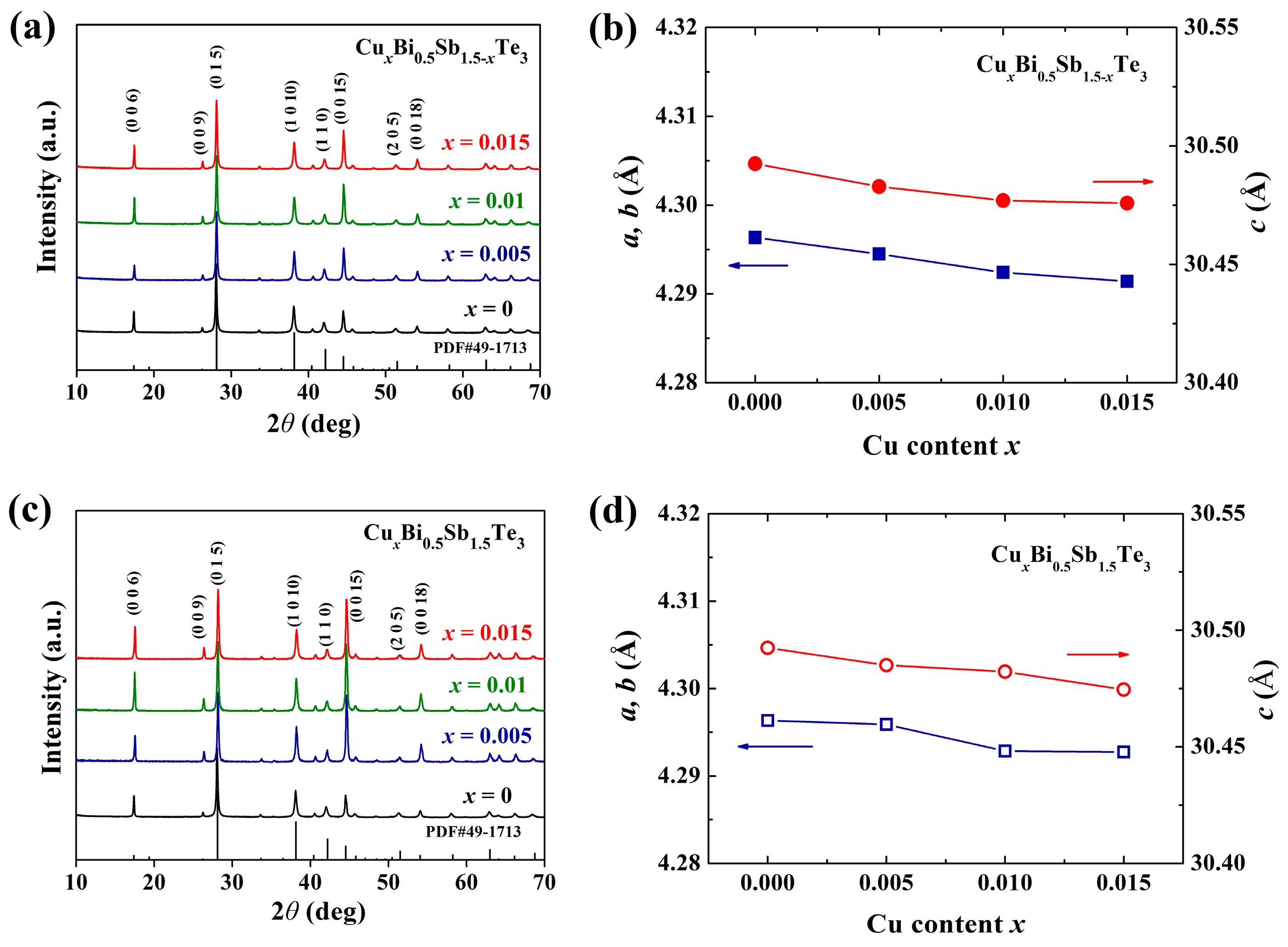
Figure 1a,c shows the powder XRD patterns for nominal Cu-doped Cu
xBi
0.5Sb
1.5-xTe
3 and nominal Cu-intercalating Cu
xBi
0.5Sb
1.5Te
3 samples. All the peaks are indexed with the standard Bi
0.5Sb
1.5Te
3 phase (PDF#49-1713). No obvious impurity phase is detected. We further refined the lattice parameters of these Bi
2Te
3-Sb
2Te
3-based alloys by using the Rietveld method. The results are shown in
Figure 1b,d, respectively. If the Cu atoms go into the van der Waals gaps as intercalated ions, the lattice parameter
a should be scarcely changed, but lattice parameter
c should be greatly increased [
10]. In contrast, if the Cu atoms occupy the Sb sites, both
a and
c should be decreased because the atomic radius of Cu (135 pm) is smaller than that of Sb atoms (145 pm). As shown in
Figure 1b, the monotonous reduction in
a and
c with increasing Cu content strongly suggests that Cu atoms enter the Sb sites in the Cu
xBi
0.5Sb
1.5-xTe
3 samples. Similar lattice contractions are also observed in nominal Cu-intercalating Cu
xBi
0.5Sb
1.5Te
3 samples (see
Figure 1d). Thus, the Cu atoms must be more energy favorable at Sb sites than at the van der Waals gaps in these p-type Bi
2Te
3-Sb
2Te
3-based alloys.
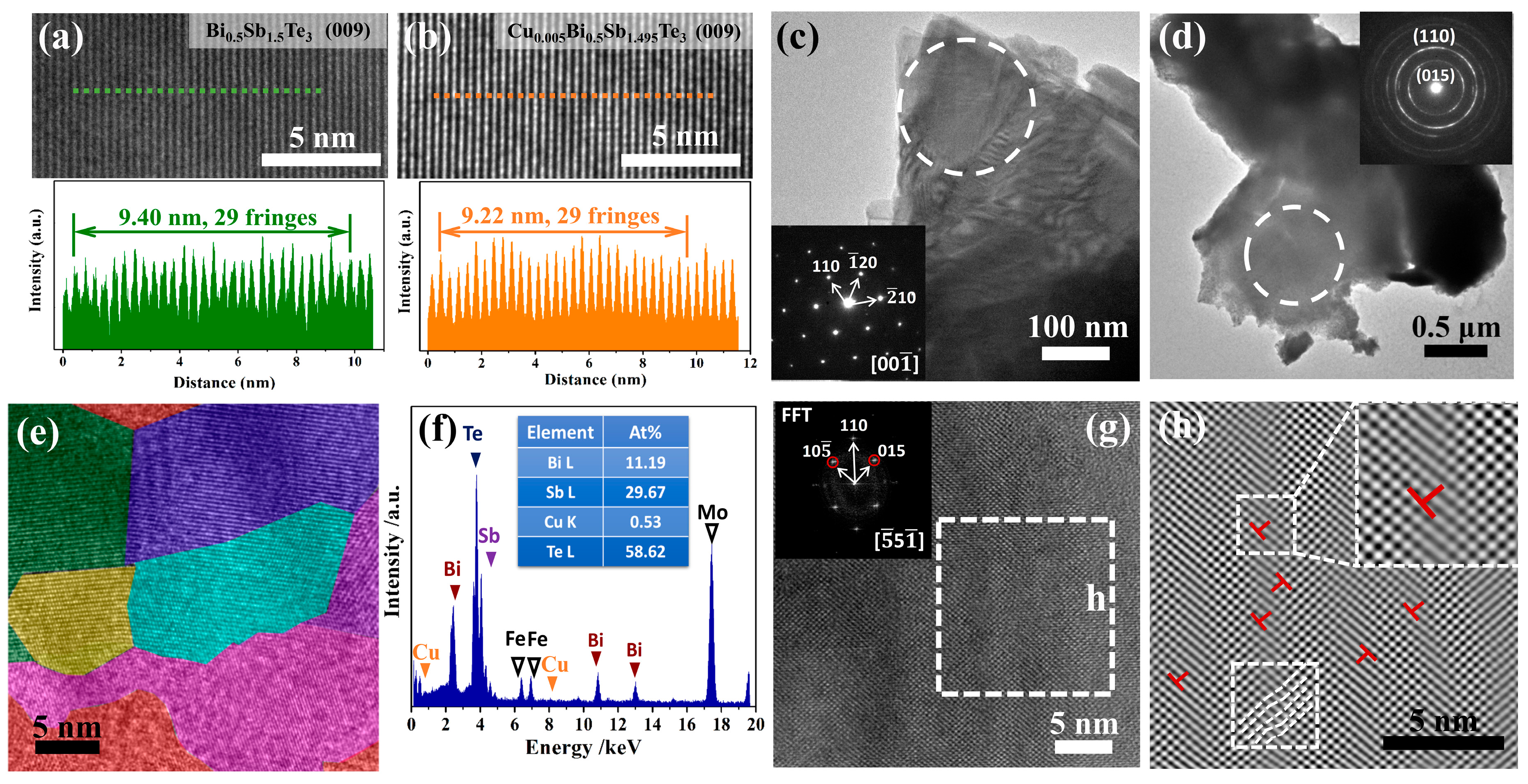
The occupying position of Cu atoms in Bi
0.5Sb
1.5Te
3 samples can also be identified by transmission electronic microscope (TEM) characterization.
Figure 2a,b displays the regular (009) plane images for Bi
0.5Sb
1.5Te
3 and Cu
0.005Bi
0.5Sb
1.495Te
3, respectively. If Cu atoms go to the van der Waals gaps, the (
00l) plane distance will be expanded, which is the scenario observed in Cu-intercalated n-type Bi
2Te
2.7Se
0.3 by Liu et al. [
10]. If Cu atoms go to the Sb sites, the (
00l) plane distance will shrink. Thus, we compared the distance of 29 fringes in the (009) plane images for both Bi
0.5Sb
1.5Te
3 and Cu
0.005Bi
0.5Sb
1.495Te
3. The total distance of these 29 fringes in Cu
0.005Bi
0.5Sb
1.495Te
3 is only 9.22 nm, which is quite smaller than that in Bi
0.5Sb
1.5Te
3 (9.40 nm). This proves that Cu atoms enter the Sb sites rather than the van der Waals gaps in the Cu
xBi
0.5Sb
1.5-xTe
3 samples, which is consistent with the contracted lattice parameters obtained by the above XRD refinement. Interestingly, these Cu atoms at Sb sites induce significant alternations on the microstructures.
Figure 2c shows the low-magnification TEM image of the undoped Bi
0.5Sb
1.5Te
3 matrix. The electron diffraction pattern obtained from the circumvented area demonstrates a typical single crystal-like character. This phenomenon is quite different from that in Cu
0.005Bi
0.5Sb
1.495Te
3. As shown in
Figure 2d, the electron diffraction pattern obtained from the circumvented area in Cu
0.005Bi
0.5Sb
1.495Te
3 shows typical polycrystalline rings, which could be indexed with standard planes in Bi
0.5Sb
1.5Te
3 system. These polycrystalline rings indicate that there are numerous nanograins inside this area. The high-magnification TEM image shown in
Figure 2e further proves that the Cu-doped material is indeed composed of nanoscale grains with coherent grain boundaries. The creation of numerous nanograins should be caused by the doped Cu atoms at the Sb sites (see the signal of Cu elements detected by energy dispersive spectrometer in
Figure 2f). The discrepancy in atomic radius between Cu
2+ (135 pm) and Sb
3+ (145 pm), as well as their different electronegativities and valence states, induce the formation of numerous lattice distortions (see
Figure 2g,h). Once the lattice distortions exceed the permitted level, dislocations and grain boundaries will be created to release the strain energy, leading to the formation of numerous nanograins, as shown in
Figure 2e. These lattice defects will strengthen the scattering to low-frequency heat-carrying phonons, which is expected to greatly lower the lattice thermal conductivity. Theoretically, various kinds of defects—such as antisite defect, dislocation, and/or vacancies—may exist in Bi
2Te
3-Sb
2Te
3-based materials [
14]. However, in this study, we used a long annealing process time to try to obtain samples near the equilibrium state. In such a case, the formation of various defects is greatly suppressed. All our data show that the Cu atoms are mainly doped at the Sb sites and promote nanocrystallization.
The bismuth telluride-based materials possess a typical layered crystal structure, and thus the sintered polycrystalline samples usually show oriented plane alignment and anisotropic TE transport properties [
15]. In this manuscript, we will just show the electrical and thermal transports along the direction parallel to the sintering press because this direction shows better TE properties.
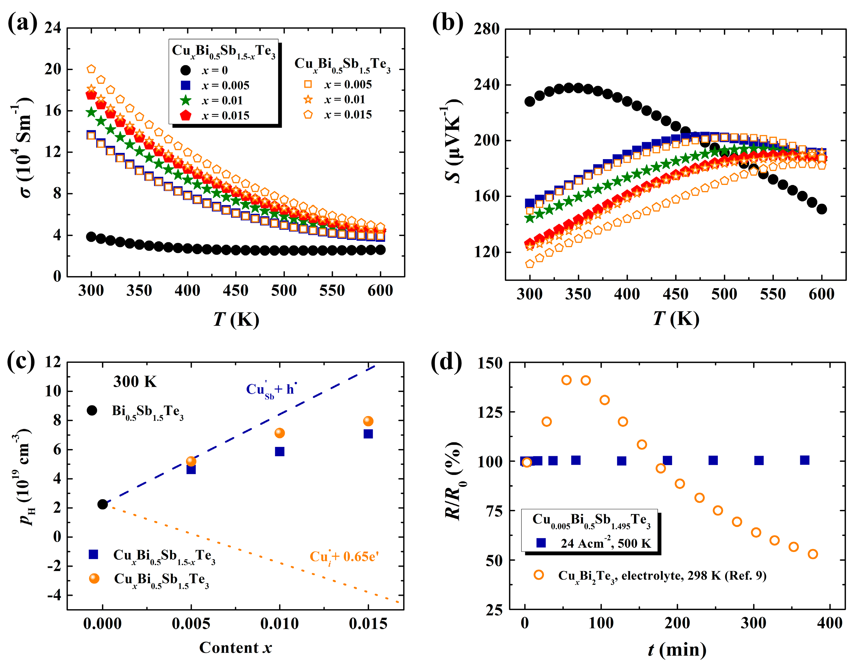
Figure 3a–c shows the electrical transport properties for all Cu
xBi
0.5Sb
1.5-xTe
3 samples. With increasing Cu content, the
σ values are gradually increased. At 300 K, the
σ for Cu
0.005Bi
0.5Sb
1.495Te
3 is about 13.7 × 10
4 Sm
−1, almost 3.5 times larger than that in the matrix compound. Correspondingly, the
S values near room temperature are greatly reduced in Cu-containing samples. Moreover, in the Cu
xBi
0.5Sb
1.5-xTe
3 system, the peak temperature of
S is shifted to higher temperatures for the sample with greater Cu content. In p-type Bi
0.5Sb
1.5Te
3 materials, if Cu atoms substitute the Sb atoms, the hole concentration should be enhanced because Cu has fewer electrons in the outermost orbital than Sb (see the dashed line in
Figure 3c). This speculation is consistent with the measurement results (square symbols) presented in
Figure 3c, which shows that the Hall hole concentration
increases when increasing the Cu-doping content. For comparison, we also show the
S,
σ, and
data for the nominal Cu-intercalated Cu
xBi
0.5Sb
1.5Te
3 samples in
Figure 3a–c. Furthermore, the measured electrical transports in Cu
xBi
0.5Sb
1.5Te
3 go against the expectation that the Cu atoms enter the van der Waals gap and introduce additional electrons (0.65 electrons per Cu atom) to reduce
and
σ (see the dotted line in
Figure 3c) [
9]. Thus, the presented electrical transport properties further prove that Cu atoms are doped at the Sb sites in p-type Bi
0.5Sb
1.5Te
3. These Cu-dopants can suppress the intrinsic excitation and shift its occurring temperature to high temperatures, thereby leading to the improved
S values in Cu-containing samples above 500 K (see
Figure 3b).
In bismuth telluride-based materials, the intercalated Cu atoms in the van der Waals gap usually form very weak interactions with the nearby Te atoms because the Te atoms do not have extra free electrons. McCarthy et al. [
9] found that the external electrical field could easily drive the Cu ions into the van der Waals gap of p-type Bi
2Te
3. However, these Cu ions will quickly diffuse out from the material when the external electrical field is removed. Interestingly, in the present Cu
xBi
0.5Sb
1.5-xTe
3 samples, the doped Cu atoms at the Sb sites have quite high stability under external electric field. We have stressed an external current of 24 Acm
−2 on the Cu
0.005Bi
0.5Sb
1.495Te
3 sample at 500 K to check its stability. If Cu atoms are intercalated in the van der Waals gap, such a large current density will definitely drive the Cu ions out from the van der Waals gap and then change its resistivity. This method has been successfully applied to characterize the Cu-ion migration behavior in Cu
2S ionic conductor [
16]. As shown in
Figure 3d, under a current density of 24 Acm
−2, the resistance of the Cu
0.005Bi
0.5Sb
1.495Te
3 sample is scarcely changed, proving that the Cu atoms have high stability under an external electric field. The Cu atoms occupying Sb sites could form strong chemical bonds with surrounding Te atoms, resulting in the observed high stability.
The tiny amount of Cu dopants in Bi
0.5Sb
1.5Te
3 scarcely changes the band structure. In principle, the density-of-states effective mass
m* that reflects band structure can be simulated by the single parabolic (SPB) model as shown below [
17]:
Here,
kB is the Boltzmann constant,
e is the elementary charge,
η is the reduced Fermi level, and
λ is the scattering parameter and taken as −1/2 for electron-phonon scattering [
18].
Fj is the Fermi integrals calculated by Equation (2). In Equation (3),
p is the hole concentration and taken as the measured
pH value, and
h is the Planck constant.
Figure 4a presents the theoretical Pisarenko plot at 300 K by assuming
m* = 1.3
me (
me is the inertia mass of electron). The experimental
S data for Cu-doped Bi
0.5Sb
1.5Te
3 samples, Cd-doped samples, and some other Bi
0.5Sb
1.5Te
3 samples previously reported will fall on this calculated line [
19,
20,
21,
22,
23], suggesting that all samples possess similar
m*. This is reasonable, considering the very tiny amount of Cu- or Cd-doping content used in the present study. These dopants just shift the Fermi level downward without obviously changing the band structure near the Fermi level.
The existence of numerous nanograins in Cu-doped samples is expected to strengthen the carrier scattering and reduce the carrier mobility (
). Surprisingly,
Figure 4b shows that the Cu-doped samples possess much higher
than the undoped Bi
0.5Sb
1.5Te
3. At room temperature,
for Cu
0.005Bi
0.5Sb
1.495Te
3 is 182.6 cm
2V
−1S
−1, which is about 70% higher than that of the undoped Bi
0.5Sb
1.5Te
3. Especially, such enhanced
values are observed over the entire measured temperature range. These enhanced carrier mobilities might benefit from the weakened ionized impurity scattering and acoustic phonon scattering. Generally, the total mobility
μ, including these two scattering mechanisms, satisfy the Matthiessen’s rule [
24]:
where
and
is the mobility for ionized impurity scattering and acoustic phonon scattering, respectively. Even in the Bi
0.5Sb
1.5Te
3, the ionized impurity scattering still exists, because there are numerous intrinsic antisite defects (
) or vacancies in the material due to their low formation energies [
14]. Generally, the corresponding mobility (
) of ionized impurity scattering could be expressed as [
25]:
Herein,
ε is the dielectric constant and taken as 75 [
26]. The relation between density-of-states effective mass
m* and single valley effective mass
satisfies
, where
Nv is valence band degeneracy and taken as 6 for Bi
2Te
3-based materials [
5,
27].
NI is the ionized impurity concentration. Dimensionless
in Equation 5 can be expressed as:
where
is reduced Planck constant.
is Debye screen length, with the formula:
The shorter
LD means a smaller Coulomb potential around ionized impurity and thereby a weaker effect on the carrier transports [
25]. Based on the Equations (5)–(7),
is simultaneously determined by the ionized impurity concentration
NI and Debye screen length
LD. As shown in
Figure 4c, the
LD value in the Bi
0.5Sb
1.5Te
3 sample is around 21.9 Å at 300 K. However, in the Cu
xBi
0.5Sb
1.5-xTe
3 samples, the
LD values are reduced to 12.3–15.2 Å, depending on the hole concentrations. Thus, although Cu-doping slightly increases
NI, the reduced
LD still leads to the weakened ionized impurity scattering to the carriers.
Besides the ionized impurity scattering, the acoustic phonon scattering to the carriers is also weakened in the Cu-doped samples. As shown in
Figure 4b, the acoustic phonon scattering (
∝
T−3/2) is the dominant scattering mechanism for all Cu
xBi
0.5Sb
1.5-xTe
3 samples around room temperature. The mobility (
) for acoustic phonon scattering in the SPB model can be written as [
27]:
where
ρ is density,
ν is the longitudinal velocity of sound and taken as 2884 m/s [
28], and
EAC is the deformation potential, which is generally used to evaluate the intensity of electron–phonon interaction.
in Equation (8) is a monotonous decreasing function with reduced Fermi level (
η) or hole concentration. It can be expressed as:
Herein, the increased hole concentration by Cu doping reduces
and thus carrier mobility with the magnitude within 9%–25% as compared with undoped matrix. However, by using the
data at 300 K, Equations (8) and (9) (see
Figure 4d) show that Cu-doping reduces the deformation potential
EAC from 18.7 eV to 14.2 eV, which could enhance mobility by more than 70%. Thus, these two effects show that the interaction between carriers and phonons is greatly lessened in Cu-doped samples. Combining the weakened ionized impurity scattering mentioned above, the enhanced carrier mobilities, observed in
Figure 4b, in Cu-doped samples can be well explained. As shown in
Figure 4c–d, the reduced
LD and
EAC can also account for the abnormal enhanced carrier mobilities in the Cd-doped Cd
xBi
0.5Sb
1.5-xTe
3 system.
Figure 5a displays the temperature dependence of total thermal conductivity
κ for Cu-doped Cu
xBi
0.5Sb
1.5-xTe
3 samples. The
κ includes three parts, termed as the carrier thermal conductivity (
κe), lattice thermal conductivity (
), and bipolar thermal conductivity (
).
κe is calculated according to Wiedemann–Franz law (
κe =
LσT, where
L is the Lorenz number and taken as 1.6 × 10
–8 V
2K
–2) [
29]. In this system, the substitution of Cu at the Sb sites significantly improves the electrical conductivity by simultaneously enhancing
and
. Thus, the
κe in Cu-doped samples is much higher than that in Bi
0.5Sb
1.5Te
3 matrix. Then, although the
values in Cu-doped samples are reduced, the total
κ near room temperature is enhanced. Because Bi
0.5Sb
1.5Te
3 has a very narrow band gap, around 0.2 eV, electrons are easily excited from the valence band to conduction band to form hole–electron pairs. The recombination of these hole–electron pairs releases extra heat and induces the remarkable
in the Cu-free Bi
0.5Sb
1.5Te
3 sample above 350 K. Doping Cu into the system effectively suppresses the
via reducing minor carrier concentration (electrons) [
8], which can account for the observed low
κ values at high temperature in Cu-doped Bi
0.5Sb
1.5Te
3 samples.
The very low
values approaching the theoretical minimum value (0.31 Wm
−1K
−1) in Cu-doped Bi
0.5Sb
1.5Te
3 samples are very interesting [
30]. We fitted the low-temperature
of Bi
0.5Sb
1.5Te
3 and Cu
0.01Bi
0.5Sb
1.49Te
3 by the Debye model, in which
is expressed by [
31]:
and the spectral lattice thermal conductivity
κs can be expressed by [
32]:
where average sound speed
ν is taken as 2930 m/s [
33]. In this equation,
, and
ω is the phonon frequency. The total relaxation time for Bi
2Te
3-based materials is given by:
where
θD is Debye temperature and taken as 160 K [
33].
,
, and
are the relaxation time for grain boundary scattering (GB), point defect scattering (PD), and phonon–phonon Umklapp scattering (U), respectively [
34].
d is the grain size, and
P and
U are the coefficients to evaluate the intensity of each phonon scattering mechanism. By fitting the low-temperature
, these parameters can be obtained (see
Table 1).
Figure 5d shows the integral area of reduced
by each individual scattering mechanism. Because the exotic Cu atoms interrupt the periodicity of lattice vibration (see the TEM results shown in
Figure 2) and bring stronger anharmonicity, the integral area of reduced
by U process is greatly reduced. Thus, the total
in Cu
0.01Bi
0.5Sb
1.495Te
3 is much lower than the Cu-free Bi
0.5Sb
1.5Te
3.
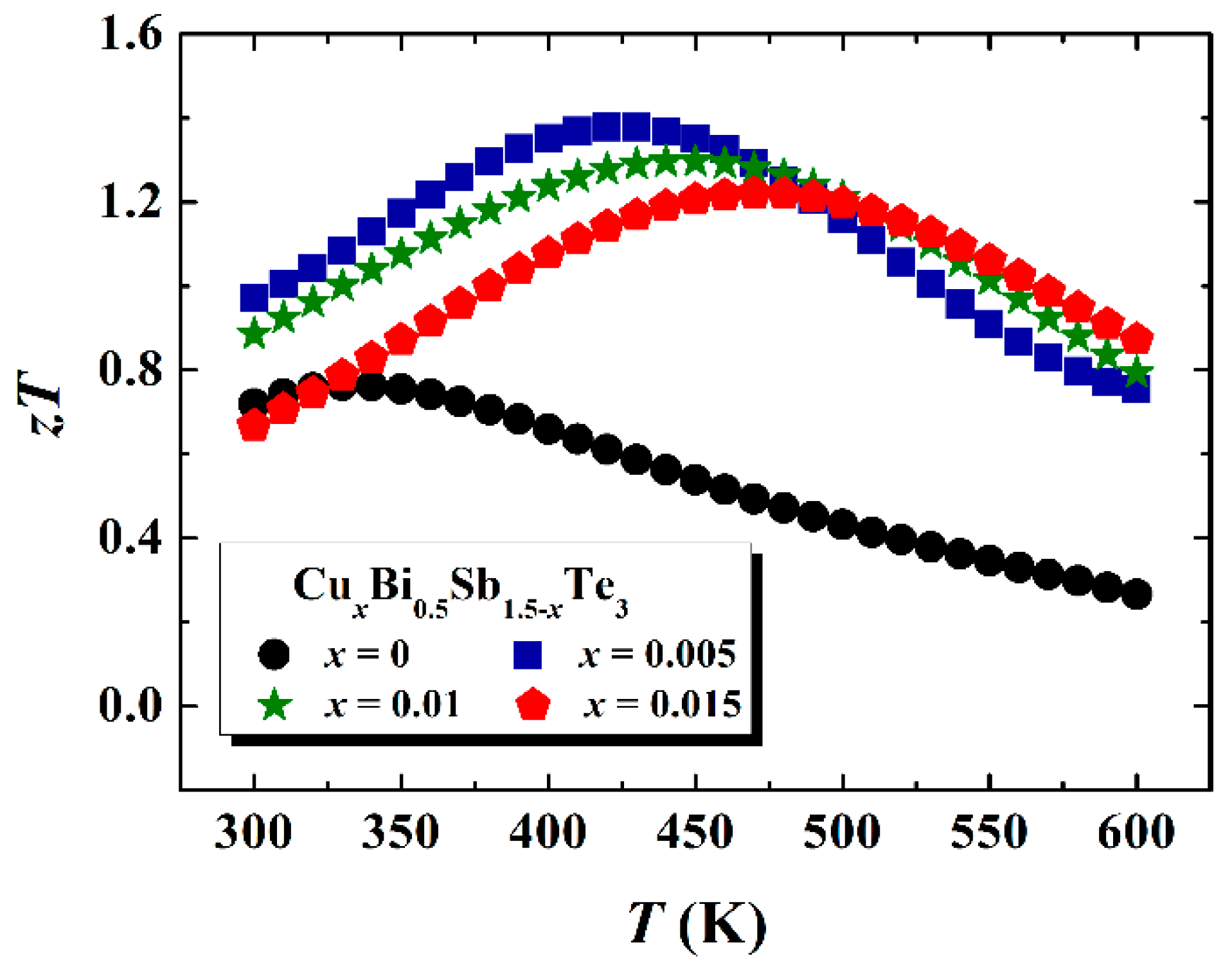
Figure 6 shows the temperature dependence of TE figure of merit
zT for Cu-doped Cu
xBi
0.5Sb
1.5-xTe
3 samples. The undoped Bi
0.5Sb
1.5Te
3 matrix displays a maximum
zT around 0.8 at 330 K. Due to the combined effects of enhanced hole concentration, improved carrier mobility, reduced lattice thermal conductivity, and bipolar thermal conductivity, the maximum
zT is significantly improved to 1.4. In addition, the suppressed intrinsic excitation in Cu-doped Cu
xBi
0.5Sb
1.5-xTe
3 successfully shifts the peak
zT towards high temperatures of 430–470 K. Combining the good stability under electric field, these Cu-doped Cu
xBi
0.5Sb
1.5-xTe
3 samples show great potential in applications such as low-grade waste heat recovery.
3. Materials and Methods
High purity elements Bi (99.999%), Sb (99.999%), Te (99.999%), Cu (99.999%), and Cd (99.999%) were used to synthesize the samples according to the stoichiometric composition CuxBi0.5Sb1.5-xTe3 (x = 0.005, 0.01, 0.015,) and CdxBi0.5Sb1.5-xTe3 (x = 0.005, 0.01, 0.015). The samples with the compositions of CuxBi0.5Sb1.5Te3 (x = 0.005, 0.01, 0.015) were also prepared in this study. These elements were firstly sealed into quartz tubes in vacuum, and then melt at 1373 K for 12 h. After quenching into a water bath, they were placed into furnace again and annealed at 673 K for 5 days. Subsequently, the grown ingots were ground to fine powders in agate mortar by hand. These obtained powders were then consolidated by spark plasma sintering (SPS) to form dense cylinders with a height of about 12 mm, which are used to characterize the TE properties along the directions parallel and perpendicular to the pressing. During the sintering procedures, the powders were filled into graphite die and held at 683 K for 10 min under a pressure of 50 MPa. High densities (>98% of the theoretical density) for all sintered samples were obtained.
X-ray diffractometer (XRD, D8 ADVANCE, Bruker Co. Ltd., Karlsruhe, Germany) was used to analyze phase purity for powder samples. The microstructures of the prepared powder samples were also observed by high-resolution transmission electronic microscope (HRTEM, JEOL 2100F, Tokyo, Japan). The chemical composition was analyzed by equipped energy dispersive spectrometer (EDS, Oxford Instruments plc, Oxfordshire, UK). Electrical conductivity (σ) and Seebeck coefficient (S) above the room temperature were measured by using commercial ZEM-3 (ULVAC Co. Ltd, Kanagawa, Japan) apparatus. The stability under large current density was evaluated by in situ measured resistance in a modified thermal dilatometer (DIL 402c, Netzch Co. Ltd., Selb, Germany). Thermal conductivity (κ) is the product of thermal diffusivity (D), heat capacity (Cp), and density (ρ). The D was measured by commercial instrument (LFA 457, Netzch Co. Ltd., Selb, Germany) based on laser flash method. The Cp was measured by using differential scanning calorimetry (DSC 200 F3, Netzch Co. Ltd., Selb, Germany). The ρ was measured by the Archimedes method. The low-temperature Hall coefficient (RH), σ, and κ were measured in Physical Property Measurement System (PPMS, Quantum Design, San Diego, CA, USA). RH was measured by sweeping magnetic field to 3 T in both positive and negative directions. The Hall carrier concentration is calculated by , and the mobility () can be estimated by .


