Article

Design of a Broadband Tunable Terahertz Metamaterial Absorber Based on Complementary Structural Graphene

1
Engineering Research Center for Metallurgical Automation and Detecting Technology Ministry of Education, Wuhan University of Science and Technology, Wuhan 430083, China
2
School of Electronic and Information Engineering, Hubei University of Science and Technology, Xianning 437100, China
3
School of Optical and Electronic Information, Huazhong University of Science and Technology, Wuhan 430074, China
*
Authors to whom correspondence should be addressed.
Materials 2018, 11(4), 540; https://doi.org/10.3390/ma11040540
Submission received: 29 January 2018 / Revised: 25 March 2018 / Accepted: 26 March 2018 / Published: 31 March 2018
(This article belongs to the Section Advanced Materials Characterization)

Abstract

:
We present a simple design for a broadband tunable terahertz (THz) metamaterial absorber (MMA) consisting of a complementary cross-oval-shaped graphene (CCOSG) structure and dielectric substrate placed on a continuous metal film. Both numerical simulation and theoretical calculation results indicate that the absorbance is greater than 80% from 1.2 to 1.8 THz, and the corresponding relative bandwidth is up to 40%. Simulated electric field and power loss density distributions reveal that the broadband absorption mainly originates from the excitation of continuous surface plasmon resonance (SPR) on the CCOSG. In addition, the MMA is polarization-insensitive for both transverse-electric (TE) and transverse-magnetic (TM) modes due to the geometry rotational symmetry of the unit-cell structure. Furthermore, the broadband absorption properties of the designed MMA can be effectively tunable by varying the geometric parameters of the unit-cell and chemical potential of graphene. Our results may find promising applications in sensing, detecting, and optoelectronic-related devices.

1. Introduction

Metamaterial absorbers (MMAs) as the engineered sub-wavelength periodic structures or functional materials have recently attracted tremendous attention in terahertz (THz) spectroscopy, since THz electromagnetic (EM) waves can be successfully absorbed by few natural materials [1,2,3,4,5,6,7,8,9,10,11,12,13,14,15,16,17,18]. Due to extensive applications in sensing [19], detection [20], modulation [21], thermal emission [22], and so on, a variety of THz MMAs have been proposed and investigated. However, most traditional MMAs have some drawbacks in that the absorption level and working frequency are uncontrolled apart from changing the geometrical parameters of the unit-cell structure, which will limit their practical applications [1,2,3,4,5,6,7,8,9,10,11,12,13,14]. Nowadays, to achieve tunable properties of the MMAs, some effective methods have been proposed and demonstrated, such as machine [23], laser [24,25,26], temperature [27,28], and voltage modulation [29,30,31,32,33,34,35]. However, the realization of the broadband tunable and strong absorption of the MMA is still a great challenge. Thus, it is still highly desirable to explore new modulation methods and design tunable MMAs with high performance.
Graphene, as a novel mono-layer two-dimensional material consisting of carbon atoms array, has the favorable electric characteristic that the conductivity depends on chemical potential (μc) being continuously tuned by chemical doping and bias voltage [36,37]. This unique characteristic makes graphene a desirable candidate to design tunable MMA. Based on effective media theory, the complex permittivity ε(ω) and permeability μ(ω) of these MMAs can be changed when the conductivity of graphene sheet is effectively controlled by gate voltage or chemical doping [24]. Recently, some MMA-based-graphene have been proposed, which can achieve strong and tunable absorption by changing the chemical potential (μc) [30,31,32,33,34,35,38,39,40,41,42,43,44,45]. According to the well-known Kubo formula, the real part of permittivity of a graphene sheet is negative from THz to optical frequencies [30]. This means that the strong surface plasmons (SPs) can be sustained, propagating along the sheet in our interesting frequency region [37,46]. In addition, SPRs will be excited when the value of the wave vector (kG) in graphene is close to the incident EM wave vector (k0) [38]. Surface plasmons resonances (SPRs) could be effectively excited in a graphene sheet as that is one key to obtaining strong absorption properties [31,32,38,39]. Zhu et al. proposed a MMA using a periodic array of graphene ribbons to achieve the tunability of absorption peak frequency in THz region [31]. However, it worked only in a narrow band range. Gao et al. presented a tunable broadband THz absorber with a graphene sheet sandwiched between periodical arrays of dielectric bricks and dielectric substrate [38]. Xiao et al. designed a multilayer cross-shaped graphene structure MMA that can achieve tunable broadband absorption in the THz region [39]. Nevertheless, the above mentioned multiband or broadband THz MMAs based on structural or patterned graphene are usually discontinuous or multilayer, which causes complexity of fabrication in practical applications. In addition, it is difficult to tune the conductivity of graphene via extra bias voltage [35,39,41].
In this work, we proposed a simple design for a broadband tunable MMA based on a periodical single-layered complementary cross-oval-shaped graphene (CCOSG) structure in the THz region. The simulation results indicate that the designed MMA can achieve strong absorption (over 80%) from 1.2 to 1.8 THz when μc is 0.5 eV. The designed MMA based on structured graphene could significantly enhance the absorption level compared with one using a single-layer graphene sheet [30]. In addition, the MMA is polarization-insensitive and the absorption of full bandwidth at half maximum (FWFH) could be shifted from 0.92–1.68 THz to 1.20–1.96 THz when μc is increased from 0.3 to 0.7 eV.

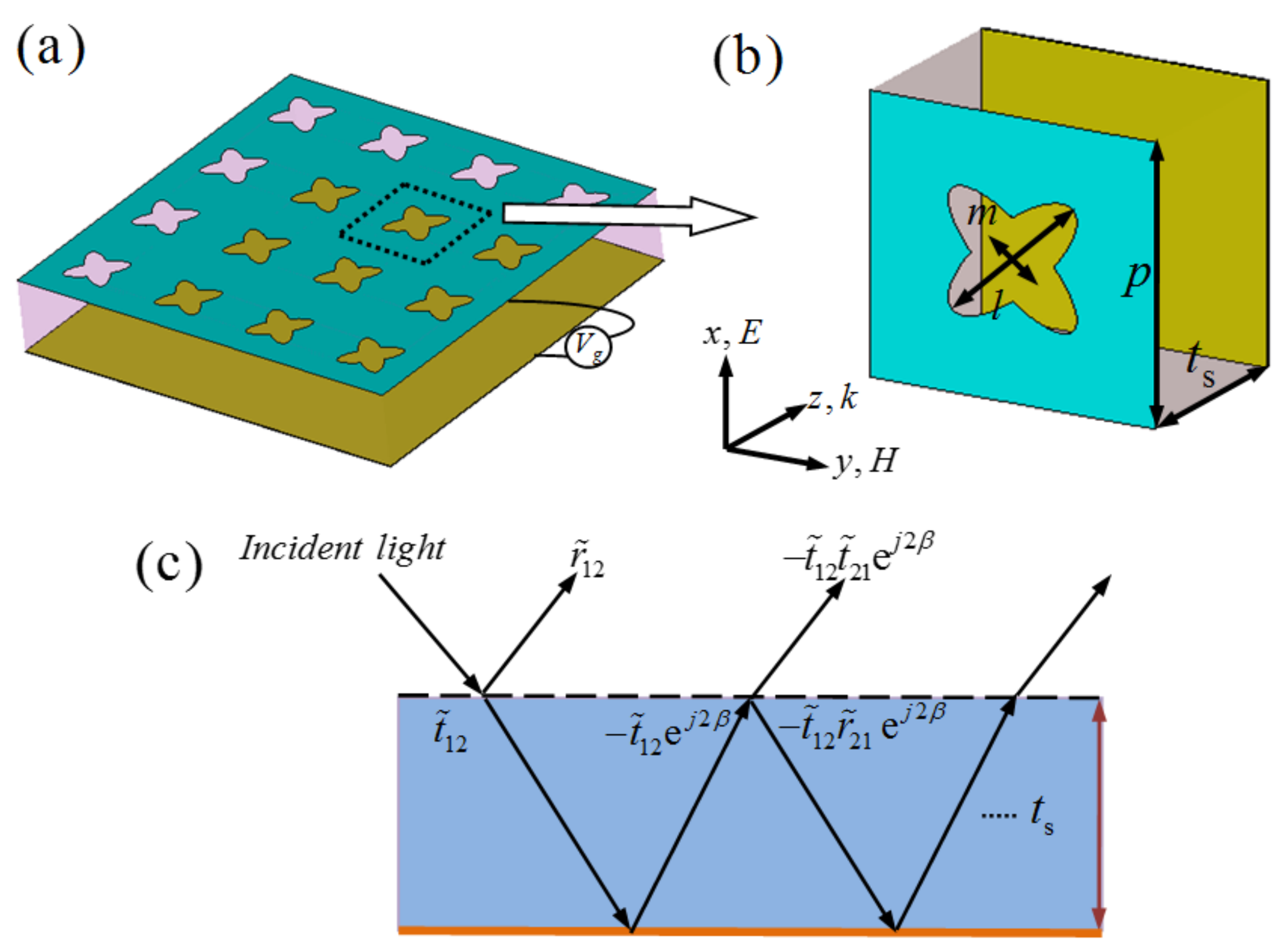
2. Structure Design, Theory, and Simulation

Figure 1a,b shows the design scheme of MMA composed of a single-layer periodical CCOSG sheet deposited on a loss-free dielectric substrate (SiO2) with a continuous metal (Cu) film on the bottom. As shown in Figure 1a,b, the period of unit-cell structure is p = 50 μm. The long and short radius of the complementary oval structure are l = 30 μm and m = 11 μm, respectively. The loss-free SiO2 with the thickness of ts = 34 μm and relative permittivity of εr = 3.9 is selected as the middle dielectric substrate. The thickness and conductivity of bottom copper film are tm = 0.5 μm and σ = 5.8 × 10⁷ S/m, respectively. Similar to previous research [45], we assume an effective thickness tg = 1 nm for a graphene sheet consisting of a mono-layer carbon atoms array in our design.
Furthermore, as shown in Figure 1a, the three-layer structure of the MMA is similar to a Fabry–Pérot resonance cavity, which can induce destructive and constructive interferences and finally result in multiple reflections and transmissions for the incident THz waves. Here, we can adopt the multiple interference theory analyze the absorption properties. As shown in Figure 1a, the multi-reflection interference model contains two interfaces: air–spacer with periodical CCOSG array, and spacer–substrate. In this design, the near-field coupling effect between the CCOSG sheet and ground plane can be neglected, since the thickness of the dielectric substrate is large enough. As shown in Figure 1c, when the incident THz wave enters the MMA, part is reflected at the CCOSG–air interface, and the other part emits from the interface after multiple reflections and transmissions. Thus, the overall reflection coefficient of the structure is expressed as follows [14]:
r ˜ a l l = r ˜ 12 t ˜ 12 t ˜ 21 e j 2 β 1 + r ˜ 21 e j 2 β ,
where β = nk0ts is the propagation phase, n and ts are the refractive index and thickness of dielectric substrate SiO2, respectively, and k0 is the free space wave number. In addition, r ˜ 12 and t ˜ 12 represent the reflection and transmission coefficient at the air–CCOSG interface, respectively. At the CCOSG–substrate interface, the corresponding reflection and transmission coefficients can be defined by r ˜ 21 and t ˜ 21 , respectively. Therefore, the total absorbance can be derived by A(ω) = 1 − | r ˜ a l l |2.
To realize the tunability of the proposed MMA, we added the external bias voltage to the MMA, as shown in Figure 1a. Based on previous studies [32,47], the chemical potential (μc) could be controlled by bias voltage:
μ c = v f π ε 0 ε r V g e t s ,
where vf is Fermi velocity, ε0 is the vacuum permittivity constant, e is an electron charge constant, ћ is the reduced Planck’s constant, μc is chemical potential, and Vg is the extra bias voltage. We assume that the working frequency range is 0.5–2 THz, and the chemical potential of the graphene sheet is 0.3 to 0.7 eV [38]. According to the well-known Kubo formula, the conductivity model of graphene sheet can be simplified as follows [37,48]:
σ g j e 2 K B T π 2 ( ω + j τ 1 ) ( μ c K B T + 2 ln ( e ( μ c K B T ) + 1 ) ) ,
where ω is radio frequency, T is environment temperature, τ is relaxation time, and KB is Boltzmann’s constant. The other parameters have been defined previously. In our work, T is fixed at 300 K and τ is assumed to be 0.5 ps. Thus, the relative permittivity of graphene can be obtained by εg = 1 + g/ωε0tg [35].
To study the efficiency of the proposed MMA, the CST microwave studio based on finite integration technique (FIT) is employed to perform full-wave simulation. In the simulation, the periodic boundary conditions are used in the x-y plane and incident THz waves propagate along the z-direction, as shown in Figure 1a,b. The electric and magnetic components of the incident THz wave are along the x and y direction, respectively, and the wave vector k is along the z-direction, as depicted in Figure 1b. The absorbance is calculated by A(ω) = 1 − R(ω) − T(ω), where R(ω) and T(ω) are the reflectance and transmittance, respectively. Because the thickness of the bottom continuous copper film is much greater than skin depth in our frequency range of interest, the incident light is prevented through the whole MMA and the transmittance can be ignored. Thus, the absorbance can be rewritten as A(ω) = 1 − R(ω).

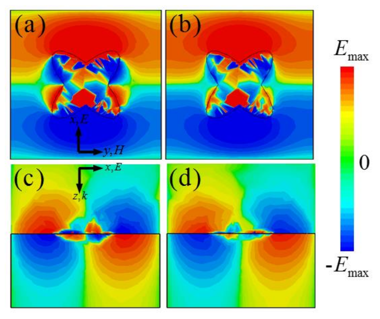
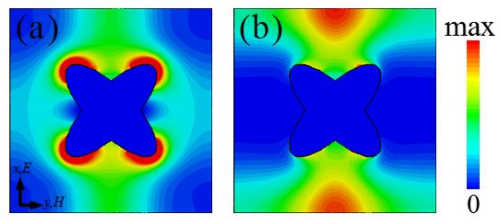
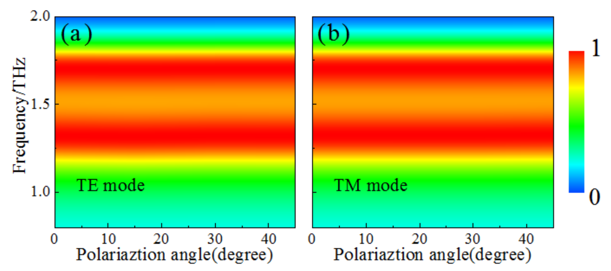
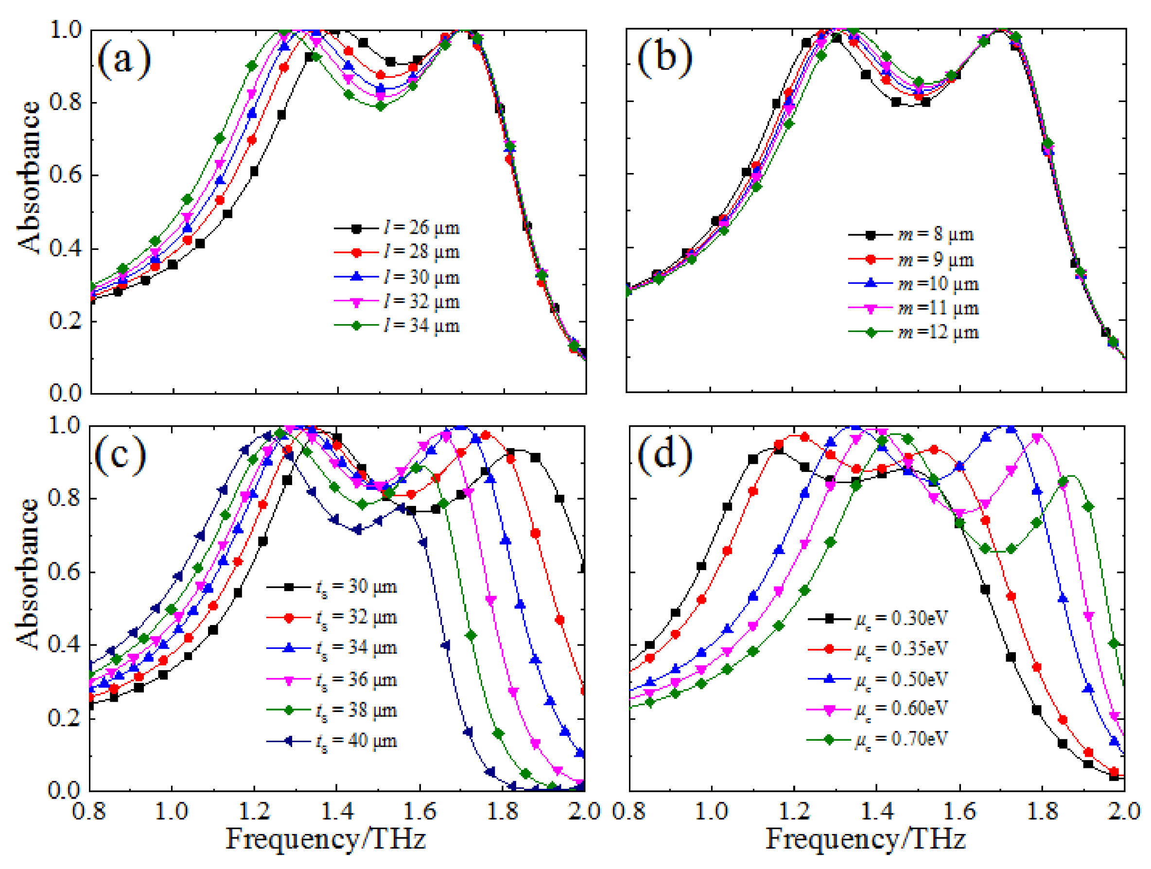
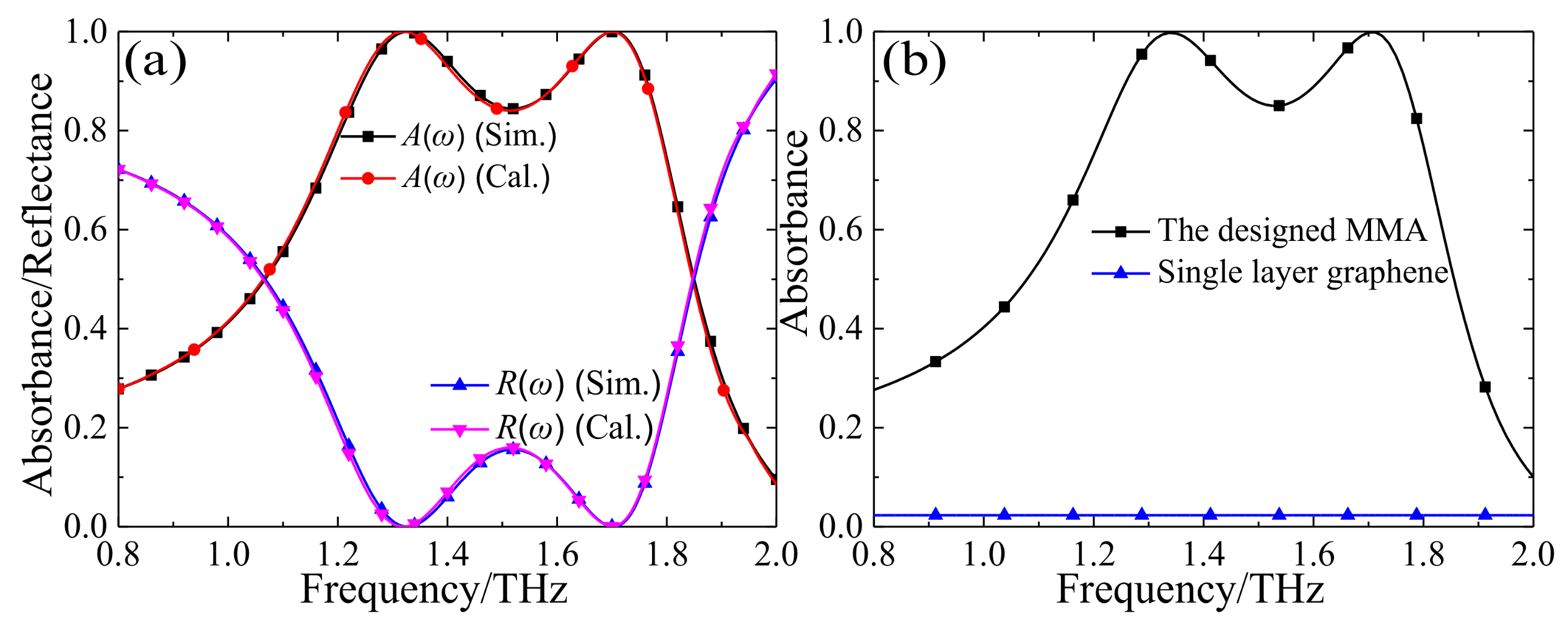
3. Results and Discussion

Figure 2 shows the numerical results of the proposed MMA when the chemical potential μc is set to 0.5 eV. As depicted in Figure 2a, the simulated reflectance is below 20% from 1.2 to 1.8 THz, and the corresponding absorbance is greater than 80%. Thus, the relative stronger absorption bandwidth is up to 40%. In addition, at two resonance frequencies (f1 = 1.34 THz and f2 = 1.71 THz), the absorption levels are both greater than 99.9%. Obviously, the simulation results agree well with the calculation ones based on interference theory. Figure 2b shows the absorbance of the MMA based on the CCOSG structure and the single-layer continuous graphene sheet, respectively. It can be seen that the absorption level of the single-layer continuous graphene sheet is very small (about only 2.3%), and far less than that of the MMA based on the CCOSG structure. Thus, the high absorption level of the MMA with CCOSG structure design can be significantly enhanced for the incident THz waves [49].
To better understand the physical mechanism of the stronger absorption behavior observed in the broadband, the electric field (Ez) distributions of the xy and xz planes of the unit-cell structure at two resonance frequencies are investigated numerically. Figure 3a,b shows that the electric field (Ez) distributions mainly concentrate on the four corners of the CCOSG structure and the upper and lower sides of unit-cell structure. As shown in Figure 3c,d, surface plasmon polaritons (SPPs) are effectively excited at two absorption peak frequencies (f1 = 1.34 THz, f2 = 1.71 THz). Since strong absorption is obtained, kG is about equal to k0 and SPRs are excited between f1 and f2. In addition, it can be observed that fundamental and second-order SPR are effectively excited at two resonance frequencies. Furthermore, since the dielectric substrate is loss-free and incident light is less absorbed by a single-layer graphene sheet in a broadband range, it can be conjectured that the strong SPRs noticeably enhance the absorption efficiency of the CCOSG structure of this MMA. However, there is a small difference in the field distributions for two resonance frequencies. Compared with the first resonance frequency, the fundamental SPR is slightly suppressed by the second-order one at the second resonance frequency.
To further understand the absorption mechanism, we give the power loss density distributions of the xy plane on the CCOSG surface at two absorption peak frequencies when μc = 0.5 eV, as shown in Figure 4. For the first absorption peak, as shown in Figure 4a, the THz energy is mainly dissipated at the four corners of the CCOSG structure, meaning that the absorption is principally based on fundamental SPR. However, as shown in Figure 4b, there are power losses at the upper and lower edges of the unit-cell structure at the second resonance frequency. The absorption mainly originates from excitation of second-order SPR at the second absorption peak. Thus, the loss density distributions further illustrate that the broadband absorption of this designed MMA is based on effective excitation of the fundamental and second-order SPRs.
Polarization insensitivity is of considerable merit for MMAs in practical applications. Thus, it should be considered for our design under different polarization angles for both TE and TM modes. Owing to the rotation symmetry of the unit-cell structure, the absorption spectra of the designed MMA are basically unchanged when the polarization angle is from 0 to 45° for both TE and TM modes, as shown in Figure 5a,b.
Taking things a step further, we also study the resonance absorption properties of the designed MMA with different geometric parameters for the unit-cell structure and chemical potential (μc). As shown in Figure 6a, when the long radius (l) of the CCOSG structure increases from 26 to 34 μm, the strong absorption bandwidth is extended and the absorption level at the central frequency is gradually decreased. In addition, the first absorption is red-shifted from 1.4 to 1.27 THz and the second absorption peak is basically unchanged. Meanwhile, the proposed MMA maintains perfect absorption at two resonance frequencies. However, the case is much different for the short radius (m) of the CCOSG structure, as shown in Figure 6b. When m increases from 8 to 12 μm, the strong absorption bandwidth becomes narrower and the absorption level gradually increases at the central absorption frequency. In addition, the first absorption peak frequency is slightly blue-shifted from 1.27 to 1.34 THz, but the second is nearly unchanged. Similarly, the absorption level also achieves 99% at two resonance frequencies. It should be noticed that only the first resonance frequency is affected by changing l and m, since the incident THz wave energy is mainly dissipated at the four corners of the CCOSG structure at the first resonance frequency (see Figure 4a). Considering that the first SPR is localized at the four corners, the dispersion relation can be approximated for the localized SPR, which is matched with the simulation results [46]. The second SPR, which is excited in the graphene sheet with no gap, is nearly unchanged with different l or m. Based on SPRs in unstructured graphene sheets, the second SPR frequency is relative to μc [38]. Thus, the first resonance frequency and bandwidth are dynamically modulated by tuning the l or m value of the CCOSG structure.
Then, as shown in Figure 6c, when the thickness (ts) of the dielectric substrate increases from 30 to 40 μm, the frequency range of strong absorption is decreased and gradually red-shifted. In this case, two resonance absorption frequencies decrease gradually from 1.37 to 1.22 THz, and from 1.84 to 1.56 THz, respectively. Due to the increasing thickness of the resonant cavity, the working frequency range is gradually red-shifted, resulting in the resonance frequencies first being close to the central strong SPR range and then deviating from it [50]. Thus, the absorption level first increases and then decreases gradually with the increase in ts, and is at a maximum when ts = 34 μm.
Finally, the absorption properties of the proposed MMA are further discussed when the chemical potential is tuned from 0.3 to 0.7 eV through external bias voltage, as shown in Figure 6d. The frequency range of the FWHM of the designed MMA is obviously blue-shifted from 0.92–1.68 THz to 1.20–1.96 THz when μc is increased from 0.3 to 0.7 eV. According to Equation (3), the working frequency band is blue-shifted to compensate for the increased conductivity of the graphene sheet [41]. When the chemical potential is 0.3 eV, the designed MMA displays great absorption at 1.15 THz and 1.47 THz. When μc increases from 0.3 to 0.5 eV, the absorbance of MMA is gradually enhanced and finally reaches 99.9% at 1.34 THz and 1.71 THz. For higher μc, more charge carriers are needed to better excite SPRs for the normal incident THz waves. In addition, the blue-shifted frequency also contributes to inducing SPRs [51,52]. However, the absorption level will decrease gradually when further increasing μc (>0.5 eV). When μc = 0.7 eV, the two resonance frequencies are shifted to 1.45 THz and 1.87 THz, and the corresponding absorbance is decreased to 97.8% and 86.38%, respectively. Since the resonance frequencies gradually deviate from the central frequency range of the strong SPR, the absorption level decreases accordingly [50]. Moreover, at the central absorption frequency, the absorption level first increases slightly when μc increases from 0.3 to 0.35 eV. When μc increases further from 0.4 eV, the absorption level of the second frequency decreases and the strong absorption bandwidth gradually broadens. Overall, the designed MMA can achieve dynamically tunable absorption by adjusting the chemical potential, which has great potential applications in THz range.

4. Conclusions

In conclusion, we have proposed a broadband tunable MMA using a CCOSG structure and a dielectric substrate placed on a metallic film in the THz region. Numerical simulation results indicate that the proposed MMA can achieve high absorption of over 80% in the frequency range of 1.2–1.8 THz, and the corresponding relative bandwidth is up to 40%, which agrees well with calculated ones based on interference theory. The distributions of electric field and power loss density of the unit-cell structure reveal that the enhancement of absorption of MMA mainly originates from the effective excitations of fundamental and second-order SPRs on the CCOSG structure. In addition, the polarization-insensitive properties of the MMA are demonstrated by a numerical simulation. Furthermore, we discussed the influence of the geometrical parameters of the unit-cell structure and external bias voltage on the absorption properties of the MMA. Compared with conventional discontinuous or multi-layered graphene structures, the proposed high-performance MMA is easily fabricated and modulated. Due to its favorable performance, the proposed tunable THz MMA could find some potential applications in thermal imaging, thermal bolometers, biosensors, and so on.

Acknowledgments

This work was supported by the National Natural Science Foundation of China (Grant nos. U1435209, 61605147 and 61701185) and the Natural Science Foundation of Hubei China (Grant no. 2017CFB588).

Author Contributions

Mu Lin Huang and Yong Zhi Cheng conceived and designed the experiments; Zheng Ze Cheng and Hao Ran Chen performed the experiments; Mu Lin Huang and Xue Song Mao analyzed the data; Rong Zhou Gong contributed reagents/materials/analysis tools; Mu Lin Huang and Yong Zhi Cheng wrote the paper.

Conflicts of Interest

The authors declare no conflict of interest.

References

  1. Landy, N.I.; Sajuyigbe, S.; Mock, J.J.; Smith, D.R.; Smith, D.R. Perfect metamaterial absorber. Phys. Rev. Lett. 2008, 100, 207402. [Google Scholar] [CrossRef] [PubMed]
  2. Cao, T.; Wei, C.; Simpson, R.E.; Zhang, L.; Cryan, M.J. Broadband Polarization-Independent Perfect Absorber Using a Phase-Change Metamaterial at Visible Frequencies. Sci. Rep. 2014, 4, 3955. [Google Scholar] [CrossRef] [PubMed]
  3. Tao, H.; Bingham, C.M.; Strikwerda, A.C.; Pilon, D.; Shrekenhamer, D.; Landy, N.I.; Fan, K.; Zhang, X.; Padilla, W.J.; Averitt, R.D. Highly flexible wide angle of incidence terahertz metamaterial absorber: Design, fabrication, and characterization. Phys. Rev. B 2008, 78, 241103. [Google Scholar] [CrossRef]
  4. Wang, G.D.; Liu, M.H.; Hu, X.W.; Kong, L.H.; Cheng, L.L.; Chen, Z.Q. Broadband and ultra-thin terahertz metamaterial absorber based on multi-circular patches. Eur. Phys. J. B 2013, 86, 304. [Google Scholar] [CrossRef]
  5. Pu, M.; Wang, M.; Hu, C.; Huang, C.; Zhao, Z.; Wang, Y.; Luo, X. Engineering heavily doped silicon for broadband absorber in the terahertz regime. Opt. Express 2012, 20, 25513–25519. [Google Scholar] [CrossRef] [PubMed]
  6. Huang, L.; Chowdhury, D.R.; Ramani, S.; Reiten, M.T.; Luo, S.; Taylor, A.J.; Chen, H. Experimental demonstration of terahertz metamaterial absorbers with a broad and flat high absorption band. Opt. Lett. 2012, 37, 154–156. [Google Scholar] [CrossRef] [PubMed]
  7. Wang, B.X. Quad-Band terahertz metamaterial absorber based on the combining of the dipole and quadrupole resonances of two SRRs. IEEE J. Sel. Top. Quantum Electron. 2017, 23, 4700107. [Google Scholar] [CrossRef]
  8. Grant, J.P.; McCrindle, I.J.H.; Cumming, D.R.S. Simulation, Fabrication and Characterization of THz Metamaterial Absorbers. J. Vis. Exp. 2012, 70, 50114. [Google Scholar] [CrossRef] [PubMed]
  9. Ma, Y.; Chen, Q.; Grant, J.; Saha, S.C.; Khalid, A.; Cumming, D.R.S. A terahertz polarization insensitive dual band metamaterial absorber. Opt. Lett. 2011, 36, 945–947. [Google Scholar] [CrossRef] [PubMed]
  10. Cheng, Y.; Huang, M.; Chen, H.; Guo, Z.; Mao, X.; Gong, R. Ultrathin Six-Band polarization-insensitive perfect metamaterial absorber based on a cross-cave patch resonator for ferahertz waves. Materials 2017, 10, 591. [Google Scholar] [CrossRef] [PubMed]
  11. Deng, G.S.; Xia, T.Y.; Fang, Y.; Yang, J.; Yin, Z.P. A Polarization-Dependent Frequency-Selective Metamaterial absorber with multiple absorption peaks. Appl. Sci. 2017, 7, 580. [Google Scholar] [CrossRef]
  12. Cheng, Y.Z.; Cheng, Z.Z.; Mao, X.S.; Gong, R.Z. Ultra-thin multi-band polarization-insensitive microwave metamaterial absorber based on multiple-order responses using a single resonator structure. Materials 2017, 10, 1241. [Google Scholar] [CrossRef] [PubMed]
  13. Cheng, Y.Z.; Mao, Y.S.; Wu, C.J.; Wu, L.; Gong, R.Z. Infrared non-planar plasmonic perfect absorber for enhanced sensitive refractive index sensing. Opt. Mater. 2016, 53, 195–200. [Google Scholar] [CrossRef]
  14. Chen, H.T. Interference theory of metamaterial perfect absorbers. Opt. Express 2012, 20, 7165–7172. [Google Scholar] [CrossRef] [PubMed]
  15. Wen, Q.Y.; Xie, Y.S.; Zhang, H.W.; Yang, Q.H.; Li, Y.X.; Liu, Y.L. Transmission line model and fields analysis of metamaterial absorber in the terahertz band. Opt. Express 2009, 17, 20256–20265. [Google Scholar] [CrossRef] [PubMed]
  16. Amin, M.; Farhat, M.; Bagci, H. An ultra-broadband multilayered graphene absorber. Opt. Express 2013, 21, 29938–29948. [Google Scholar] [CrossRef] [PubMed]
  17. Xia, S.; Zhai, X.; Huang, Y.; Liu, J.; Wang, L.; Wen, S. Multi-band perfect plasmonic absorptions using rectangular graphene gratings. Opt. Lett. 2017, 42, 3052–3055. [Google Scholar] [CrossRef] [PubMed]
  18. Cheng, Y.; Yan, N.; Rong, G. A polarization-insensitive and omnidirectional broadband terahertz metamaterial absorber based on coplanar multi-squares films. Opt. Laser Technol. 2013, 48, 415–421. [Google Scholar] [CrossRef]
  19. Alves, F.; Grbovic, D.; Kearney, B.; Lavrik, N.V.; Karunasiri, G. Bi-material terahertz sensors using metamaterial structures. Opt. Express 2013, 21, 13256–13271. [Google Scholar] [CrossRef] [PubMed]
  20. Mittendorff, M.; Winnerl, S.; Kamann, J.; Eroms, J.; Weiss, D.; Schneider, H.; Helm, M. Ultrafast graphenebased broadband THz detector. Appl. Phys. Lett. 2013, 103, 021113. [Google Scholar] [CrossRef]
  21. Le, L.N.; Thang, N.M.; Thuy, L.M.; Tung, N.T. Hybrid semiconductor-dielectric metamaterial modulation for switchable bi-directional THz absorbers. Opt. Commun. 2017, 383, 244–249. [Google Scholar] [CrossRef]
  22. Pu, M.; Chen, P.; Wang, Y.; Zhao, Z.; Wang, C.; Huang, C.; Hu, C.; Luo, X. Strong enhancement of light absorption and highly directive thermal emission in graphene. Opt. Express 2013, 21, 11618–11627. [Google Scholar] [CrossRef] [PubMed]
  23. Hu, F.; Qian, Y.; Li, Z.; Niu, J.; Nie, K.; Xiong, X.; Zhang, W.; Peng, Z. Design of a tunable terahertz narrowband metamaterial absorber based on an electrostatically actuated MEMS cantilever and split ring resonator array. J. Opt. 2013, 15, 055101. [Google Scholar] [CrossRef]
  24. Cheng, Y.; Gong, R.; Cheng, Z. A photoexcited broadband switchable metamaterial absorber with polarization-insensitive and wide-angle absorption for terahertz waves. Opt. Commun. 2016, 361, 41–46. [Google Scholar] [CrossRef]
  25. Cheng, Y.; Gong, R.; Zhao, J. A photoexcited switchable perfect metamaterial absorber/reflector with polarization-independent and wide-angle for terahertz waves. Opt. Mater. 2016, 62, 28–33. [Google Scholar] [CrossRef]
  26. Shen, X.; Cui, T.J. Photoexcited broadband redshift switch and strength modulation of terahertz metamaterial absorber. J. Opt. 2012, 14, 114012. [Google Scholar] [CrossRef]
  27. Zhu, J.; Han, J.; Tian, Z.; Gu, J.; Chen, Z.; Zhang, W. Thermal broadband tunable Terahertz metamaterials. Opt. Commun. 2011, 284, 3129–3133. [Google Scholar] [CrossRef]
  28. Wang, B.X.; Wang, G.Z. Temperature tunable metamaterial absorber at THz frequencies. J. Mater. Sci. Mater. Electron. 2017, 28, 8487–8493. [Google Scholar] [CrossRef]
  29. Yuan, H.; Zhu, B.O.; Feng, Y. A frequency and bandwidth tunable metamaterial absorber in x-band. J. Appl. Phys. 2015, 117, 173103. [Google Scholar] [CrossRef]
  30. Xiao, B.; Gu, M.; Qin, K.; Xiao, S. Absorption enhancement in graphene with an efficient resonator. Opt. Quantum Electron. 2017, 49, 177. [Google Scholar] [CrossRef]
  31. Zhu, Z.H.; Guo, C.C.; Liu, K.; Zhang, J.F.; Ye, W.M.; Yuan, X.D.; Qin, S.Q. Electrically tunable polarizer based on anisotropic absorption of graphene ribbons. Appl. Phys. A 2014, 114, 1017–1021. [Google Scholar] [CrossRef]
  32. Ye, C.; Zhu, Z.; Xu, W.; Yuan, X.; Qin, S. Electrically tunable absorber based on nonstructured graphene. J. Opt. 2015, 17, 125009. [Google Scholar] [CrossRef]
  33. Zhang, L.; Hu, F.; Xu, X.; Wang, Y.; Guo, E. Design of separately tunable terahertz two-peak absorber based on graphene. Opt. Commun. 2016, 369, 65–71. [Google Scholar] [CrossRef]
  34. Ye, L.; Chen, Y.; Cai, G.; Liu, N.; Zhu, J.; Song, Z.; Liu, Q.H. Broadband absorber with periodically sinusoidally-patterned graphene layer in terahertz range. Opt. Express 2017, 25, 11223–11232. [Google Scholar] [CrossRef] [PubMed]
  35. Li, L.; Cao, M.; Li, T.; Meng, L.; Zhang, H.; Zhang, Y. Complementary graphene metamaterial with independently tunable dual absorption bands at terahertz frequency. Mater. Res. Express 2017, 4, 105801. [Google Scholar] [CrossRef]
  36. Novoselov, K.S.; Fal’ko, V.I.; Colombo, L.; Gellert, P.R.; Schwab, M.G.; Kim, K. A roadmap for graphene. Nature 2012, 490, 192–200. [Google Scholar] [CrossRef] [PubMed]
  37. Hanson, G.W. Dyadic Green’s functions and guided surface waves for a surface conductivity model of grapheme. J. Appl. Phys. 2008, 103, 064302. [Google Scholar] [CrossRef]
  38. Gao, F.; Zhu, Z.; Xu, W.; Zhang, J.; Guo, C.; Liu, K.; Yuan, X.; Qin, S. Broadband wave absorption in single-layered and nonstructured graphene based on far-field interaction effect. Opt. Express 2017, 25, 9579–9586. [Google Scholar] [CrossRef] [PubMed]
  39. Xiao, B.; Gu, M.; Xiao, S. Broadband, wide-angle and tunable terahertz absorber based on cross-shaped graphene arrays. Appl. Opt. 2017, 56, 5458–5462. [Google Scholar] [CrossRef] [PubMed]
  40. Andrei, A.; Andrei, L. Graphene metamaterials based tunable terahertz absorber: Effective surface conductivity approach. Opt. Express 2013, 21, 9144–9155. [Google Scholar]
  41. Su, Z.; Yin, J.; Zhao, X. Terahertz dual-band metamaterial absorber based on graphene/MgF2 multilayer structures. Opt. Express 2015, 23, 1679–1690. [Google Scholar] [CrossRef] [PubMed]
  42. Chen, M.; Sun, W.; Cai, J.; Chang, L.; Xiao, X. Frequency-tunable terahertz absorbers based on graphene metasurface. Opt. Commun. 2017, 382, 144–150. [Google Scholar] [CrossRef]
  43. Zhang, Q.; Ma, Q.; Yan, S.; Wu, F.; He, X.; Jiang, J. Tunable terahertz absorption in graphene-based metamaterial. Opt. Commun. 2015, 353, 70–75. [Google Scholar] [CrossRef]
  44. Alaee, R.; Farhat, M.; Rockstuhl, C.; Lederer, F. A perfect absorber made of a graphene micro-ribbon metamaterial. Opt. Express 2012, 20, 28017–28024. [Google Scholar] [CrossRef] [PubMed]
  45. Xing, R.; Jian, S. A dual-band THz absorber based on graphene sheet and ribbons. Opt. Laser Technol. 2018, 100, 129–132. [Google Scholar] [CrossRef]
  46. Liao, Z.; Luo, Y.; Fernandez-Domínguez, A.I.; Shen, X.; Maier, S.A.; Cui, T.J. High-order localized spoof surface plasmon resonances and experimental verifications. Sci. Rep. 2015, 5, 09590. [Google Scholar] [CrossRef] [PubMed]
  47. Liu, B.; Tang, C.; Chen, J.; Zhu, M.; Pei, M.; Zhu, X. Electrically Tunable Fano Resonance from the Coupling between Interband Transition in Monolayer Graphene and Magnetic Dipole in Metamaterials. Sci. Rep. 2017, 7, 17117. [Google Scholar] [CrossRef] [PubMed]
  48. Gusynin, P.; Sharaphov, S.G.; Carbotte, J.P. Magneto-optical conductivity in graphene. J. Phys. Condens. Matter 2007, 19, 026222. [Google Scholar] [CrossRef]
  49. Dawlaty, J.M.; Shivaraman, S.; Strait, J.; George, P.; Chandrashekhar, M.; Rana, F.; Spencer, M.G.; Veksler, D.; Chen, Y.Q. Measurement of the optical absorption spectra of epitaxial graphene from terahertz to visible. Appl. Phys. Lett. 2008, 93, 131905. [Google Scholar] [CrossRef]
  50. Thongrattanasiri, S.; Koppens, F.H.; García de Abajo, F.J. Complete Optical Absorption in Periodically Patterned Graphene. Phys. Rev. Lett. 2012, 108, 047401. [Google Scholar] [CrossRef] [PubMed]
  51. Ke, S.; Wang, B.; Huang, H.; Long, H.; Wang, K.; Lu, P. Plasmonic absorption enhancement inperiodic cross-shaped graphene arrays. Opt. Express 2015, 23, 8888–8900. [Google Scholar] [CrossRef] [PubMed]
  52. Huang, M.; Cheng, Y.; Cheng, Z.; Chen, H.; Mao, X.; Gong, R. Based on graphene tunable dual-band terahertz metamaterial absorber with wide-angle. Opt. Commun. 2018, 415, 194–201. [Google Scholar] [CrossRef]
Figure 1. The scheme of designed THz MMA: (a) the period array and (b) unit-cell structure; (c) the interference model.
Materials 11 00540 g001
Figure 2. The numerical results of the proposed MMA with μc = 0.5 eV: (a) the simulated and calculated reflectance and absorbance of the designed MMA based on CCOSG sheet; (b) the simulated absorbance of the MMA based on CCOSG sheet and bare mono-layer graphene.
Materials 11 00540 g002
Figure 3. The electric field (Ez) distributions of the xy and xz planes of the unit-cell structure at (a,c) f1 = 1.34 THz and (b,d) f2 = 1.71 THz, respectively (μc = 0.5 eV).
Materials 11 00540 g003
Figure 4. The loss density distributions of the xy plane on the CCOSG surface: (a) f1 = 1.34 THz and (b) f2 = 1.71 THz, respectively (μc = 0.5 eV).
Materials 11 00540 g004
Figure 5. The absorption spectra under different polarization angles for (a) TE and (b) TM modes.
Materials 11 00540 g005
Figure 6. The absorption spectra under different geometric parameters of the unit-cell structure and chemical potential: (a,b) the long (l) and short (m) radius of the CCOSG structure; (c) the thickness (ts) of the dielectric substrate; (d) the chemical potential (μc).
Materials 11 00540 g006

