Enhancement on the Surface Hydrophobicity and Oleophobicity of an Organosilicon Film by Conformity Deposition and Surface Fluorination Etching

Abstract
:1. Introduction
2. Material Preparation and Experimental Procedure
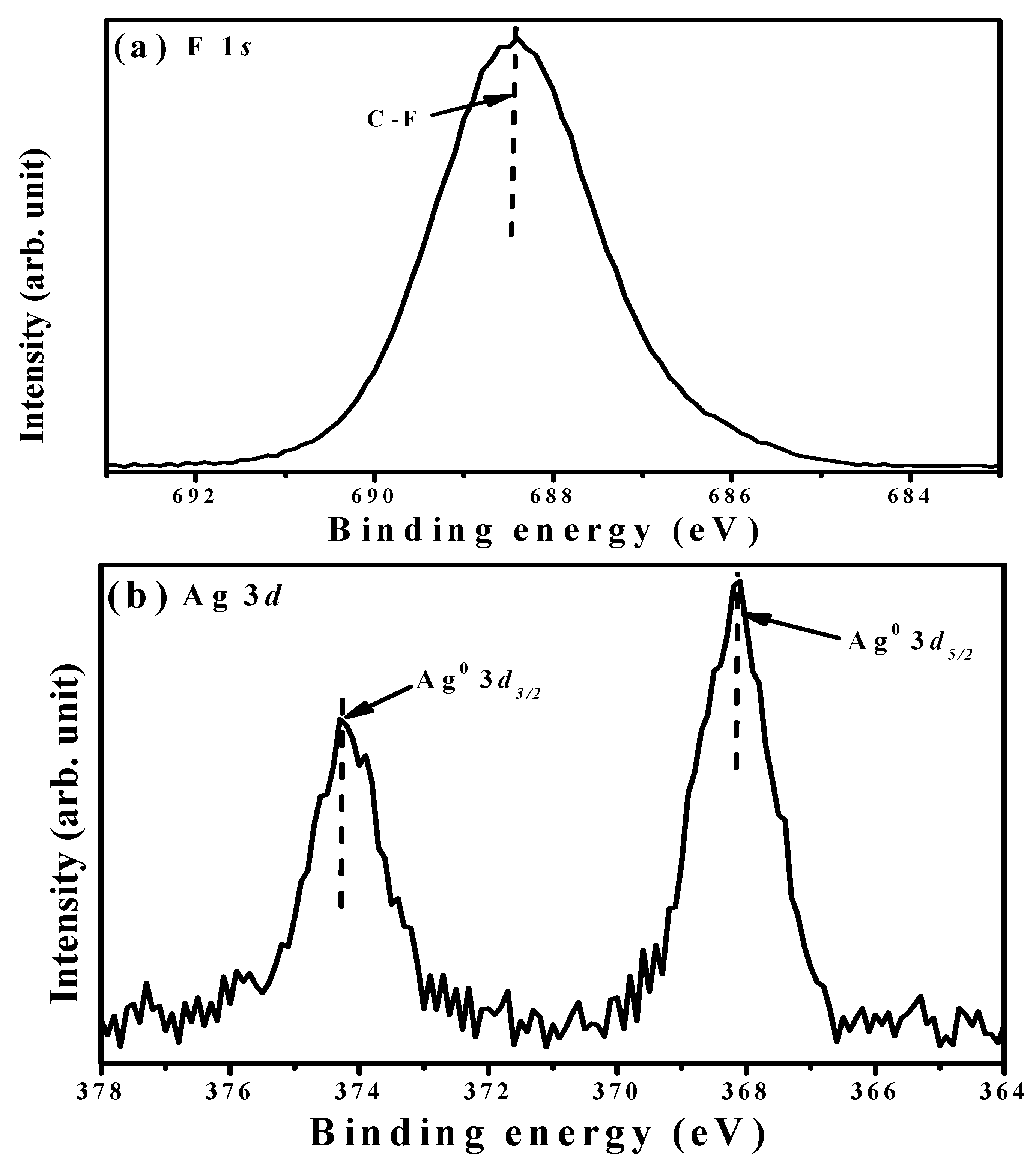
3. Results and Discussion
4. Conclusions
Author Contributions
Funding
Conflicts of Interest
References
- Uhlmann, P.; Frenzel, R.; Voit, B.; Mock, U.; Szyszka, B.; Schmidt, B.; Ondratschek, D.; Gochermann, J.; Roths, K. Research agenda surface technology: Future demands for research in the field of coatings materials. Prog. Org. Coat. 2007, 58, 122–126. [Google Scholar] [CrossRef]
- Wu, L.Y.L.; Nigian, S.K.; Chen, Z.; Xuan, D.T.T. Quantitative test method for evaluation of anti-fingerprint property of coated surface. Appl. Surf. Sci. 2011, 257, 2965–2969. [Google Scholar] [CrossRef]
- Yin, L.; Yang, J.; Tang, Y.; Chen, L.; Liu, C.; Tang, H.; Li, C. Mechanical durability of superhydrophobic and oleophobic copper meshes. Appl. Surf. Sci. 2014, 316, 259–263. [Google Scholar] [CrossRef]
- Li, H.; Wang, J.; Yang, L.; Song, Y. Superoleophilic and superhydrophobic inverse opals for oil sensors. Adv. Funct. Mater. 2008, 18, 3258–3264. [Google Scholar] [CrossRef]
- Huang, Y.; Zhou, J.; Su, B.; Shi, L.; Wang, J.; Chen, S.; Wang, L.; Zi, J.; Song, Y.; Jiang, L. Collodial Photonic Crystals with narrow stopbands assembled from low-adhesive superhydrophobic substrates. J. Am. Chem. Soc. 2012, 134, 17053–17058. [Google Scholar] [CrossRef] [PubMed]
- Owen, M.J. Silicone hydrophobocity and oleophilicity. Silicon 2017, 9, 651–655. [Google Scholar] [CrossRef]
- Kwok, D.Y.; Neumann, A.W. Contact angle measurement and contact angle interpretation. Adv. Colloid Interface Sci. 1999, 81, 167–249. [Google Scholar] [CrossRef]
- Zhu, L.; Hao, G.; Chen, Y.; Chen, Y. Investigation on hydrophobic film from a hydrophobic powder. Appl. Surf. Sci. 2012, 261, 863–867. [Google Scholar] [CrossRef]
- Xu, K.; Hu, J.; Jiang, X.; Meng, W.; Lan, B.; Shu, L. Anti-icing performance of hydrophobic silicone-acrylate resin coatings on wind blades. Materials 2018, 8, 15. [Google Scholar] [CrossRef]
- Kujawa, J.; Al-Gharabli, S.; Kujawski, W.; Knozowska, K. Molecular grafting of fluorinated and nanofluorinated Alkylsiloxanes on various ceramic membrane surface for the removal of volatile organic compounds applying vacuum membrane distillation. ACS Appl. Mater. Interface 2017, 9, 6571–6590. [Google Scholar] [CrossRef] [PubMed]
- Al-Gharabli, S.; Hamad, E.; Saket, M.; El-Rub, Z.A.; Arafat, H.; Kujawski, W.; Kujawa, J. Advanced material-ordered nanotubular ceramic membranes covalently capped with single-wall carbon nanotubes. Materials 2018, 11, 739. [Google Scholar] [CrossRef] [PubMed]
- Wu, C.Y.; Chen, W.C.; Liu, D.S. Surface modification layer deposition on flexibility substrates by plasma-enhanced chemical vapour deposition using tertamethylsilane-oxygen gas mixture. J. Phys. D Appl. Phys. 2008, 41, 225305. [Google Scholar] [CrossRef]
- Liu, D.S.; Wu, C.Y. Adhesion enhancement of hard coatings deposited on flexible plastic substrates using an interfacial buffer layer. J. Phys. D Appl. Phys. 2010, 43, 175301. [Google Scholar] [CrossRef]
- Öner, D.; McCarthy, T.J. Ultrahydrophobic surface. Effects of topography length scales on wettability. Langmuir 2000, 16, 7777–7782. [Google Scholar] [CrossRef]
- Shirtcliffe, N.J.; Mchale, G.; Newton, M.I.; Perry, C.C. Intrinsically superhydrophobic organosilica sol-gel foams. Langmir 2003, 19, 5626–5631. [Google Scholar] [CrossRef]
- Koch, K.; Bhushan, B.; Barthlott, W. Multifunctional surface structures of plants: An inspiration for biomimetics. Prog. Mater. Sci. 2009, 54, 137–178. [Google Scholar] [CrossRef]
- Hsieh, C.T.; Wu, F.L.; Chen, W.Y. Super water- and oil-repellences form silica-based nanocoatings. Surf. Coat. Technol. 2009, 203, 3377–3384. [Google Scholar] [CrossRef]
- Cansoy, C.E.; Erbil, H.Y.; Akar, O.; Akin, T. Effect of pattern size and geometry on the use of Cassie-Baxter equation for superhydrophobic surfaces. Colloid Surf. A-Physicochem. Eng. Asp. 2011, 386, 116–124. [Google Scholar] [CrossRef]
- Tian, D.; Song, Y.; Jiang, L. Patterning of controllable surface wettability for printing techniques. Chem. Soc. Rev. 2013, 42, 5184–5209. [Google Scholar] [CrossRef] [PubMed]
- Hsieh, C.T.; Chen, J.M.; Kuo, R.R.; Lin, T.S.; Wu, C.F. Influence of surface roughness on water- and oil-repellent surfaces coated with nanoparticles. Appl. Surf. Sci. 2005, 240, 318–326. [Google Scholar] [CrossRef]
- Basu, B.J.; Kumar, V.D.; Anandan, C. Surface studies on superhydrophobic and oleophobic polydimethylsiloxane–silica nanocomposite coating system. Appl. Surf. Sci. 2012, 261, 807–814. [Google Scholar] [CrossRef]
- Aminayi, P.; Abidi, N. Ultra-oleophobic cotton fabric prepared using molecular and nanoparticle vapor deposition methods. Surf. Coat. Technol. 2015, 276, 636–644. [Google Scholar] [CrossRef]
- Durrent, J.; Frolet, N.; Gourgon, C. Hydrophobicity and anti-icing performances of nanoimprinted and roughened fluoropolymers film under overcooled temperature. Microelectron. Eng. 2016, 155, 1–6. [Google Scholar] [CrossRef]
- Gingery, D.; Bühlmann, P. Formation of gold nanoparticles on multiwalled carbon nanotubes by thermal evaporation. Carbon 2008, 46, 1966–1972. [Google Scholar] [CrossRef]
- Franc, J.; Bastl, Z. Nickel evaporation in high vacuum and formation of nickel oxide nanoparticles on highly oriented pyrolytic graphite. X-ray photoelectron spectroscopy an atomic force microscopy study. Thin Solid Films 2008, 516, 6095–6103. [Google Scholar] [CrossRef]
- Abou El-Nour, K.M.M.; Eftaiha, A.; Al-Warthan, A.; Ammar, R.A.A. Synthesis and applications of silver nanoparticles. Arab. J. Chem. 2010, 3, 135–140. [Google Scholar] [CrossRef]
- Gromov, D.G.; Pavlova, L.M.; Savitsky, A.I.; Yu, T.A. Nucleation and growth of Ag nanoparticles on amorphous carbon surface from vapor phase formed by vacuum evaporation. Appl. Phys. A 2015, 118, 1297–1303. [Google Scholar] [CrossRef]
- Kang, C.Y.; Chao, C.H.; Shiu, S.C. Formation of self-organized platinum nanoparticles and their microphotoluminescence enhancement in the visible light region. J. Appl. Phys. 2007, 102, 073508. [Google Scholar] [CrossRef]
- Schmiitt, J.; Hajiw, S.; Lecchi, A.; Degrouard, J.; Salonen, A.; Impéror-Clerc, M.; Pansu, B. Formation of superlattices of gold nanoparticles using Ostwald ripening in emulsions: transition for fcc to bcc structure. J. Phys. Chem. B 2016, 120, 5759–5766. [Google Scholar] [CrossRef] [PubMed]
- Igathinathane, C.; Pordesimo, L.O.; Columbus, E.P.; Batchelor, W.D.; Methuku, S.R. Shape identification and particles size distribution from basic shape parameters using Image. J. Comput. Electron. Agric. 2008, 63, 168–182. [Google Scholar] [CrossRef]
- Maier, S.A.; Atwater, H.A. Plasmonics: Localization and guiding of electromagnetic energy in metal/dielectric structures. J. Appl. Phys. 2005, 98, 011101. [Google Scholar] [CrossRef] [Green Version]
- Willets, K.A.; Wan Duyne, R.P. Localized surface plasmon resonance spectroscopy and sensing. Annu. Rev. Phys. Chem. 2007, 58, 267–297. [Google Scholar] [CrossRef] [PubMed]
- Xu, W.F.; Chin, C.C.; Hung, D.W.; Wei, P.K. Transparent electrode for organic solar cells using multilayer structures with nanoporous silver film. Sol. Energy Mater. Sol. Cells 2013, 118, 81–89. [Google Scholar] [CrossRef]
- Zhang, S.G.; Zhang, X.W.; Yin, Z.G.; Wang, J.X.; Si, F.T.; Gao, H.L.; Dong, J.J.; Liu, X. Optimization of electroluminescence from n-ZnO/AlN/p-GaN light-emitting diodes by tailoring Ag localizer surface plasmon. J. Appl. Phys. 2012, 112, 013112. [Google Scholar] [CrossRef]
- Mogensen, K.B.; Kneipp, K. Size-dependent shifts of plasmon resonance in silver nanoparticle films using controlled dissolution: Monitoring the onset of the surface screening effects. J. Phys. Chem. C 2014, 118, 28075–28083. [Google Scholar] [CrossRef]
- Wenzel, R.N. Resistance of solid surface to wetting by water. Ind. Eng. Chem. 1936, 28, 988–994. [Google Scholar] [CrossRef]
- Hong, B.S.; Han, J.H.; Kim, S.T.; Cho, Y.J.; Park, M.S.; Dolukhanyan, T.; Sung, C. Endurable water-repellent glass for automobiles. Thin Solid Films 1999, 351, 274–278. [Google Scholar] [CrossRef]
- Tan, I.H.; da Silva, M.L.P.; Demarquette, N.R. Paper surface modification by plasma deposition of double layers of organic silicon compounds. J. Mater. Chem. 2001, 11, 1019–1025. [Google Scholar] [CrossRef]
- Teshima, K.; Sugimura, H.; Inoue, Y.; Takai, O. Gas barrier performance of surface-modified silica films with grafted organosilane molecules. Langmuir 2003, 19, 8331–8334. [Google Scholar] [CrossRef]
- Kim, J.D.; Lee, K.Y.; Kim, K.Y.; Sugimura, H.; Takai, O.; Wu, Y.; Inoue, Y. Characteristics and high water-repellency of a-C:H films deposited by r.f. PECVD. Surf. Coat. Technol. 2003, 162, 135–139. [Google Scholar] [CrossRef]
- Wu, C.Y.; Liao, R.M.; Lai, L.W.; Jeng, M.S.; Liu, D.S. Organosilicon/silicon oxide gas barrier structure encapsulated flexible plastic substrate by using plasma-enhanced chemical vapor deposition. Surf. Coat. Technol. 2012, 206, 4685–4691. [Google Scholar] [CrossRef]
- Nakagawa, T.; Hiwatashi, T. Water-repellent thin films from mixtures of fluoroalkylmethoxysilane and bis-(trialkoxysilyl)alkanes of various carbon-chain lengths using the sol–gel method and the fluoroalkylmethoxysilane dispersion mechanism. J. Non-Cryst. Solids 2003, 316, 228–237. [Google Scholar] [CrossRef]
- Kang, G.S.; Ko, H.J.; Choi, C.K. Chemical bond structure of a-C:F films with a low dielectric constant deposited by using CH4/CF4 ICPCVD. J. Korean Phys. Soc. 2003, 42, 676–681. [Google Scholar]
- Chen, G.; Zhang, J.; Yang, S. Fabrication of hydrophobic fluorinated amorphous carbon thin films by an electrochemical route. Electrochem. Commun. 2008, 10, 7–11. [Google Scholar] [CrossRef]
- Choi, W.K.; Ong, T.Y.; Tan, L.S.; Loh, F.C.; Tan, K.L. Infrared and x-ray photoelectron spectroscopy studies of as-prepared and furnace-annealed radio-frequency sputtered amorphous silicon carbide films. J. Appl. Phys. 1998, 83, 4968–4973. [Google Scholar] [CrossRef]
- Brinkmann, M.; Chan, V.Z.H.; Thomas, E.L.; Lee, V.Y.; Miller, D.; Hadjichristidis, N.; Avgeropoulos, A. Room-temperature synthesis of a-SiO2 thin films by UV-assisted ozonolysis of a polymer precursor. Chem. Mater. 2001, 13, 967–972. [Google Scholar] [CrossRef]
- Trey, S.M.; Sidenvall, P.; Alavi, K.; Ståhlberg, D.; Johansson, M. Dual cure (UV/thermal) primers for composite substrates—Effect of surface treatment and primer composition on adhesion. Prog. Org. Coat. 2009, 64, 489–496. [Google Scholar] [CrossRef]
- Khung, Y.L.; Nghlim, S.H.; Meda, L.; Narducci, D. Preferential formation of Si-O-C over Si-C linkage upon thermal grafting on hydrogen-terminated silicon (111). Chemistry 2014, 20, 15151–15158. [Google Scholar] [CrossRef] [PubMed]
- David, L.; Bhandavat, R.; Barrera, U.; Singh, G. Silicon oxycarbide glass-graphene composite paper electrode for long cycle lithium-ion batteries. Nat. Commun. 2016, 7, 10998. [Google Scholar] [CrossRef] [PubMed]
- Ferraria, A.M.; da Silva, J.D.L.; do Rego, A.M.B. XPS studied of directly fluorinated HDPE: Problem and solution. Polymer 2003, 44, 7241–7249. [Google Scholar] [CrossRef]
- Wang, C.; Lai, P.C.; Syu, S.H.; Leu, J. Effects of CF4 plasma treatment on the moisture uptake, diffusion, and WVTR of poly(ethylene terephthalate) flexible films. Surf. Coat. Technol. 2011, 206, 318–324. [Google Scholar] [CrossRef]
- Lakshmi, R.V.; Bharathidasan, T.; Bera, P.; Basu, B.J. Fabrication of superhydrophobic and oleophobic sol–gel nanocomposite coating. Surf. Coat. Technol. 2012, 206, 3888–3894. [Google Scholar] [CrossRef]
- True, J.E.; Thomas, T.D.; Winter, R.W.; Gard, G.L. Electronegativities from core-ionization energies: Electronegativities of SF5 and CF3. Inorg. Chem. 2003, 42, 4437–4441. [Google Scholar] [CrossRef] [PubMed]
- Dai, Y.; Cai, S.; Wu, L.; Yang, W.; Xie, J.; Wen, W.; Zheng, J.C.; Zhu, Y. Surface modified CFx cathode material for ultrafast discharge and high energy density. J. Mater. Chem. A 2014, 2, 20896–20901. [Google Scholar] [CrossRef]
- Li, Y.; Veith, G.M.; Browning, K.I.; Chen, J.; Hensley, D.K.; Paranthaman, M.P.; Dai, S.; Sun, X.G. Lithium malonatoborate additives enabled stable cycling of 5 V lithium metal and lithium ion batteries. Nano Energy 2017, 40, 9–19. [Google Scholar] [CrossRef]
- Ma, J.; Guo, X.; Zhang, Y.; Ge, H. Catalytic performance of TiO2@Ag composites prepared by modified photodeposition method. Chem. Eng. J. 2014, 258, 247–253. [Google Scholar] [CrossRef]
- Liu, F.C.; Li, J.Y.; Chen, T.H.; Chang, C.H.; Lee, C.T.; Hsiao, W.H.; Liu, D.S. Effect of Silver Dopants on the ZnO Thin Films Prepared by a Radio Frequency Magnetron Co-Sputtering System. Materials 2017, 10, 797–808. [Google Scholar] [CrossRef] [PubMed]


| Sample | Ag Deposition Time (s) | ||||
|---|---|---|---|---|---|
| Parameter | 75 | 150 | 480 | 720 | |
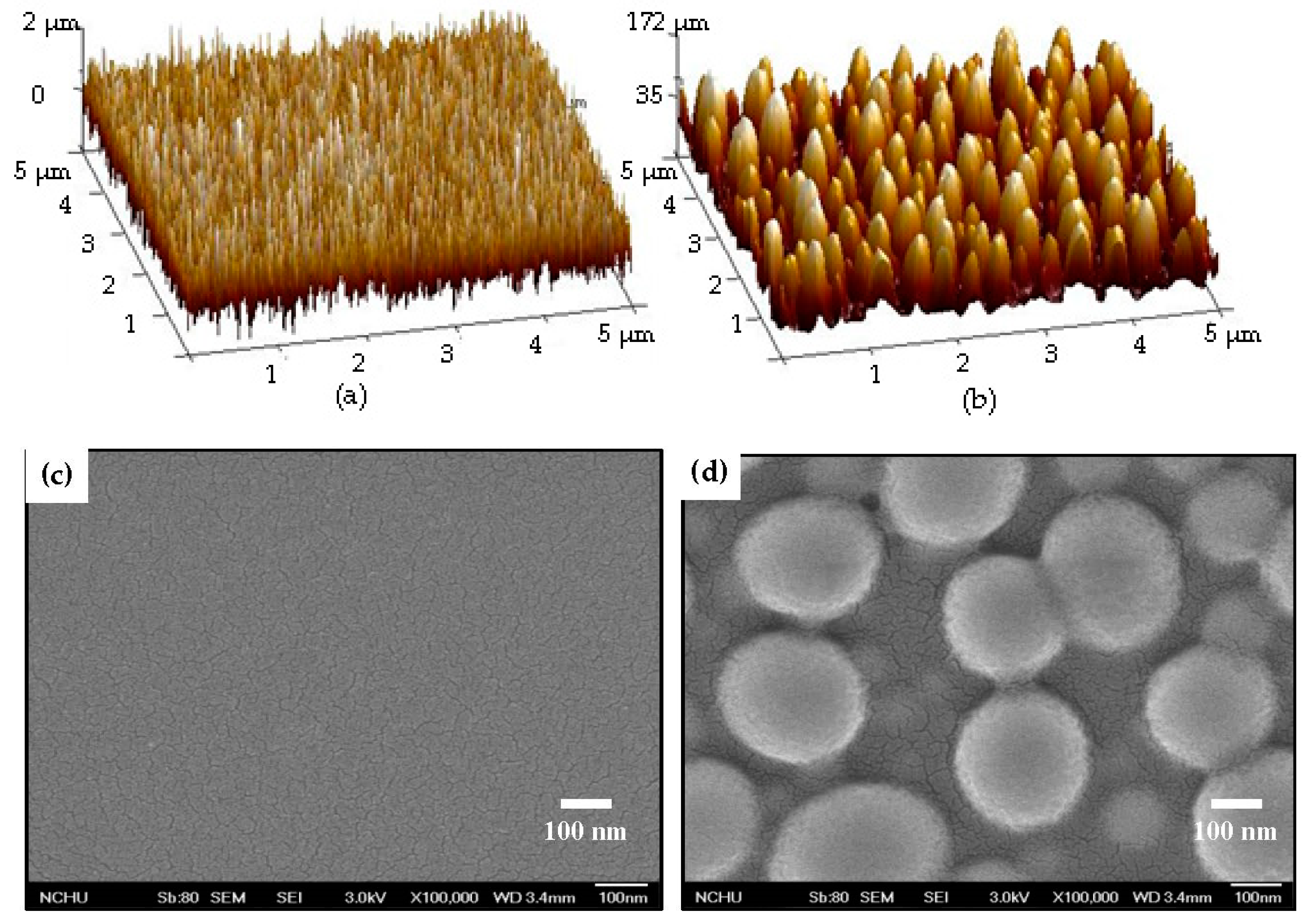
| Rq (nm) | 18.2 | 31.6 | 52.8 | 76.0 | |
| Mean particle size (nm) | 72 ± 44 | 84 ± 66 | 181 ± 97 | 232 ± 138 | |
| Tavg (%) | 86 | 82 | 35 | 46 | |
| Surface coverage (%) | 20.4 | 22.9 | 41.3 | 28.1 | |
| Absorbance peak (nm) | 411 | 417 | 437 | 438 | |
| Sample | Rq (nm) | WCA (°) | OCA (°) |
|---|---|---|---|
| Organosilicon on silicon substrate | 0.4 | 100 ± 0.2 | 11 ± 1.1 |
| Organosilicon on as-deposited Ag seed layer | 1.9 | 103 ± 0.6 | 10 ± 0.4 |
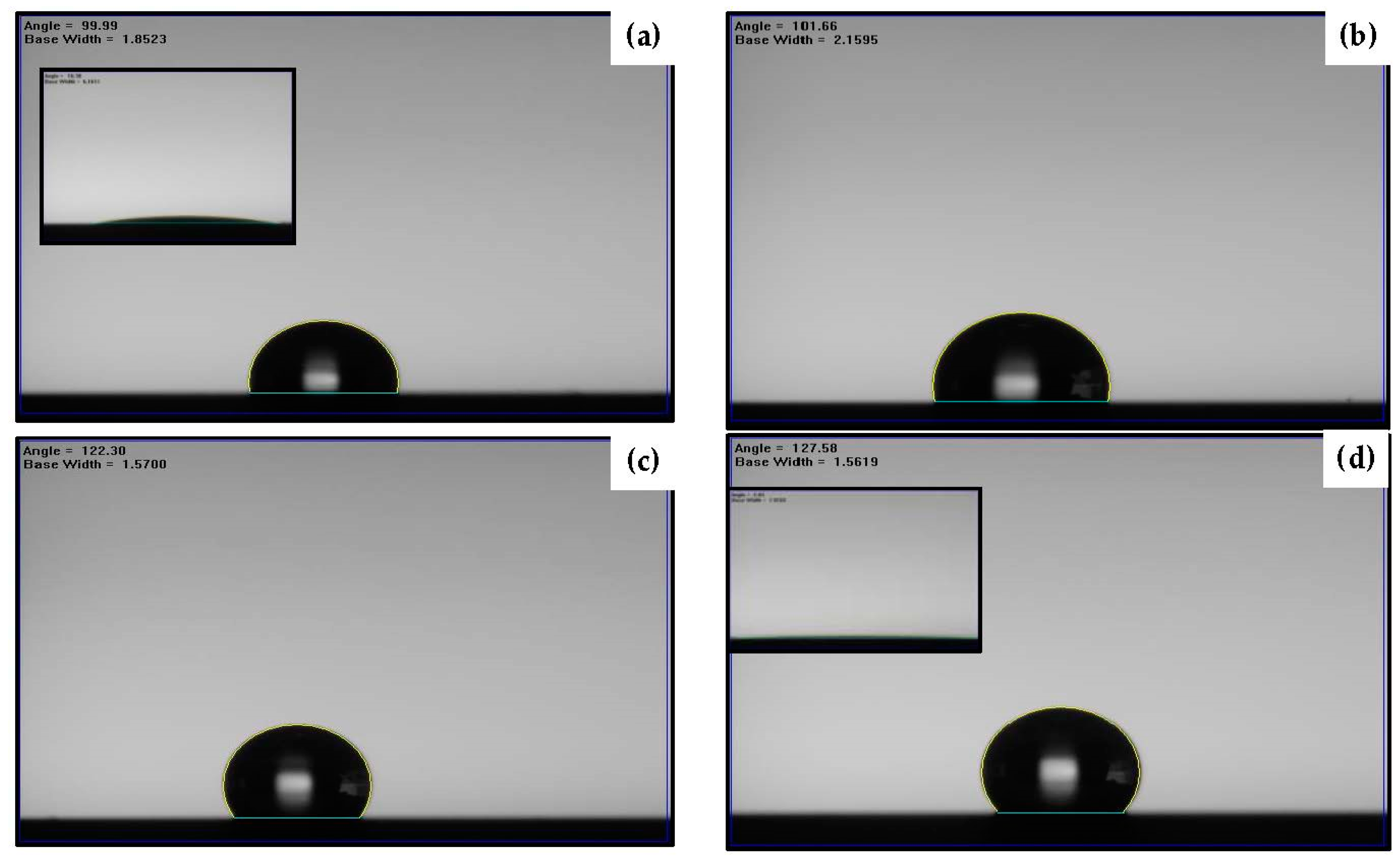
| Organosilicon on annealed Ag seed layer (150 s) | 18.1 | 122 ± 0.5 | 7 ± 0.5 |
| Organosilicon on annealed Ag seed layer (480 s) | 49.8 | 128 ± 0.8 | 3 ± 0.3 |
| Sample | CF4 Plasma Etching Time (s) | |||||
|---|---|---|---|---|---|---|
| 0 | 15 | 30 | 40 | 60 | ||
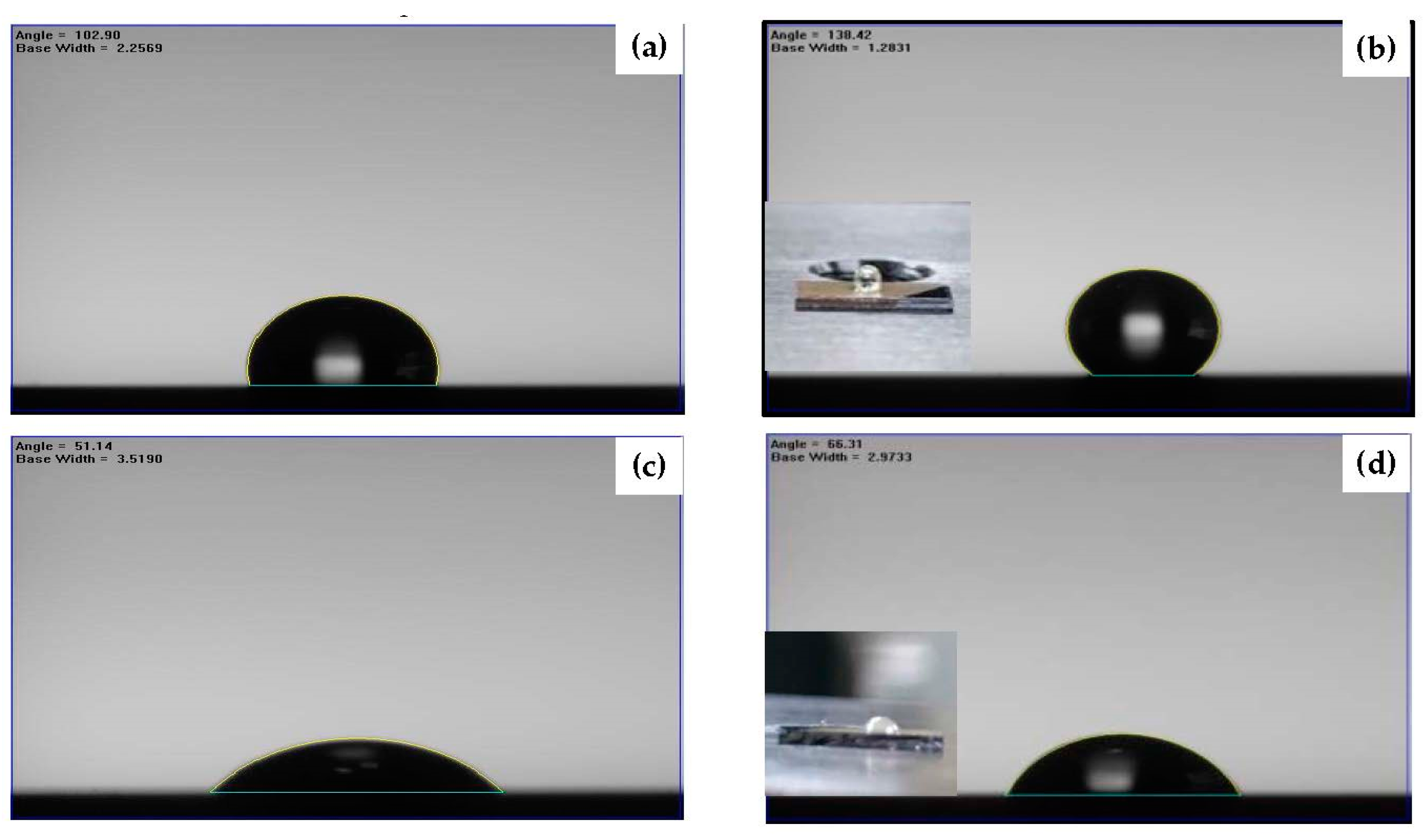
| Organosilicon on silicon substrate | WCA (o) | 100 ± 0.2 | 104 ± 0.3 | 103 ± 0.2 | 103 ± 0.3 | 103 ± 0.4 |
| OCA (o) | 11 ± 1.1 | 50 ± 1.4 | 51 ± 1.0 | 51 ± 1.6 | 50 ± 0.8 | |
| Organosilicon on annealed Ag seed layer | WCA (o) | 128 ± 0.8 | 132 ± 0.9 | 135 ± 0.8 | 138 ± 0.6 | 70 ± 0.7 |
| OCA (o) | 3 ± 0.3 | 60 ± 0.6 | 62 ± 0.9 | 66 ± 0.7 | 7 ± 0.2 | |
© 2018 by the authors. Licensee MDPI, Basel, Switzerland. This article is an open access article distributed under the terms and conditions of the Creative Commons Attribution (CC BY) license (http://creativecommons.org/licenses/by/4.0/).
Share and Cite
Xu, Z.-W.; Zhang, Y.-K.; Chen, T.-H.; Chang, J.-H.; Lee, T.-H.; Li, P.-Y.; Liu, D.-S. Enhancement on the Surface Hydrophobicity and Oleophobicity of an Organosilicon Film by Conformity Deposition and Surface Fluorination Etching. Materials 2018, 11, 1089. https://doi.org/10.3390/ma11071089
Xu Z-W, Zhang Y-K, Chen T-H, Chang J-H, Lee T-H, Li P-Y, Liu D-S. Enhancement on the Surface Hydrophobicity and Oleophobicity of an Organosilicon Film by Conformity Deposition and Surface Fluorination Etching. Materials. 2018; 11(7):1089. https://doi.org/10.3390/ma11071089
Chicago/Turabian StyleXu, Zheng-Wen, Yu-Kai Zhang, Tai-Hong Chen, Jin-How Chang, Tsung-Hsin Lee, Pei-Yu Li, and Day-Shan Liu. 2018. "Enhancement on the Surface Hydrophobicity and Oleophobicity of an Organosilicon Film by Conformity Deposition and Surface Fluorination Etching" Materials 11, no. 7: 1089. https://doi.org/10.3390/ma11071089