Thickness Characterization Toolbox for Transparent Protective Coatings on Polymer Substrates

 ,
,  ,
,  ,
, 
Abstract
:1. Introduction
2. Materials and Methods
3. Results and Discussion
3.1. Precursor Synthesis and Deposition
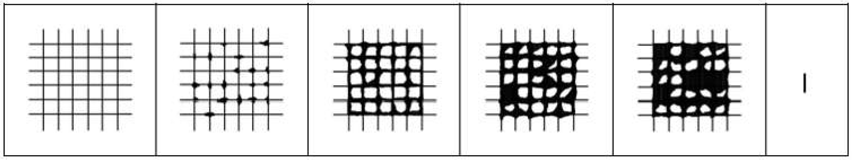
3.2. Layer Thickness Determination
3.3. Window Film Characteristics
3.3.1. Application Tests
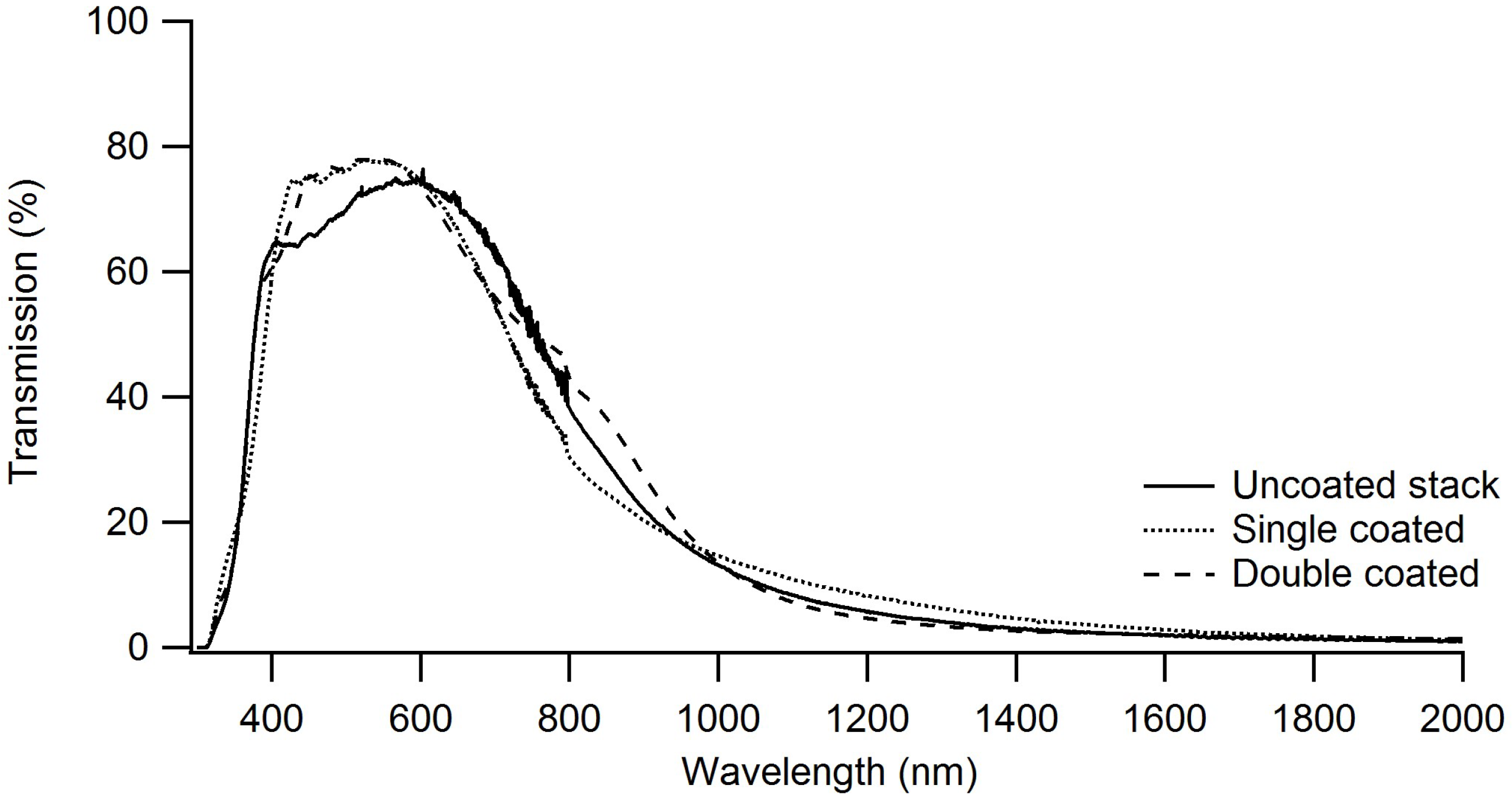
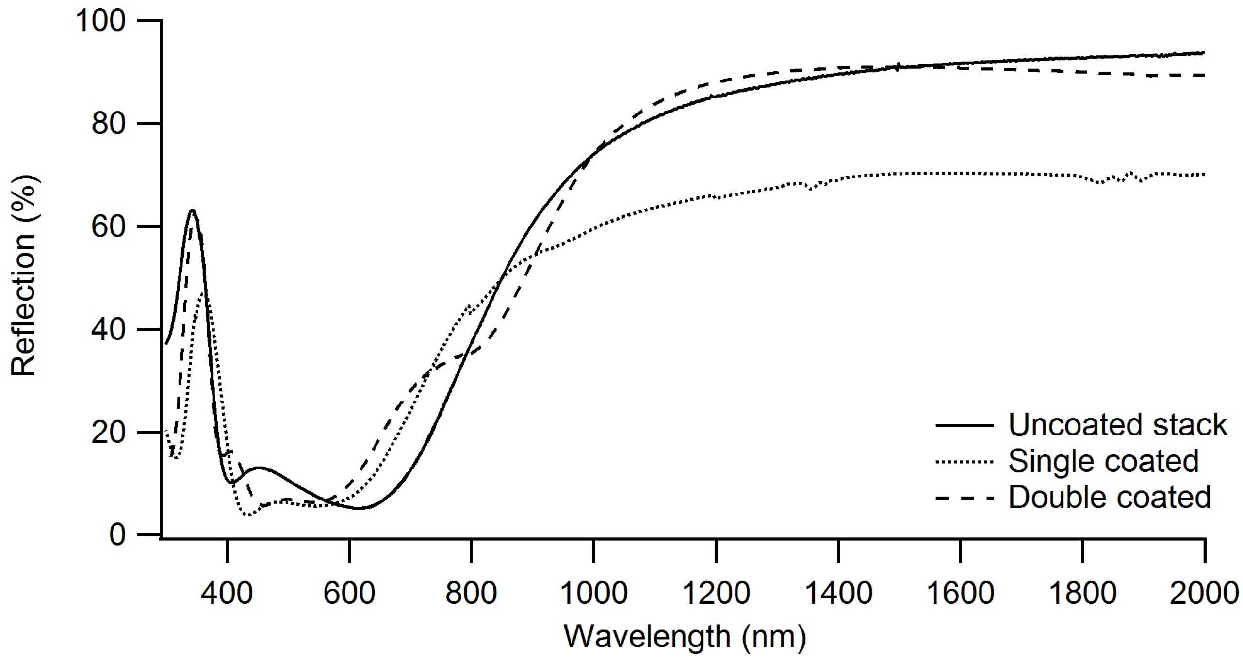
3.3.2. Visual Transmission and Infrared Reflection Properties
4. Conclusions
5. Patents
Author Contributions
Funding
Acknowledgments
Conflicts of Interest
References
- Fan, J.C.C.; Bachner, F.J.; Foley, G.H.; Zavracky, P.M. Transparent heat-mirror films of TiO2/Ag/TiO2 for solar energy collection and radiation insulation. Appl. Phys. Lett. 1974, 25, 693–695. [Google Scholar] [CrossRef]
- Ando, E.; Miyazaki, M. Moisture degradation mechanism of silver-based low-emissivity coatings. Thin Solid Films 1999, 351, 308–312. [Google Scholar] [CrossRef]
- Ando, E.; Miyazaki, M. Moisture resistance of the low-emissivity coatings with a layer structure of Al-doped ZnO/Ag/Al-doped ZnO. Thin Solid Films 2001, 392, 289–293. [Google Scholar] [CrossRef]
- Ando, E.; Suzuki, S.; Aomine, N.; Miyazaki, M.; Tada, M. Sputtered silver-based low-emissivity coatings with high moisture durability. Vacuum 2000, 59, 792–799. [Google Scholar] [CrossRef]
- Miyazaki, M.; Ando, E. Durability improvement of Ag-based low-emissivity coatings. J. Non-Cryst. Solids 1994, 178, 245–249. [Google Scholar] [CrossRef]
- Ross, R. Observations on humidity-induced degradation of Ag-based low-emissivity films. Solar Energy Mater. 1990, 21, 25–42. [Google Scholar] [CrossRef]
- Nadel, S.J. Durability of Ag based low-emissivity coatings. J. Vac. Sci. Technol. A 1987, 5, 2709–2713. [Google Scholar] [CrossRef]
- Vernieuwe, K.; Cuypers, D.; Kirschhock, C.E.A.; Houthoofd, K.; Vrielinck, H.; Lauwaert, J.; De Roo, J.; Martins, J.C.; Van Driessche, I.; De Buysser, K. Thermal processing of aqueous AZO inks towards functional TCO thin films. J. Alloys Compd. 2017, 690, 360–368. [Google Scholar] [CrossRef]
- Levine, J.B.; Ciraldo, J.P. Method of Growing Aluminum Oxide onto Substrates by Use of an Aluminum Source in an Environment Containing Partial Pressure of Oxygen to Create Transparent, Scratch-Resistant Windows. U.S. Patent US2016215381 (A1), 28 July 2016. [Google Scholar]
- Sangermano, M.; Perrot, A.; Gigot, A.; Rivolo, P.; Pirri, F.; Messori, M. Hydrophobic Scratch Resistant UV-Cured Epoxy Coating. Macromol. Mater. Eng. 2016, 301, 93–98. [Google Scholar] [CrossRef]
- Groenewolt, M.; Kues, J.B.; Schroeder, S.; Cavaleiro, P.; Karminski, H.L.; Michael, G. High-Transparency Polycarbonates with Scratch-Resistant Coating, Process for Production Thereof and Use Thereof. U.S. Patent US200913129528, 28 October 2014. [Google Scholar]
- Amerio, E.; Fabbri, P.; Malucelli, G.; Messori, M.; Sangermano, M.; Taurino, R. Scratch resistance of nano-silica reinforced acrylic coatings. Prog. Org. Coat. 2008, 62, 129–133. [Google Scholar] [CrossRef]
- Tahmassebi, N.; Moradian, S.; Ramezanzadeh, B.; Khosravi, A.; Behdad, S. Effect of addition of hydrophobic nano silica on viscoelastic properties and scratch resistance of an acrylic/melamine automotive clearcoat. Tribol. Int. 2010, 43, 685–693. [Google Scholar] [CrossRef]
- Kues, J.B.; Brosseit, A.; Homann, K.; Schroeder, S. Plastic Substrates Having a Scratch-Resistant Coating, in Particular Housings of Electronic Devices, Having High Transparency, Method for the Production Thereof, and Use Thereof. U.S. Patent US201013577100, 28 April 2015. [Google Scholar]
- Watté, J.; Van Zele, M.; De Buysser, K.; Van Driessche, I. Recent Advances in Low-Temperature Deposition Methods of Transparent, Photocatalytic TiO2 Coatings on Polymers. Coatings 2018, 8, 131. [Google Scholar] [CrossRef]
- Rijckaert, H.; Pollefeyt, G.; Sieger, M.; Hänisch, J.; Bennewitz, J.; De Keukeleere, K.; De Roo, J.; Hühne, R.; Bäcker, M.; Paturi, P.; et al. Optimizing Nanocomposites through Nanocrystal Surface Chemistry: Superconducting YBa2Cu3O7 Thin Films via Low-Fluorine Metal Organic Deposition and Preformed Metal Oxide Nanocrystals. Chem. Mater. 2017, 29, 6104–6113. [Google Scholar] [CrossRef]
- Narayanan, V.; Lommens, P.; De Buysser, K.; Vanpoucke, D.E.P.; Huehne, R.; Molina, L.; Van Tendeloo, G.; Van Der Voort, P.; Van Driessche, I. Aqueous CSD approach for the growth of novel, lattice-tuned LaxCe1−xOδ epitaxial layers. J. Mater. Chem. 2012, 22, 8476. [Google Scholar] [CrossRef]
- Pollefeyt, G.; Clerick, S.; Vermeir, P.; Lommens, P.; De Buysser, K.; Van Driessche, I. Influence of Aqueous Precursor Chemistry on the Growth Process of Epitaxial SrTiO3 Buffer Layers. Inorg. Chem. 2014, 53, 4913–4921. [Google Scholar] [CrossRef] [PubMed]
- Pollefeyt, G.; Rottiers, S.; Vermeir, P.; Lommens, P.; Hühne, R.; De Buysser, K.; Van Driessche, I. Feasibility study of the synthesis of YBiO3 thin films by aqueous chemical solution deposition as an alternative for CeO2 buffer layers in coated conductors. J. Mater. Chem. A 2013, 1, 3613–3619. [Google Scholar] [CrossRef]
- ASTM D3359-09e2. Standard Test Methods for Measuring Adhesion by Tape Test; ASTM International: West Conshohocken, PA, USA, 2009. [Google Scholar]
- ASTM D3363-05(2011)e2. Standard Test Method for Film Hardness by Pencil Test; ASTM International: West Conshohocken, PA, USA, 2011. [Google Scholar]
- Yasuda, M.; Morimoto, K.; Kainuma, Y.; Kawata, H.; Hirai, Y. Analysis of Charging Phenomena of Polymer Films on Silicon Substrates under Electron Beam Irradiation. Jpn. J. Appl. Phys. 2008, 47, 4890–4892. [Google Scholar] [CrossRef]
- Geltmeyer, J.; De Roo, J.; Van den Broeck, F.; Martins, J.C.; De Buysser, K.; De Clerck, K. The influence of tetraethoxysilane sol preparation on the electrospinning of silica nanofibers. J. Sol-Gel Sci. Technol. 2016, 77, 453–462. [Google Scholar] [CrossRef]
- Geltmeyer, J.; Van der Schueren, L.; Goethals, F.; De Buysser, K.; De Clerck, K. Optimum sol viscosity for stable electrospinning of silica nanofibres. J. Sol-Gel Sci. Technol. 2013, 67, 188–195. [Google Scholar] [CrossRef] [Green Version]
- Goethals, F.; Ciofi, I.; Madia, O.; Vanstreels, K.; Baklanov, M.R.; Detavernier, C.; Van Der Voort, P.; Van Driessche, I. Ultra-low-k cyclic carbon-bridged PMO films with a high chemical resistance. J. Mater. Chem. 2012, 22, 8281–8286. [Google Scholar] [CrossRef]
- De Buysser, K.; Ide, M.; Van Zele, M.; Van Driessche, I. A Method of Manufacturing a Coated Polymer Substrate Having Low Emissivity. WO2016EP79943, 6 December 2016. [Google Scholar]
- Caillot, M.; Chaumonnot, A.; Digne, M.; Poleunis, C.; Debecker, D.P.; van Bokhoven, J.A. Synthesis of amorphous aluminosilicates by grafting: Tuning the building and final structure of the deposit by selecting the appropriate synthesis conditions. Microporous Mesoporous Mater. 2014, 185, 179–189. [Google Scholar] [CrossRef]
- De Ferri, L.; Lorenzi, A.; Lottici, P.P. OctTES/TEOS system for hybrid coatings: Real-time monitoring of the hydrolysis and condensation by Raman spectroscopy. J. Raman Spectrosc. 2016, 47, 699–705. [Google Scholar] [CrossRef]
- Matos, M.C.; Ilharco, L.M.; Almeida, R.M. The evolution of TEOS to silica gel and glass by vibrational spectroscopy. J. Non-Cryst. Solids 1992, 147–148, 232–237. [Google Scholar] [CrossRef]
- Depla, A.; Lesthaeghe, D.; van Erp, T.S.; Aerts, A.; Houthoofd, K.; Fan, F.; Li, C.; Van Speybroeck, V.; Waroquier, M.; Kirschhock, C.E.A.; et al. 29Si NMR and UV−Raman Investigation of Initial Oligomerization Reaction Pathways in Acid-Catalyzed Silica Sol−Gel Chemistry. J. Phys. Chem. C 2011, 115, 3562–3571. [Google Scholar] [CrossRef]
- Devreux, F.; Boilot, J.; Chaput, F.; Lecomte, A. Sol-gel condensation of rapidly hydrolyzed silicon alkoxides: A joint Si 29 NMR and small-angle X-ray scattering study. Phys. Rev. A 1990, 41, 6901–6909. [Google Scholar] [CrossRef] [PubMed]
- Turner, C.W.; Franklin, K.J. Studies of the hydrolysis and condensation of tetraethylorthosilicate by multinuclear (1H, 17O, 29Si) nmr spectroscopy. J. Non-Cryst. Solids 1987, 91, 402–415. [Google Scholar] [CrossRef]


| Parameter | Setting |
|---|---|
| Unwinding speed | 2.4 m/min |
| Application speed | 1 m/min |
| Coating method | Reverse gravure |
| Temperature first oven | 60 °C |
| Temperature second oven | 80 °C |
| Band Profile | Description |
|---|---|
| Monomer | Height to zero, peak from 665 to 645nm |
| Dimer and end group | Height to zero, peak from 605 to 585 nm, referenced to monomer |
| Trimer | Height to zero, peak from 580 to 560 nm, referenced to monomer |
| Tetramer | Height to zero, peak from 560 to 540 nm, referenced to monomer |
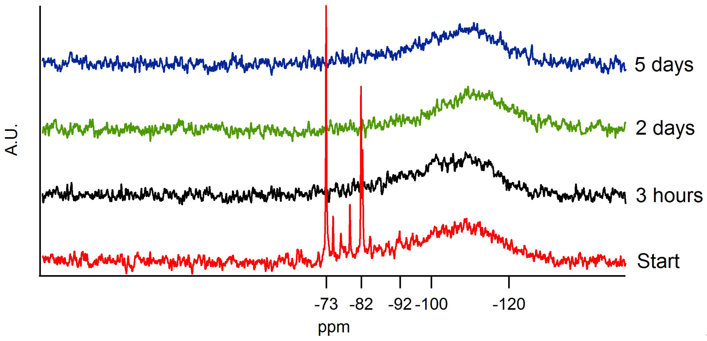
| Label | δ ppm | Silicate Structure |
|---|---|---|
| Q0hydrolized | −73 | Si*(OH)4 |
| Q0 | −82 | Si*(OR)4 |
| Q2 | −92 | Si*(OR)3(−O−Si≡) |
| Q3 and Q4 | −100 to −120 | Si*(OR)2(−O−Si≡)2 Si*(OR)(−O−Si≡)3 |
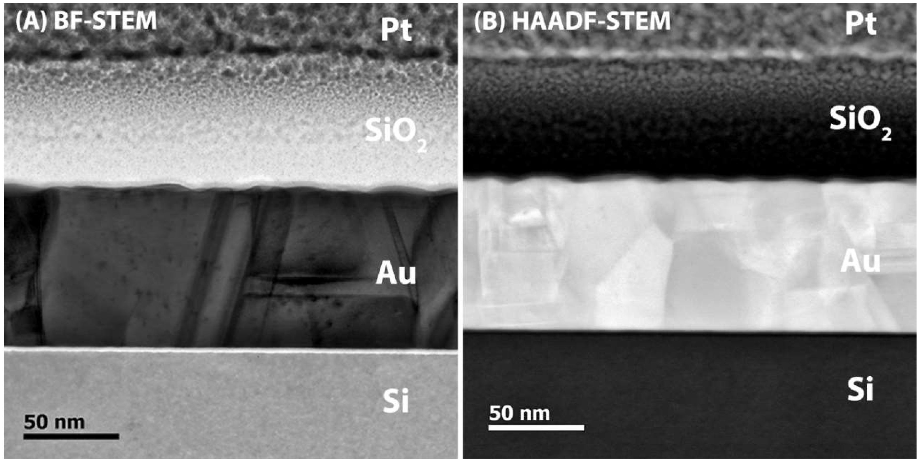
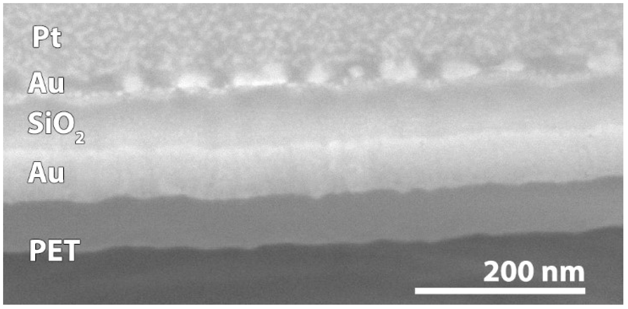
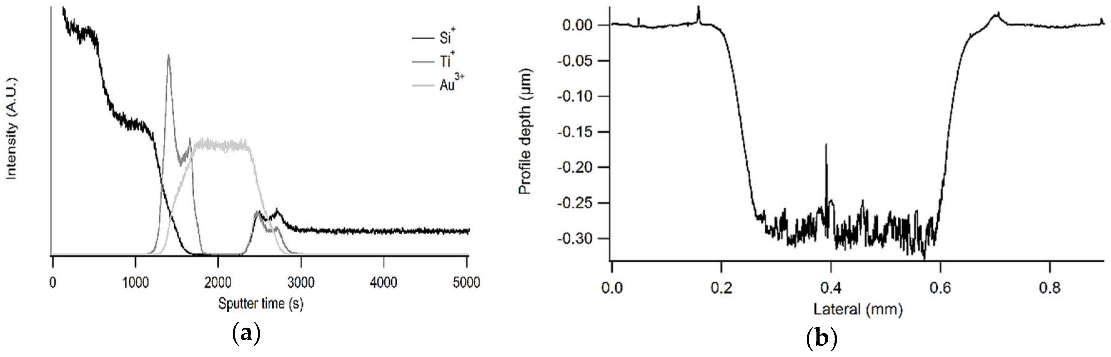
| Model Substrate | SIMS (nm) | EM (nm) | Ellipsometry (nm) |
|---|---|---|---|
| TiO2/Au/silicon (a) | – | 63.9 | 88.2 |
| TiO2/Au/silicon (b) | 63.6 ± 5.7 | 61.8 | 92.9 |
| TiO2/Au/PET (a) | 61.0 ± 6.3 | 57.5 | 95.2 |
| TiO2/Au/PET (b) | 84.7 ± 8.2 | 82.8 | 77.8 |
| Window film (a) | 126 ± 8 | X | X |
| Window film (b) | 274 ± 12 | X | X |
© 2018 by the authors. Licensee MDPI, Basel, Switzerland. This article is an open access article distributed under the terms and conditions of the Creative Commons Attribution (CC BY) license (http://creativecommons.org/licenses/by/4.0/).
Share and Cite
Van Zele, M.; Watté, J.; Hasselmeyer, J.; Rijckaert, H.; Vercammen, Y.; Verstuyft, S.; Deduytsche, D.; Debecker, D.P.; Poleunis, C.; Van Driessche, I.; et al. Thickness Characterization Toolbox for Transparent Protective Coatings on Polymer Substrates. Materials 2018, 11, 1101. https://doi.org/10.3390/ma11071101
Van Zele M, Watté J, Hasselmeyer J, Rijckaert H, Vercammen Y, Verstuyft S, Deduytsche D, Debecker DP, Poleunis C, Van Driessche I, et al. Thickness Characterization Toolbox for Transparent Protective Coatings on Polymer Substrates. Materials. 2018; 11(7):1101. https://doi.org/10.3390/ma11071101
Chicago/Turabian StyleVan Zele, Matthias, Jonathan Watté, Jan Hasselmeyer, Hannes Rijckaert, Yannick Vercammen, Steven Verstuyft, Davy Deduytsche, Damien P. Debecker, Claude Poleunis, Isabel Van Driessche, and et al. 2018. "Thickness Characterization Toolbox for Transparent Protective Coatings on Polymer Substrates" Materials 11, no. 7: 1101. https://doi.org/10.3390/ma11071101