Terahertz Spectroscopy of Amorphous WSe2 and MoSe2 Thin Films
by
 ,
,
Gianpaolo Papari
1,2,* ,
,
Can Koral
1,2,
Toby Hallam
3,4,
Georg Stefan Duesberg
3,5 and
Antonello Andreone
1,2 1
Dipartimento di Fisica, Università di Napoli “Federico II,” Piazzale Tecchio 80, I-80125 Naples, Italy
2
CNR-SPIN, UOS Napoli, via Cinthia, I-80126 Naples, Italy
3
CRANN & AMBER Center, School of Chemistry, Trinity College Dublin, Dublin 2, Ireland
4
School of Engineering, Newcastle University, Merz Court, Newcastle upon Tyne NE1 7RU, UK
5
Institute of Physics, EIT 2, Faculty of Electrical Engineering and Information Technology, Universität der Bundeswehr München, Werner-Heisenberg-Weg 39, EIT2, 85577 Neubiberg, Germany
*
Author to whom correspondence should be addressed.
Materials 2018, 11(9), 1613; https://doi.org/10.3390/ma11091613
Submission received: 10 August 2018
/
Revised: 28 August 2018
/
Accepted: 30 August 2018
/
Published: 4 September 2018
(This article belongs to the Special Issue Materials for Sources and Detectors in the GIGA-TERA-MIR Range)
Abstract
:Time domain spectroscopy is used to determine the THz electromagnetic response of amorphous transition metal dichalcogenides WSe2 and MoSe2 in thin-film form. The dielectric function is obtained using a rigorous transmission model to account for the large etalon effect. The Drude–Smith model is applied to retrieve the dielectric function, and from there, the sample conductivity.
1. Introduction
Transition metal dichalcogenides (TMDs) are characterized by a layered structure, responsible for their peculiar intrinsic 2-D electronic properties. Each crystal plane is based on the chemical configuration MX2, where M is a metal and X is a chalcogen [1,2]. Adjacent layers are held together by van der Waals forces, which inhibits free charge mobility across MX2 planes. TMDs in thin-film form offer a large variety of compounds with adjustable band gaps [3,4] and present a good transparency in the THz band that might pave the way to the development of a promising class of novel devices for THz optoelectronics [4]. Different from other tunable band gap systems like graphene, TMDs can also exploit an additional external parameter to control their own electro-optic properties as the magnetic field because of the spin-dependent band gap [5].
Furthermore, it has been shown [1,6,7] that the energy band structure of TMDs presents an interesting and unique dependence on the layer number, and a band gap transition from indirect to direct one for monolayer samples. Consequently, there is a consistent and growing demand in thin-film characterization, for the possible development of novel fast electronic [8,9] and/or electro-optical systems [10,11]. Recent advances in materials, sources, and detectors from the sub-THz and THz [3] to the mid-infrared [1,4,6] highlight the importance of time domain spectroscopy (TDS) to determine material properties at very high frequencies, such as the refractive index, absorption loss, and complex conductivity [12,13,14,15].
Nowadays, experimental strategies (see, for instance, Reference [16]), along with the application of proper theoretical models [17] and computational techniques [18,19,20,21], render the use of THz waves a robust and effective tool for thin-film characterization. Nevertheless, the presence in a majority of cases of a substrate unavoidably affects the fast (1–2 ps) time signal and produces a number of reflected copies, introducing sinusoidal (Fabry–Perot) oscillations in the Fourier transform of the transmitted and/or reflected wave. As long as the substrate is reasonably thick to induce a consistent time shift between the main signal and its copies, it is possible to cut them, applying a proper temporal windowing [22,23]. Of course, this procedure is recommended only when it does not affect the structure of the main signal. Otherwise, in the extraction of the electrodynamic parameters (EPs) of the sample under test, one runs the risk of losing relevant information.
Among several TMD composites, the Se based thin-films still lack investigation with linear THz spectroscopy. Here, we extract the electrodynamic parameters of amorphous WSe2 and MoSe2 films, 20 nm thick, deposited on a crystalline SiO2 substrate having a thickness of about 300 µm (d ≈ λ). Choosing a relatively thin substrate, the measurements suffer lower losses, but the transmitted signal shows a reflected copy too close to the main signal to be cut away. To minimize the unavoidable Fabry–Perot oscillations in EPs, we apply a reliable and simple method based on the transfer function (TF) equations [17]. In particular we retrieve the dielectric function (), and from there, we extract intrinsic parameters, such as the plasma frequency and the DC conductivity through the Drude–Smith model [24].
2. Thin-Film Fabrication and Characterization
2.1. TMD Deposition, and Morphological and Compositional Analysis
The TMD films have been deposited using a process known as thermally assisted conversion (TAC). TAC has the capability of depositing a continuous large-scale film with multiple layers [25]. The appropriate transition metal (Mo, W) films were deposited using a sputter coater (PECS, Gatan, Pleasanton, CA, USA) at <2 Å/s to form a smooth conformal coating 10 nm thick on a c-axis SiO2 substrate. In order to convert the metal films with their respective diselenides, they were exposed to selenium vapor at an elevated temperature in a home-built hot-wall chemical vapor deposition reactor with a process that has been described in more detail previously [3]. Specifically, metal films were converted to selenide in the reactor with chamber temperature at 600 °C under a flow of about 150 sccm of argon with the Se powder source held upstream at 219 °C for 2 h. Previous characterization indicated that the final thickness of selenide (MoSe2, WSe2) was 20 nm, which was double the initial metal thickness. To protect the films from oxidants in the atmosphere, they were encapsulated with 5 nm of Al2O3 using atomic layer deposition carried out over 46 cycles at 80 °C and a pressure of 2.2 Torr.
Using a shadow mask, samples were deposited on one half of SiO2 c-axis substrates having a total area of 2 cm × 1 cm. The second half was intentionally left bare, so that one could retrieve the thin-film parameters employing the exact film thickness and refractive index of the specific substrate on which each sample was deposited. As it will be shown in detail in the next paragraph, this was the only effective procedure to minimize the error introduced by the unavoidably slight difference in substrate parameters [16,23].
To evaluate the thickness profile and roughness, and check the morphology of the films under investigation, atomic force microscopy (AFM) measurements were carried out in a non-contact mode by using a Park Instruments XE-100 atomic force microscope in tapping mode.
To evaluate the chemical composition of the sample, X-ray photoelectron spectroscopy (XPS) was performed using a VG Scientific ESCAlab MKII system with a CLAM2 analyzer and PSP twin anode, unmonochromatized Al Kα X-ray source. Spectral fitting was performed using CasaXPS software. Charge compensation used the adventitious carbon peak at 284.6 eV. A Shirley background subtraction was performed, followed by the fitting of transition metal and chalcogen doublet peaks with mixed Gaussian and Lorentzian character.
2.2. Experimental Techniques
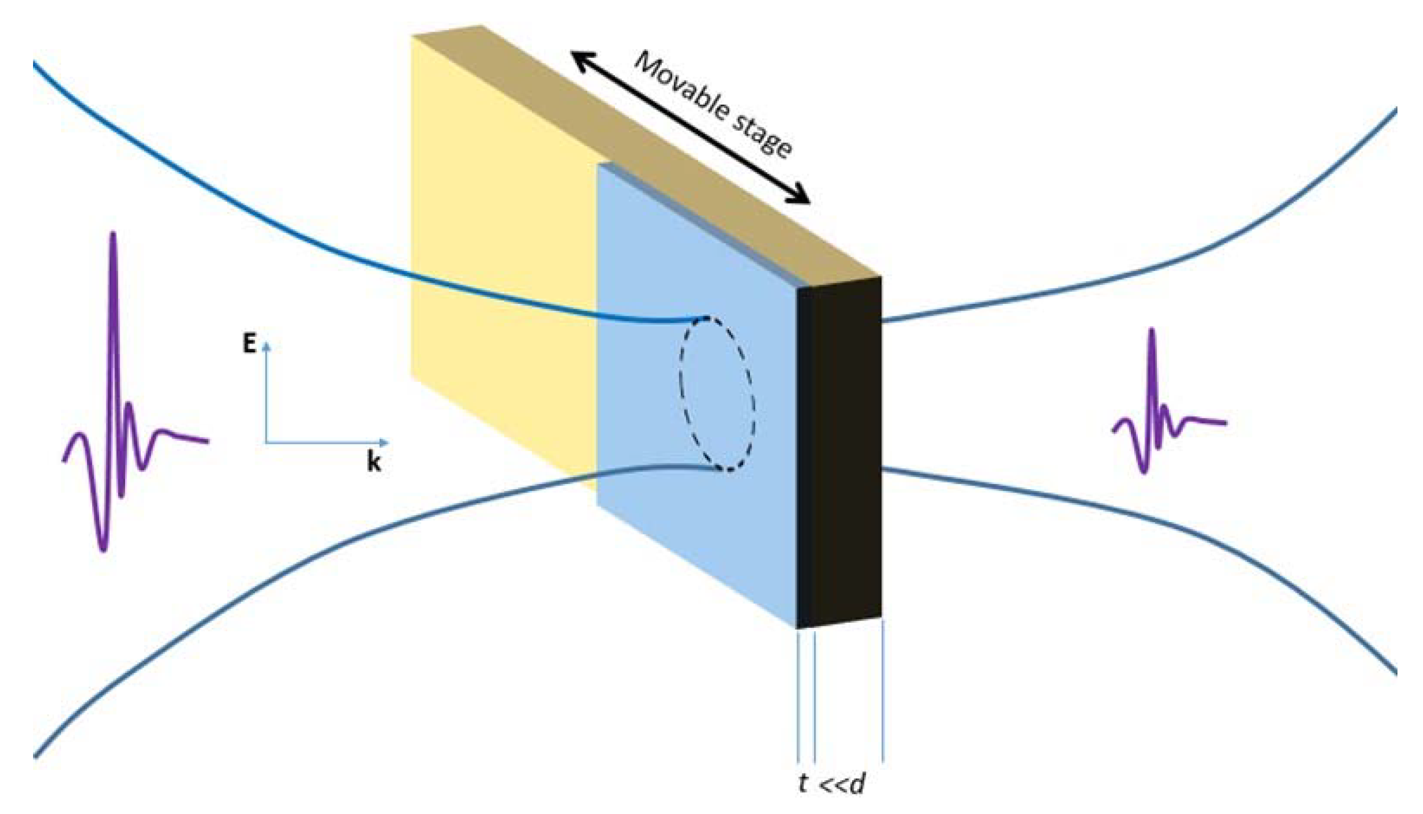
The measurement setup was similar to the one adopted in other experiments performed earlier [26,27]. Briefly, the sample was mounted over a hollow support of aluminum allowing us to measure, in a row, the signal transmitted through the free space, , the bare substrate, , and the film, ). A step motor controlled the position where the THz pulse impinged the support. The procedure is schematically shown in Figure 1. The size of the Gaussian profile of the focused THz pulse, estimated with the standard knife-edge technique, was of the order of 2 mm. In order to remove unwanted spectral features related to water absorption, measurements were performed in an N2 environment with a nominal humidity level below 1%. TDS was performed using a commercial THz system (Menlo SystemsTM, Martinsried, Germany) that generated and detected a pulsed THz signal, having a repetition rate of about 80 MHz. The physical process, for both generation and detection, was based on the down conversion of an optical pulse exciting a photoconductive antenna nested over a GaAs film. Temporal pulsed signals, of duration 1–2 ps, were acquired for about 200 ps, resulting in a frequency resolution of about 5 GHz and a useful bandwidth in the interval 0.15–3 THz.
3. Theoretical Background
Routine procedures for the retrieval of the complex electrodynamic parameters of a single or a multilayer sample have been settled for years and goes under the name of the transfer function (TF) model [28,29]. Specifically, when the electromagnetic signal passes through a film having thickness t deposited on a dielectric substrate, the transfer function in the frequency domain can be written as [17]:
where
represents the Fabry–Perot factor [29]. Subscripts a, s, and f in the complex refractive index refers to air, the substrate, and the TMD film respectively. Equation (1) suggests that and affect the modulus and phase of transmission in such a way that a specific numerical algorithm has to be applied [28]. Specifically, this algorithm, called the total variation technique (TVT) extracts the refractive index of the sample by minimizing the difference between the experimental and theoretical transmission curve [28]. We first extracted the refractive index of the substrate by employing the simple expression of the transfer function for a single layer [29]. The use of the TVT in the simple case of a thick substrate enabled us to get both and also the effective thickness deff of the substrate [18]. In our measurements, as well as deff values were extracted by using the commercial software TeralyzerTM (Martinsried, Germany). Since deff was determined with an accuracy of ±2 µm, this translates into a relative error lower than 1% for both the real and imaginary components of the substrate dielectric function. Once and deff were known, Equation (1) was then applied to get using the total variation technique routine, with a total relative error estimated to be about 10% for the samples under investigation. The error in the evaluation of was mostly related to the uncertainty in the film thickness due to the surface roughness that in our case was of the order of 4 nm. In the following graphs, this error was usually well within the scattered data point size.
In general, once is found, the real and imaginary parts of the dielectric function could be obtained using the standard formulas and .
Within the TF model, the effective thickness deff and refractive index of the bare substrate are given by the values determining the minimum FP oscillations [19]. However, “residual ripples” are always present in all calculated electrodynamic parameters, hence a systematic approach to smooth them without altering the effective physical quantities is a recommended strategy. Towards this aim, it is worth first to mention that it is better to deal with FP residual oscillations only at the very end of the retrieval process, once a “universal” dielectric function (expressible as the sum of the monotonic trend and the oscillating contribution) has been determined with an accurate measure of the substrate thickness. In this way, a reference frequency interval ∆f to apply an adjacent point average procedure with is univocally determined by the physical condition on the extinction coefficient of the substrate: (ω) ≥ 0. Then, the number of points used for the smoothing process is essentially set by the number of points contained in a single FP oscillation, which in our case was of the order of 50.
To describe the dependence of the complex dielectric/conductivity function on the intrinsic material parameters related to the mean dynamics of free charges, the standard and widely used approach is the Drude–Smith (DS) model [24]. In this framework the dielectric function is given by
where is the plasma frequency, = 1/τ is the relaxation frequency, is an asymptotic constant, and accounts for the backscattered particles and assumes values between −1 and 0. From the dielectric function the complex conductivity can be easily obtained using the relation
where is the vacuum permittivity. After the fitting procedure, one can yield the sample zero frequency conductivity as .
4. Results
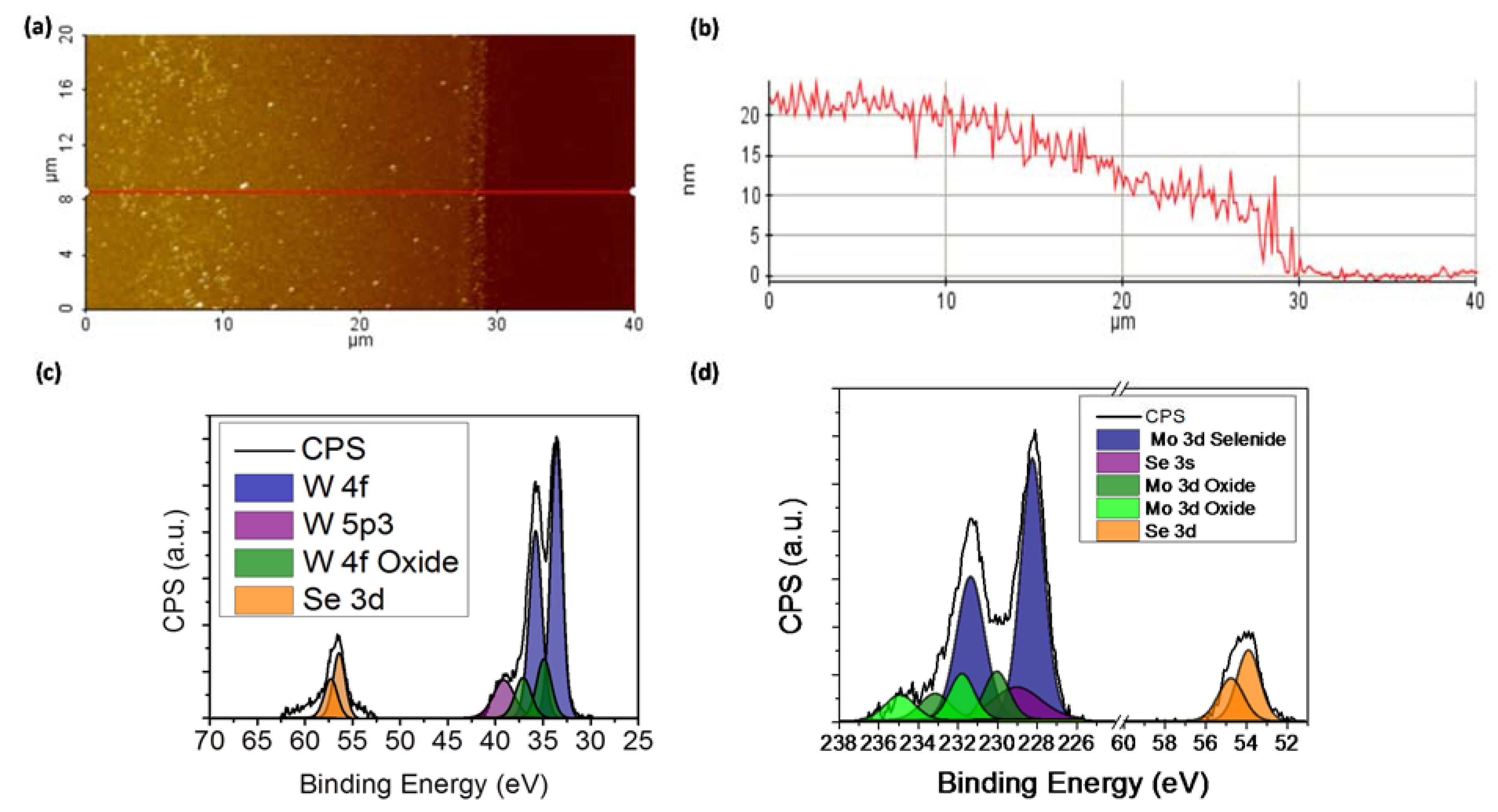
An AFM image of the MoSe2 sample is reported in Figure 2a. The image shows the step generated by the shadow mask between the substrate and the film enabling us to measure the surface profile along the red line as presented in Figure 2b. Because of the shadow mask, the MoSe2 thickness slowly decreased from about 20 nm to 0 with a roughness of 4 nm at most. The WSe2 sample was characterized by similar roughness, although the film edge was decorated by a series of flakes a few microns large
A core level XPS spectrum of WSe2 grown at 600 °C is shown in Figure 2c. A deconvolution process allowed for highlighting, through Gaussian-Lorentzian like curves, the binding energies of atoms composing the material. The majority of the metal was bound to selenium, which was manifest as the large doublet (blue) at 33 eV with some residual oxides present (green). The spin-orbit splitting in the W 4f doublets was 2.18 eV and the branching ratio (W 4f5/2 to W 4f7/2) was 3:4. A background contribution existed around the selenium peak (orange), which could have been due to excess amorphous Se on the surface. Using relative sensitivity factors (RSFs) and comparing the area under the peaks, the atomic ratio was found to be 1.7, with a possible underestimation due to the difficulty in deconvoluting the Se peak from the background.
As shown in Figure 2d, the Mo 3d core-level could be fitted with one main component at a binding energy of 228–229 eV for the Mo 3d5/2 peak (blue), which originated from selenised Mo, and one smaller component on the high binding energy side of the peak (green), which was most likely related to residual oxides [25]. The spin-orbit splitting in the Mo 3d doublets was 3.14 eV and the branching ratio (Mo 3d3/2 to Mo 3d5/2) was 2:3. All components of the Mo 3d line have been fitted using a mixed Gaussian-Lorentzian line shape with a FWHM of 1.3 ± 0.2 eV. These spectra were complicated to deconvolute by the fact that they lie on top of the Se 3s level, which has been fitted with a FWHM of 3.5 eV (purple) and normalized to the Se 3d. The Se 3d core-level (orange) could be fitted with only one component at a binding energy of 55 eV, indicating that there was no unreacted selenium on the surface. The stoichiometric atomic ratio was found to be close to 2. Thus, the oxide contributions were found to be minimal, below 5%, which was most likely a surface oxide, occurring while the samples were exposed to an ambient environment prior to XPS analysis.
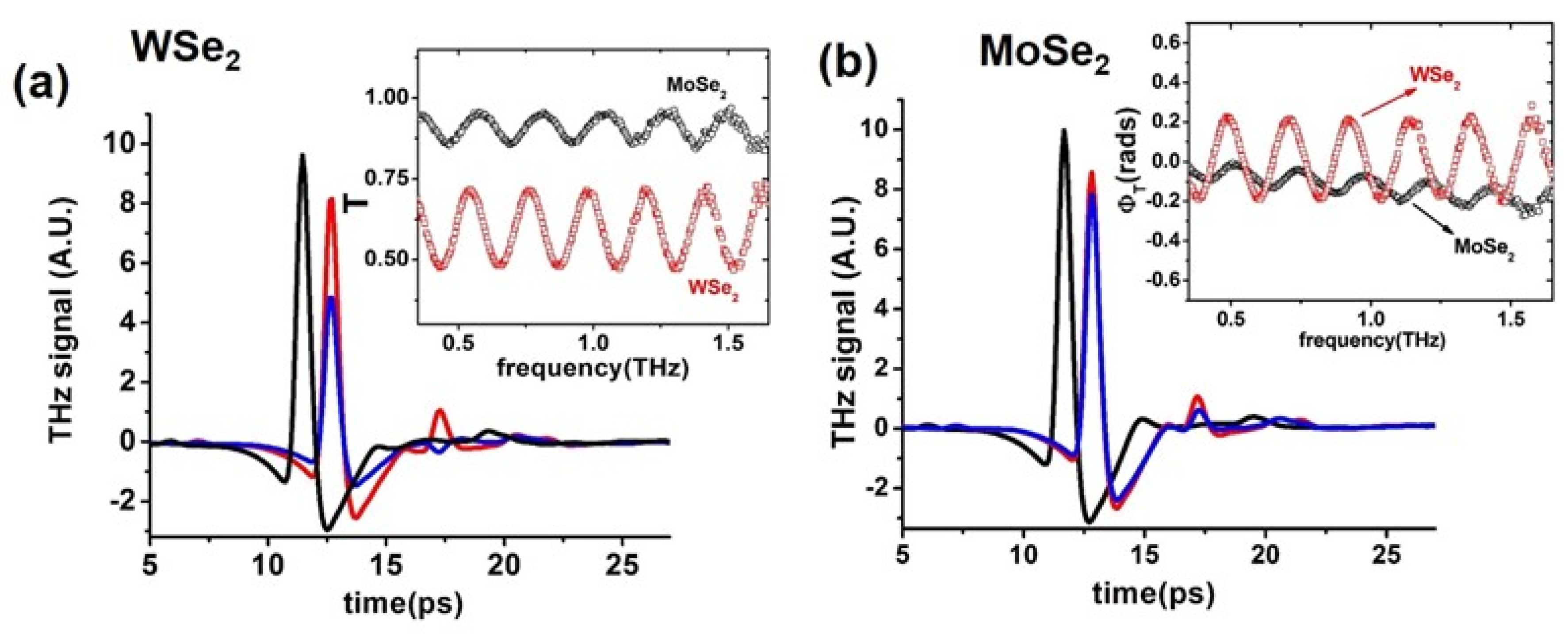
In Figure 3a,b, the temporal evolution of the electric field signals transmitted across the WSe2 and MoSe2 samples, given by blue curves, is reported. In the same graphs, black curves represent the free space transmission, whereas red curves refer to signals passing through the bare substrate. Peak amplitude in the substrate was always around 20% lower than the free space case, and its delay of about ≈ 2 ps described the proper change in refractive index (since the nominal thickness was 300 µm, this corresponds to ≈ 2 for the crystalline SiO2). The presence of the WSe2 and MoSe2 thin-film induced a further reduction in the transmitted signal (blue curves) of about 30% and 10%, respectively, when compared to the bare substrate. In all cases, THz waves impinging and passing through each sample caused an etalon effect with the first reflected signal manifesting itself with a delay of almost 5 ps from the main peak. Time dependent signals were then converted in the frequency domain using a fast Fourier transform (FFT) method, since EPs are directly related to the transmission function , where the complex quantities and are the FFT curves of the sample and bare substrate, respectively. In the inset of Figure 4a,b, the modulus and phase of the transmission functions for the two TMD samples are reported, respectively. Both quantities and show a robust FP oscillation whose period was of the order of , in agreement with the fact that the first echo had a delay with respect to the main signal of the order of [29]. Since we observed no substantial difference between the THz signals acquired on a bare substrate and one covered by 5 nm of Al2O3, in the data extraction, we neglected the presence of alumina on the TMD surface. On average, the transmission modulus of the MoSe2 film was about 0.9, whereas in the WSe2 sample, it strongly oscillated around 0.6. As for the phase, in the case of WSe2, it remained substantially constant around zero, as opposed to the MoSe2, where it showed a slight decrease, reflected in a larger dynamics of refractive index [n(ω) ≈ 1 − c (ω)/ωd] [29]. Applying the total variation technique, we found that the effective thickness of the substrates were deff (WSe2) = (332 ± 2) μm and deff (MoSe2) = (316 ± 2) μm. Using these values, we could then find . In the inset of Figure 4d, the refractive index and the extinction coefficient of the c-axis SiO2 substrate are reported. At f = 1 THz, = 2.05 ± 0.02 and = in substantial agreement with previous works [30,31].
5. Discussion
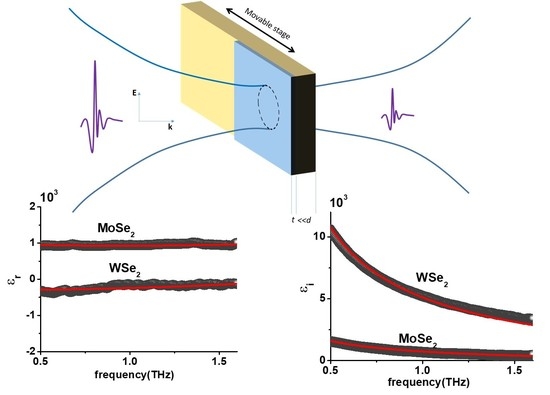
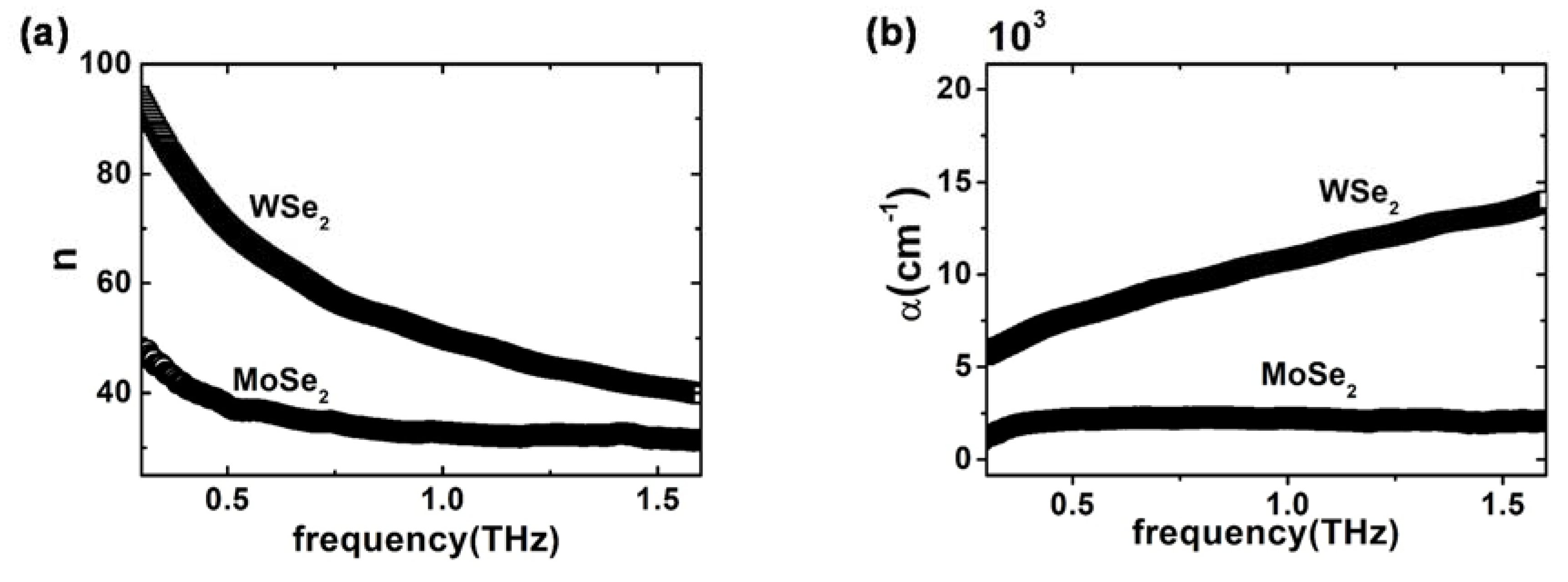
The substrate refractive index can be used by Equation (1) to calculate . In Figure 4a,b, the refractive index and the absorption coefficient of the two TMD films are shown, respectively. WSe2 showed a higher value of both the refractive index and extinction coefficient compared to MoSe2. In particular, absorption in WSe2 was higher than in MoSe2 by almost a factor of 5, with a well-defined positive slope, whereas saturated at about 2000 cm−1 in the range of 0.5–1.5 THz. and in the measured WSe2 and MoSe2 samples were consistent with those of a doped semiconducting material. Indeed, they were larger than GaAs [22], but lower than pure metallic thin-films [20].
Same results are presented in Figure 4c,d, here in terms of the real and imaginary part respectively of the complex dielectric function. The real part (Figure 4c) displays substantial flat dynamics, with MoSe2 characterized by a very high dielectric constant (≈1000) and WSe2 values being slightly negative. Imaginary parts of the two films are reported in Figure 4d, showing the expected free-charge decrease, although values for (WSe2) were larger than for (MoSe2) by a factor of 5 or more. The MoSe2 film, therefore, showed a semiconducting behavior [20,31] with the real part being strictly positive and a fast decay of versus frequency [32]. On the other hand, the WSe2 sample clearly presented a weak metallic behavior in the THz region, showing a complete negative and large values for .
Fitting curves on the retrieved dielectric functions of WSe2 and MoSe2 films, obtained via the DS model, are reported as continuous red lines in the same figures. The used fitting parameters are reported in Table 1, with an uncertainty of about 5%.
The higher conductivity of WSe2 with respect to MoSe2 mainly resulted in larger values of and smaller values of , as expected.
Nevertheless, the frequency response of the dielectric function and the values retrieved for the DC conductivity using the DS model was in clear contrast to what is observed in single crystal samples [33]. The observed metallic behavior may be ascribed to the presence of conductive channels in grain boundaries. A high density of metallic grain boundaries can in fact spontaneously form in slightly Se-deficient Mo thin films grown by molecular-beam epitaxy molecular-beam epitaxy [34]. We speculate that the same mechanism may apply to WSe2 samples. This would also explain the larger values of conductivity in the latter case.
6. Conclusions
We have retrieved the dielectric function of conducting MoSe2 and WSe2 TMDs by using time domain terahertz spectroscopy. Thin films have been created via a thermally assisted conversion process, which produced samples with good homogeneity. XPS measurements revealed the presence of a residual portion of uncombined metal particles, and therefore a TM:Se ratio smaller than 1:2. Ab initio thermodynamic simulations have shown [35] that this may favor the formation of dichalcogen-deficient grain boundaries instead of Se vacancies during the growth process. We have extracted the electrodynamic parameters of thin films deposited on 300 µm thick substrates, which introduce a relatively strong FP effect in transmission data. By applying a rigorous protocol based on the TF model and a self-consistent moving average procedure, we have minimized the periodic FP oscillations and fitted with the Drude–Smith function. The relatively high conductivity observed in both compounds may be ascribed to a high density of line defects presenting a metallic character.
The relatively high transparence along with the conducting features are encouraging in view of a possible use of TMD-based thin-films for applications as tunable metadevices in the THz region. The observed conducting nature can represent a promising alternative for the realization of new devices with higher currents and lower contact resistance.
Author Contributions
Conceptualization G.P., Software C.K. and G.P., Data Curation G.P., C.K., T.H. and G.S.D., Methodology T.H. and G.S.D., Validation G.S.D. and A.A., Writing-Original Draft Preparation, G.P., Writing-Review & Editing G.P. and A.A., supervision A.A.
Funding
G.S.D. acknowledges support from the Science Foundation Ireland (SFI) under 12/RC/2278 and 15/IA/3131 and the European Union Seventh Framework Program under Graphene Flagship Contract No 785219.
Acknowledgments
We acknowledge Fabio Chiarella for the AFM images. We further acknowledge Riley Gatensby, Katia O´Neill and Rita Sirs for sample characterization.
Conflicts of Interest
The authors declare no conflict of interest.
References
- Wang, Q.H.; Kalantar-Zadeh, K.; Kis, A.; Coleman, J.N.; Strano, M.S. Electronics and optoelectronics of two-dimensional transition metal dichalcogenides. Nat. Nanotechnol. 2012, 7, 699–712. [Google Scholar] [CrossRef] [PubMed] [Green Version]
- Jariwala, D.; Sangwan, V.K.; Lauhon, L.J.; Marks, T.J.; Hersam, M.C. Emerging Device Applications for Semiconducting Two-Dimensional Transition Metal Dichalcogenides. ACS Nano 2014, 8, 1102–1120. [Google Scholar] [CrossRef] [PubMed] [Green Version]
- Gatensby, R.; Hallam, T.; Lee, K.; McEvoy, N.; Duesberg, G.S. Investigations of vapour-phase deposited transition metal dichalcogenide films for future electronic applications. Solid State Electron. 2016, 125, 39–51. [Google Scholar] [CrossRef]
- Chen, Y.; Xi, J.; Dumcenco, D.O.; Liu, Z.; Wang, D.; Shuai, Z.; Huang, Y.; Xie, L. Tunable Band Gap in Atomically Thin Transition-Metal Dichalcogenide Alloys. ACS Nano 2013, 7, 4610–4616. [Google Scholar] [CrossRef] [PubMed]
- Xu, X. Spin and pseudospins in transition metal dichalcogenides. Nat. Phys. 2014, 10, 343–351. [Google Scholar] [CrossRef]
- Guo, H.Y.; Lu, N.; Wang, L.; Wu, X.J.; Zeng, X.C. Tuning Electronic and Magnetic Properties of Early Transition-Metal Dichalcogenides via Tensile Strain. J. Phys. Chem. C 2014, 118, 7242–7249. [Google Scholar] [CrossRef] [Green Version]
- Li, Y.; Tongay, S.; Yue, Q.; Kang, J.; Wu, J.; Li, J. Metal to semiconductor transition in metallic transition metal dichalcogenides. J. Appl. Phys. 2013, 114. [Google Scholar] [CrossRef]
- Docherty, C.J.; Parkinson, P.; Joyce, H.J.; Chiu, M.-H.; Chen, C.-H.; Lee, M.-Y.; Li, L.-J.; Herz, L.M.; Johnston, M.B. Ultrafast transient terahertz conductivity of monolayer MoS2 and WSe2 grown by chemical vapor deposition. ACS Nano 2014, 8, 11147–11153. [Google Scholar] [CrossRef] [PubMed]
- Lui, C.H.; Frenzel, A.J.; Pilon, D.V.; Lee, Y.H.; Ling, X.; Akselrod, G.M.; Kong, J.; Gedik, N. Trion-induced negative photoconductivity in monolayer MoS2. Phys. Rev. Lett. 2014, 113, 166801. [Google Scholar] [CrossRef] [PubMed]
- Tian, H.; Chin, M.L.; Najmaei, S.; Guo, Q.; Xia, F.; Wang, H.; Dubey, M. Optoelectronic devices based on two-dimensional transition metal dichalcogenides. Nano Res. 2016, 1, 1543–1560. [Google Scholar] [CrossRef]
- Sun, Z.; Martinez, A.; Wang, F. Optical modulators with 2D layered materials. Nat. Photonics 2016, 10, 227–238. [Google Scholar] [CrossRef] [Green Version]
- Pereira, M.F.; Zubelli, J.P.; Winge, D.; Wacker, A.; Rodrigues, A.S.; Anfertev, V.; Vaks, V. Theory and measurements of harmonic generation in semiconductor superlattices with applications in the 100 GHz to 1 THz range. Phys. Rev. B 2017, 96, 045306. [Google Scholar] [CrossRef] [Green Version]
- Pereira, M.F. The linewidth enhancement factor of intersubband lasers: From a two-level limit to gain without inversion conditions. Appl. Phys. Lett. 2016, 109, 222102. [Google Scholar] [CrossRef] [Green Version]
- Oriaku, C.I.; Pereira, M.F. Analytical solutions for semiconductor luminescence including Coulomb correlations with applications to dilute bismides. J. Opt. Soc. Am. B 2017, 34, 321–328. [Google Scholar] [CrossRef]
- Pereira, M. Analytical Expressions for Numerical Characterization of Semiconductors per Comparison with Luminescence. Materials (Basel) 2017, 11, 2. [Google Scholar] [CrossRef] [PubMed]
- Walther, M.; Cooke, D.G.; Sherstan, C.; Hajar, M.; Freeman, M.R.; Hegmann, F.A. Terahertz conductivity of thin gold films at the metal-insulator percolation transition. Phys. Rev. B Condens. Matter Mater. Phys. 2007, 76, 125408. [Google Scholar] [CrossRef]
- Duvillaret, L.; Garet, F.; Coutaz, J.-L.L. A reliable method for extraction of material parameters in terahertz time-domain spectroscopy. IEEE J. Sel. Top. Quantum Electron. 1996, 2, 739–746. [Google Scholar] [CrossRef]
- TDorney, D.; Baraniuk, R.G.; Mittleman, D.M. Material parameter estimation with terahertz time-domain spectroscopy. J. Opt. Soc. Am. A Opt. Image Sci. Vis. 2001, 18, 1562–1571. [Google Scholar] [CrossRef]
- Pupeza, I.; Wilk, R.; Koch, M. Highly accurate optical material parameter determination with THz time-domain spectroscopy. Opt. Express 2007, 15, 4335–4350. [Google Scholar] [CrossRef] [PubMed]
- Zhou, D.; Parrott, E.; Paul, D. Determination of complex refractive index of thin metal films from terahertz time-domain spectroscopy. J. Appl. Phys. 2008, 104, 53110. [Google Scholar] [CrossRef]
- Zaytsev, K.I.; Gavdush, A.A.; Karasik, V.E.; Alekhnovich, V.I.; Nosov, P.A.; Lazarev, V.A.; Reshetov, I.V.; Yurchenko, S.O. Accuracy of sample material parameters reconstruction using terahertz pulsed spectroscopy. J. Appl. Phys. 2014, 115, 193105. [Google Scholar] [CrossRef]
- Yasuda, H.; Hosako, I. Measurement of terahertz refractive index of metal with terahertz time-domain spectroscopy. Jpn. J. Appl. Phys. 2008, 47, 1632–1634. [Google Scholar] [CrossRef]
- Thoman, A.; Kern, A.; Helm, H.; Walther, M. Nanostructured gold films as broadband terahertz antireflection coatings. Phys. Rev. B Condens. Matter Mater. Phys. 2008, 77, 195405. [Google Scholar] [CrossRef]
- Smith, N. Classical generalization of the Drude formula for the optical conductivity. Phys. Rev. B 2001, 64, 155106. [Google Scholar] [CrossRef]
- Gatensby, R.; McEvoy, N.; Lee, K.; Hallam, T.; Berner, N.C.; Rezvani, E.; Winters, S.; O’Brien, M.; Duesberg, G.S. Controlled synthesis of transition metal dichalcogenide thin films for electronic applications. Appl. Surf. Sci. 2014, 297, 139–146. [Google Scholar] [CrossRef] [Green Version]
- Papari, G.P.; Gargiulo, V.; Alfè, M.; di Capua, R.; Pezzella, A.; Andreone, A. THz spectroscopy on graphene-like materials for bio-compatible devices. J. Appl. Phys. 2017, 121, 145107. [Google Scholar] [CrossRef]
- Papari, G.P.; Silvestri, B.; Vitiello, G.; de Stefano, L.; Rea, I.; Luciani, G.; Aronne, A.; Andreone, A. Morphological, Structural, and Charge Transfer Properties of F-Doped ZnO: A Spectroscopic Investigation. J. Phys. Chem. C 2017, 121, 16012–16020. [Google Scholar] [CrossRef]
- Angrisani, L.; Cavallo, G.; Liccardo, A.; Papari, G.; Andreone, A. THz Measurement systems. In New Trends and Developments in Metrology; Luigi, C., Ed.; InTech: England, UK, 2016. [Google Scholar]
- Withayachumnankul, W.; Naftaly, M. Fundamentals of measurement in terahertz time-domain spectroscopy. J. Infrared Millim. Terahertz Waves 2014, 35, 610–637. [Google Scholar] [CrossRef]
- Cataldo, G.; Beall, J.A.; Cho, H.-M.; McAndrew, B.; Niemack, M.D.; Wollack, E.J. Infrared dielectric properties of low-stress silicon oxide. Opt. Lett. 2012, 37, 4200–4202. [Google Scholar] [CrossRef] [PubMed]
- Lee, K.-S.; Lu, T.-M.; Zhang, X.-C. Tera Tool [terahertz time-domain spectroscopy]. IEEE Circuits Devices Mag. 2002, 18, 23–28. [Google Scholar]
- Titova, L.V.; Cocker, T.L.; Cooke, D.G.; Wang, X.; Meldrum, A.; Hegmann, F.A. Ultrafast percolative transport dynamics in silicon nanocrystal films. Phys. Rev. B Condens. Matter Mater. Phys. 2011, 83, 085403. [Google Scholar] [CrossRef]
- Kam, K.-K. Electrical Properties of WSe2, WS2, MoSe2, MoS2, and Their Use as Photoanodes in a Semiconductor Liquid Junction Solar Cell. Ph.D. Thesis, Iowa State University, Ames, IA, USA, 1982. [Google Scholar]
- Ma, Y.; Kolekar, S.; Diaz, H.C.; Aprojanz, J.; Miccoli, I.; Tegenkamp, C.; Batzill, M. Metallic Twin Grain Boundaries Embedded in MoSe 2 Monolayers Grown by Molecular Beam Epitaxy. ACS Nano 2017, 11, 5130–5139. [Google Scholar] [CrossRef] [PubMed]
- Lehtinen, O.; Komsa, H.; Pulkin, A.; Whitwick, M.B.; Chen, M.; Lehnert, T.; Mohn, M.J.; Yazyev, O.V.; Kis, A.; Kaiser, U.; et al. Atomic Scale Microstructure and Properties of Se-De fi cient. ACS Nano 2015, 9, 3274–3283. [Google Scholar] [CrossRef] [PubMed]
Figure 1.
Sketch of the experimental setup. The blue area represents the film deposited on half the SiO2 substrate (depicted in yellow). A step motor controlled the position of the sample with respect to the impinging THz pulse.
Figure 1.
Sketch of the experimental setup. The blue area represents the film deposited on half the SiO2 substrate (depicted in yellow). A step motor controlled the position of the sample with respect to the impinging THz pulse.

Figure 2.
Characterization of TMD films. (a) AFM image of MoSe2. The area between 30 and 40 µm represents the bare SiO2 substrate. (b) Surface profile of MoSe2 according to the red line presented in panel (a). (c,d) XPS data and spectral fitting of WSe2 and MoSe2, respectively.
Figure 2.
Characterization of TMD films. (a) AFM image of MoSe2. The area between 30 and 40 µm represents the bare SiO2 substrate. (b) Surface profile of MoSe2 according to the red line presented in panel (a). (c,d) XPS data and spectral fitting of WSe2 and MoSe2, respectively.

Figure 3.
(a) Black, red, and blue solid lines represent the time dependent THz signals referred for free space, SiO2 substrate, and WSe2 film + substrate, respectively. (b) Similar to (a), with the blue curve showing the measurement on the MoSe2 film + substrate. Left and right insets: Comparison between the magnitude and phase respectively of the transmission function for the two TMD samples.

Figure 4.
(a,b) show the refractive index n and the absorption coefficient respectively of the two samples. (c,d) report the real () and imaginary ( ) parts of dielectric function of TMD’s films as extracted by using the TF model. The red line corresponds to the Drude–Smith model fit whose parameters are reported in Table 1. Inset: refractive index and extinction coefficient versus frequency of the SiO2 substrate.


Table 1.
Best fit parameters for the dielectric functions of WSe2 and MoSe2 films using the DS model. Parameter accuracy is of the order of 5%.
Table 1.
Best fit parameters for the dielectric functions of WSe2 and MoSe2 films using the DS model. Parameter accuracy is of the order of 5%.
| Sample | |||||
|---|---|---|---|---|---|
| WSe2 | 850 | 16 | −0.22 | 3000 | 1200 |
| MoSe2 | 270 | 9.5 | −0.35 | 444 | 1220 |
© 2018 by the authors. Licensee MDPI, Basel, Switzerland. This article is an open access article distributed under the terms and conditions of the Creative Commons Attribution (CC BY) license (http://creativecommons.org/licenses/by/4.0/).
Share and Cite
MDPI and ACS Style
Papari, G.; Koral, C.; Hallam, T.; Duesberg, G.S.; Andreone, A. Terahertz Spectroscopy of Amorphous WSe2 and MoSe2 Thin Films. Materials 2018, 11, 1613. https://doi.org/10.3390/ma11091613
AMA Style
Papari G, Koral C, Hallam T, Duesberg GS, Andreone A. Terahertz Spectroscopy of Amorphous WSe2 and MoSe2 Thin Films. Materials. 2018; 11(9):1613. https://doi.org/10.3390/ma11091613
Chicago/Turabian StylePapari, Gianpaolo, Can Koral, Toby Hallam, Georg Stefan Duesberg, and Antonello Andreone. 2018. "Terahertz Spectroscopy of Amorphous WSe2 and MoSe2 Thin Films" Materials 11, no. 9: 1613. https://doi.org/10.3390/ma11091613
Note that from the first issue of 2016, this journal uses article numbers instead of page numbers. See further details here.