Effects of Interfacial Passivation on the Electrical Performance, Stability, and Contact Properties of Solution Process Based ZnO Thin Film Transistors


Abstract
:1. Introduction
2. Materials and Methods
2.1. Materials
2.2. Thin Films Preparation
2.3. Film Formation and Device Fabrication
2.4. Device Characterization
3. Results
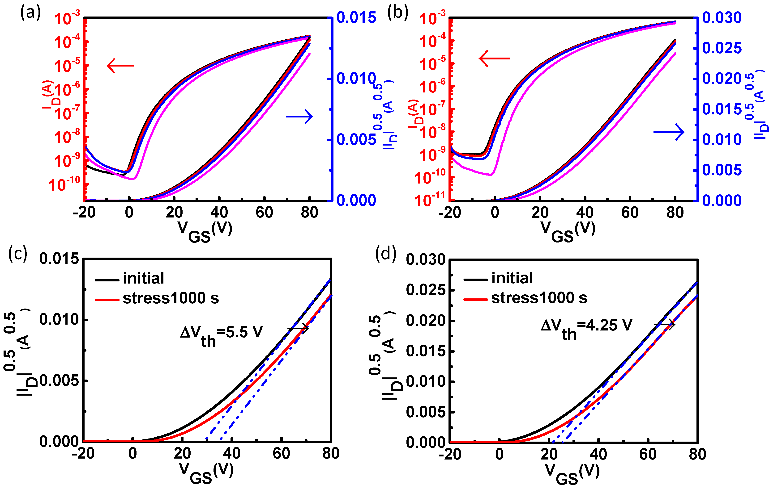
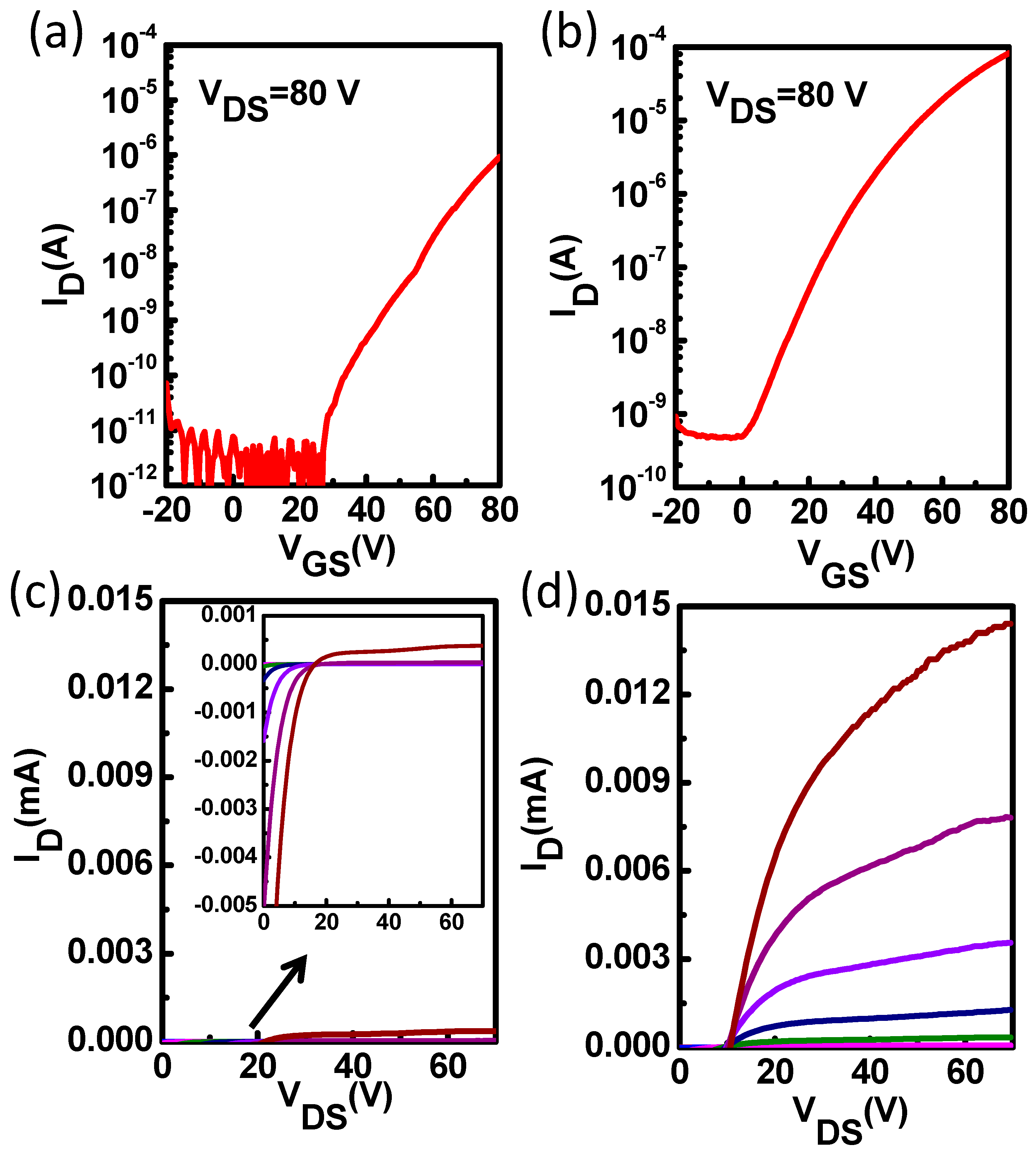
4. Conclusions
Supplementary Materials
Author Contributions
Funding
Conflicts of Interest
References
- Nayak, P.K.; Hedhili, M.N.; Cha, D.; Alshareef, H.N. High performance In2O3 thin film transistors using chemically derived aluminum oxide dielectric. Appl. Phys. Lett. 2013, 103, 1–5. [Google Scholar] [CrossRef]
- Banger, K.K.; Peterson, R.L.; Mori, K.; Yamashita, Y.; Leedham, T.; Sirringhaus, H. High performance, low temperature solution-processed barium and strontium doped oxide thin film transistors. Chem. Mater. 2014, 26, 1195–1203. [Google Scholar] [CrossRef] [PubMed]
- Kim, M.G.; Kanatzidis, M.G.; Facchetti, A.; Marks, T.J. Low-temperature fabrication of high-performance metal oxide thin-film electronics via combustion processing. Nat. Mater. 2011, 10, 382–388. [Google Scholar] [CrossRef] [PubMed]
- Kim, Y.H.; Heo, J.S.; Kim, T.H.; Park, S.; Yoon, M.H.; Kim, J.; Oh, M.S.; Yi, G.R.; Noh, Y.Y.; Park, S.K. Flexible metal-oxide devices made by room-temperature photochemical activation of sol-gel films. Nature 2012, 489, 128–132. [Google Scholar] [CrossRef] [PubMed]
- Hu, R.; Pei, Y.; Chen, Z.; Yang, J.; Li, Y.; Lin, J.; Zhao, Y.; Wang, C.; Liang, J.; Fan, B.; et al. Ultra-High Field-Effect Mobility Thin-Film Transistors with Metal Organic Chemical Vapor Deposition Grown In2O3 Channel Treated by Oxygen Microwave Plasma. IEEE Electron Device Lett. 2015, 36, 1163–1165. [Google Scholar] [CrossRef]
- Kang, C.; Kim, H.; Oh, Y.-W.; Baek, K.-H.; Do, L.-M. High-Performance, Solution-Processed Indium-Oxide TFTs Using Rapid Flash Lamp Annealing. IEEE Electron Device Lett. 2016, 37, 595–598. [Google Scholar] [CrossRef]
- Singh, T.B.; Jasieniak, J.J.; de Oliveira Tozi, L.; Easton, C.D.; Bown, M. Electrically Stable, Solution-Processed Amorphous Oxide IZO Thin-Film Transistors Through a UV-Ozone Assisted Sol-Gel Approach. IEEE Trans. Electron Devices 2014, 61, 1093–1100. [Google Scholar] [CrossRef]
- Kim, T.; Jang, B.; Bae, J.H.; Park, H.; Cho, C.S.; Kwon, H.J.; Jang, J. Improvement in the Performance of Sol-Gel Processed In2O3Thin-Film Transistor Depending on Sb Dopant Concentration. IEEE Electron Device Lett. 2017, 38, 1027–1030. [Google Scholar] [CrossRef]
- Chang, J.; Lin, Z.; Lin, M.; Zhu, C.; Zhang, J.; Wu, J. Solution processed F doped ZnO (ZnO:F) for thin film transistors and improved stability through co-doping with alkali metals. J. Mater. Chem. C 2015, 3, 1787–1793. [Google Scholar] [CrossRef]
- Esro, M.; Vourlias, G.; Somerton, C.; Milne, W.I.; Adamopoulos, G. High-mobility ZnO thin film transistors based on solution-processed hafnium oxide gate dielectrics. Adv. Funct. Mater. 2015, 25, 134–141. [Google Scholar] [CrossRef]
- Lin, Y.Y.; Hsu, C.C.; Tseng, M.H.; Shyue, J.J.; Tsai, F.Y. Stable and High-Performance Flexible ZnO Thin-Film Transistors by Atomic Layer Deposition. ACS Appl. Mater. Interfaces 2015, 7, 22610–22617. [Google Scholar] [CrossRef] [PubMed]
- Carcia, P.F.; McLean, R.S.; Reilly, M.H.; Nunes, G. Transparent ZnO thin-film transistor fabricated by rf magnetron sputtering. Appl. Phys. Lett. 2003, 82, 1117–1119. [Google Scholar] [CrossRef]
- Nishii, J.; Hossain, F.M.; Takagi, S.; Aita, T.; Saikusa, K.; Ohmaki, Y.; Ohkubo, I.; Kishimoto, S.; Ohtomo, A.; Fukumura, T.; et al. High mobility thin film transistors with transparent ZnO channels. Jpn. J. Appl. Phys. Part 2 Lett. 2003, 42, 0–3. [Google Scholar] [CrossRef]
- Jo, J.; Seo, O.; Choi, H.; Lee, B. Enhancement-mode ZnO thin-film transistor grown by metalorganic chemical vapor deposition. Appl. Phys. Express 2008, 1, 0412021–0412023. [Google Scholar] [CrossRef]
- Afouxenidis, D.; Mazzocco, R.; Vourlias, G.; Livesley, P.J.; Krier, A.; Milne, W.I.; Kolosov, O.; Adamopoulos, G. ZnO-based thin film transistors employing aluminum titanate gate dielectrics deposited by spray pyrolysis at ambient air. ACS Appl. Mater. Interfaces 2015, 7, 7334–7341. [Google Scholar] [CrossRef] [PubMed]
- Park, S.Y.; Kim, B.J.; Kim, K.; Kang, M.S.; Lim, K.H.; Lee, T.; Myoung, J.M.; Baik, H.K.; Cho, J.H.; Kim, Y.S. Low-temperature, solution-processed and alkali metal doped ZnO for high-performance thin-film transistors. Adv. Mater. 2012, 24, 834–838. [Google Scholar] [CrossRef] [PubMed]
- Song, K.; Noh, J.; Jun, T.; Jung, Y.; Kang, H.Y.; Moon, J. Fully flexible solution-deposited ZnO thin-film transistors. Adv. Mater. 2010, 22, 4308–4312. [Google Scholar] [CrossRef] [PubMed]
- Meyers, S.T.; Anderson, J.T.; Hung, C.M.; Thompson, J.; Wager, J.F.; Keszler, D.A. Aqueous inorganic inks for low-temperature fabrication of ZnO TFTs. J. Am. Chem. Soc. 2008, 130, 17603–17609. [Google Scholar] [CrossRef] [PubMed]
- Chang, J.; Lin, Z.; Zhu, C.; Chi, C.; Zhang, J.; Wu, J. Solution-Processed LiF-Doped ZnO Films for High Performance Low Temperature Field Effect Transistors and Inverted Solar Cells. ACS Appl. Mater. Interfaces 2013, 5, 6687–6693. [Google Scholar] [CrossRef] [PubMed]
- Chang, J.; Chang, K.L.; Chi, C.; Zhang, J.; Wu, J. Water induced zinc oxide thin film formation and its transistor performance. J. Mater. Chem. C 2014, 2, 5397–5403. [Google Scholar] [CrossRef]
- Lin, Z.; Chang, J.; Jiang, C.; Zhang, J.; Wu, J.; Zhu, C. Enhanced inverted organic solar cell performance by post-treatments of solution-processed ZnO buffer layers. RSC Adv. 2014, 4, 6646. [Google Scholar] [CrossRef]
- Lin, Z.; Chang, J.; Zhang, C.; Zhang, J.; Wu, J.; Hao, Y. Low temperature aqueous solution-processed Li doped ZnO buffer layers for high performance inverted organic solar cells. J. Mater. Chem. C 2016, 4, 6169–6175. [Google Scholar] [CrossRef]
- Lin, Z.; Chang, J.; Zhang, C.; Chen, D.; Wu, J.; Hao, Y. Enhanced Performance and Stability of Polymer Solar Cells by In Situ Formed AlOx Passivation and Doping. J. Phys. Chem. C 2017, 121, 10275–10281. [Google Scholar] [CrossRef]
- Park, J.-S.; Jeong, J.K.; Chung, H.-J.; Mo, Y.-G.; Kim, H.D. Electronic transport properties of amorphous indium-gallium-zinc oxide semiconductor upon exposure to water. Appl. Phys. Lett. 2008, 92, 72104. [Google Scholar] [CrossRef]
- Sung, S.-Y.; Choi, J.H.; Han, U.B.; Lee, K.C.; Lee, J.-H.; Kim, J.-J.; Lim, W.; Pearton, S.J.; Norton, D.P.; Heo, Y.-W. Effects of ambient atmosphere on the transfer characteristics and gate-bias stress stability of amorphous indium-gallium-zinc oxide thin-film transistors. Appl. Phys. Lett. 2010, 96, 102107. [Google Scholar] [CrossRef]
- Xiao, P.; Lan, L.; Dong, T.; Lin, Z.; Shi, W.; Yao, R.; Zhu, X.; Peng, J. InGaZnO thin-film transistors with back channel modification by organic self-assembled monolayers. Appl. Phys. Lett. 2014, 104. [Google Scholar] [CrossRef]
- Donley, C.; Dunphy, D.; Paine, D.; Carter, C.; Nebesny, K.; Lee, P.; Alloway, D.; Armstrong, N.R. Characterization of indium-tin oxide interfaces using X-ray photoelectron spectroscopy and redox processes of a chemisorbed probe molecule: Effect of surface pretreatment conditions. Langmuir 2002, 18, 450–457. [Google Scholar] [CrossRef]
- Hennek, J.W.; Smith, J.; Yan, A.; Kim, M.; Zhao, W.; Dravid, V.P.; Facchetti, A.; Marks, T.J. Oxygen “ Getter ” Effects on Microstructure and Carrier Transport in Low Temperature Combustion-Processed a—InXZnO (X = Ga, Sc, Y, La) Transistors. J. Am. Chem. Soc. 2013, 135, 10729–10741. [Google Scholar] [CrossRef] [PubMed]
- Kim, M.G.; Hennek, J.W.; Kim, H.S.; Kanatzidis, M.G.; Facchetti, A.; Marks, T.J. Delayed ignition of autocatalytic combustion precursors: Low-temperature nanomaterial binder approach to electronically functional oxide films. J. Am. Chem. Soc. 2012, 134, 11583–11593. [Google Scholar] [CrossRef] [PubMed]
- Feng, X.; Jiang, L. Design and creation of superwetting/antiwetting surfaces. Adv. Mater. 2006, 18, 3063–3078. [Google Scholar] [CrossRef]
- Gillan, L.; Leppäniemi, J.; Eiroma, K.; Majumdar, H.; Alastalo, A. High performance solution processed oxide thin-film transistors with inkjet printed Ag source-drain electrodes. J. Mater. Chem. C 2018, 6, 3220–3225. [Google Scholar] [CrossRef]
- Du, X.; Flynn, B.T.; Motley, J.R.; Stickle, W.F.; Bluhm, H.; Herman, G.S. Role of Self-Assembled Monolayers on Improved Electrical Stability of Amorphous In-Ga-Zn-O Thin-Film Transistors. ECS J. Solid State Sci. Technol. 2014, 3, Q3045–Q3049. [Google Scholar] [CrossRef] [Green Version]
- Length, A.C. InGaZnO Thin-Film Transistors Modified by Self-Assembled Monolayer With Different. IEEE Electron Device Lett. 2015, 36, 687–689. [Google Scholar] [CrossRef]
- Tao, Y.T. Structural Comparison of Self-Assembled Monolayers of n-Alkanoic Acids on the Surfaces of Silver, Copper, and Aluminum. J. Am. Chem. Soc. 1993, 115, 4350–4358. [Google Scholar] [CrossRef]
- Ueoka, Y.; Ishikawa, Y.; Bermundo, J.P.; Yamazaki, H.; Urakawa, S.; Osada, Y.; Horita, M.; Uraoka, Y. Effect of contact material on amorphous InGaZnO thin-film transistor characteristics. Jpn. J. Appl. Phys. 2014, 53, 03CC04. [Google Scholar] [CrossRef]


| Condition | Aging time | μave (cm2 V−1 s−1) | Vth (V) | Ion/off | Water Contact Angle |
|---|---|---|---|---|---|
| Pristine ZnO | initial | 2.70 ± 0.21 | 20–25 | 106–107 | 32° |
| after 7 days | 2.80 ± 0.10 | 23–25 | 104–105 | ||
| after 15 days | 1.60 ± 0.30 | 10–14 | 103–104 | ||
| ZnO with PCBA layers | initial | 4.50 ± 0.10 | 18–22 | 106–107 | 76° |
| after 7 days | 3.40 ± 0.10 | 17–20 | 105–106 | ||
| after 15 days | 2.20 ± 0.15 | 14–18 | 104–105 |
| Condition | Aging Time | μave (cm2 V−1 s−1) | Vth (V) | Ion/off |
|---|---|---|---|---|
| Pristine ZnO | initial | 0.025 ± 0.03 | 45–60 | 105–106 |
| after 7 days | 0.010 ± 0.04 | 38–45 | 103–104 | |
| ZnO with PCBA layers | initial | 0.60 ± 0.05 | 40–48 | 105–106 |
| after 7 days | 0.20 ± 0.02 | 36–42 | 104–105 |
© 2018 by the authors. Licensee MDPI, Basel, Switzerland. This article is an open access article distributed under the terms and conditions of the Creative Commons Attribution (CC BY) license (http://creativecommons.org/licenses/by/4.0/).
Share and Cite
Wan, L.; He, F.; Qin, Y.; Lin, Z.; Su, J.; Chang, J.; Hao, Y. Effects of Interfacial Passivation on the Electrical Performance, Stability, and Contact Properties of Solution Process Based ZnO Thin Film Transistors. Materials 2018, 11, 1761. https://doi.org/10.3390/ma11091761
Wan L, He F, Qin Y, Lin Z, Su J, Chang J, Hao Y. Effects of Interfacial Passivation on the Electrical Performance, Stability, and Contact Properties of Solution Process Based ZnO Thin Film Transistors. Materials. 2018; 11(9):1761. https://doi.org/10.3390/ma11091761
Chicago/Turabian StyleWan, Liaojun, Fuchao He, Yu Qin, Zhenhua Lin, Jie Su, Jingjing Chang, and Yue Hao. 2018. "Effects of Interfacial Passivation on the Electrical Performance, Stability, and Contact Properties of Solution Process Based ZnO Thin Film Transistors" Materials 11, no. 9: 1761. https://doi.org/10.3390/ma11091761