The Effect of Selective Laser Melting Process Parameters on the Microstructure and Mechanical Properties of Al6061 and AlSi10Mg Alloys


Abstract
:
1. Introduction
- Customization of parts fabricated according to their function and design requirements.
- Reduction or elimination of the microstructure defects by investigating the optimum range of process parameters, which could reduce the amount of post-processing required.
2. Experimental Procedure
2.1. Powder Characteristics
2.2. Microstructure Characterization
2.3. Mechanical Properties Measurements
3. Results and Discussion
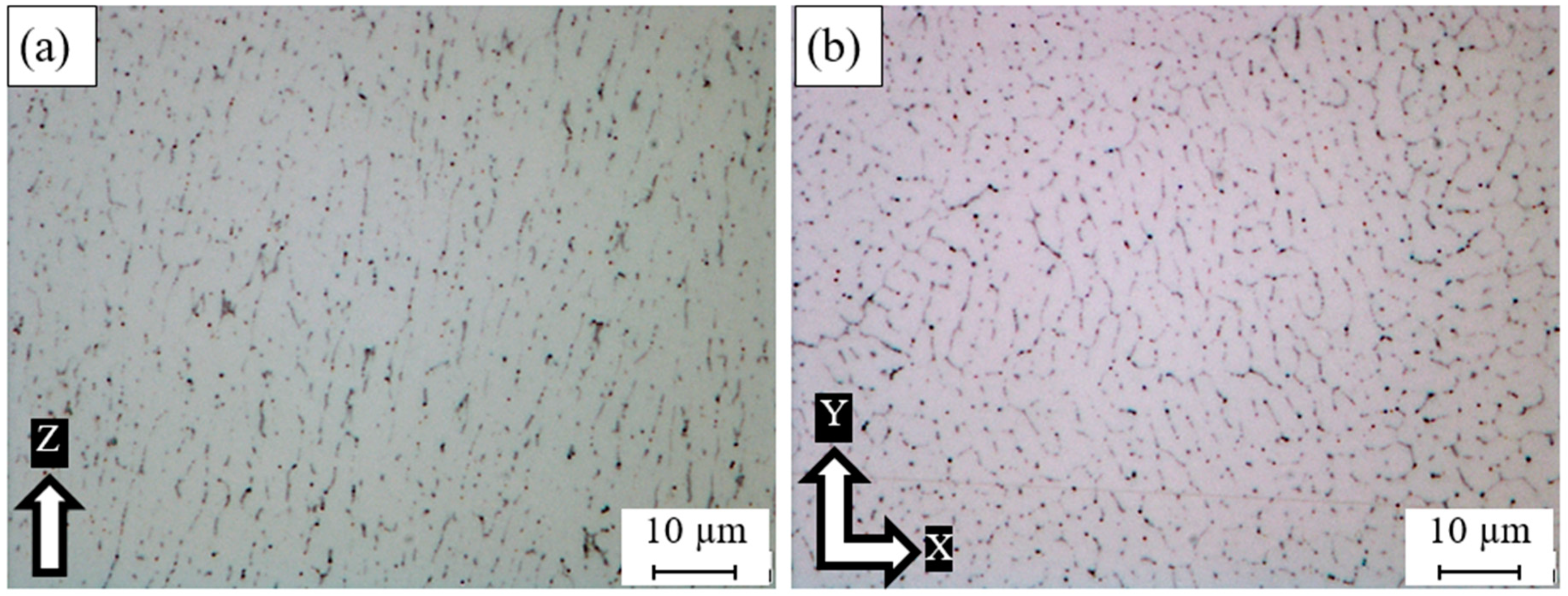
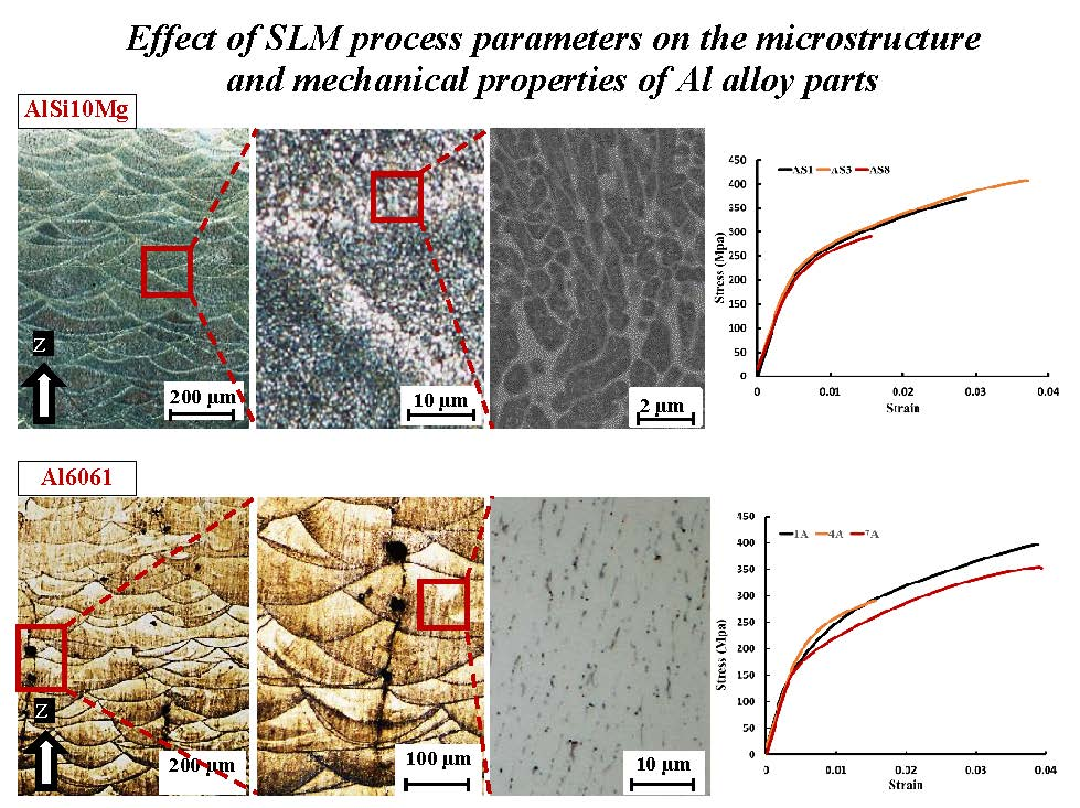
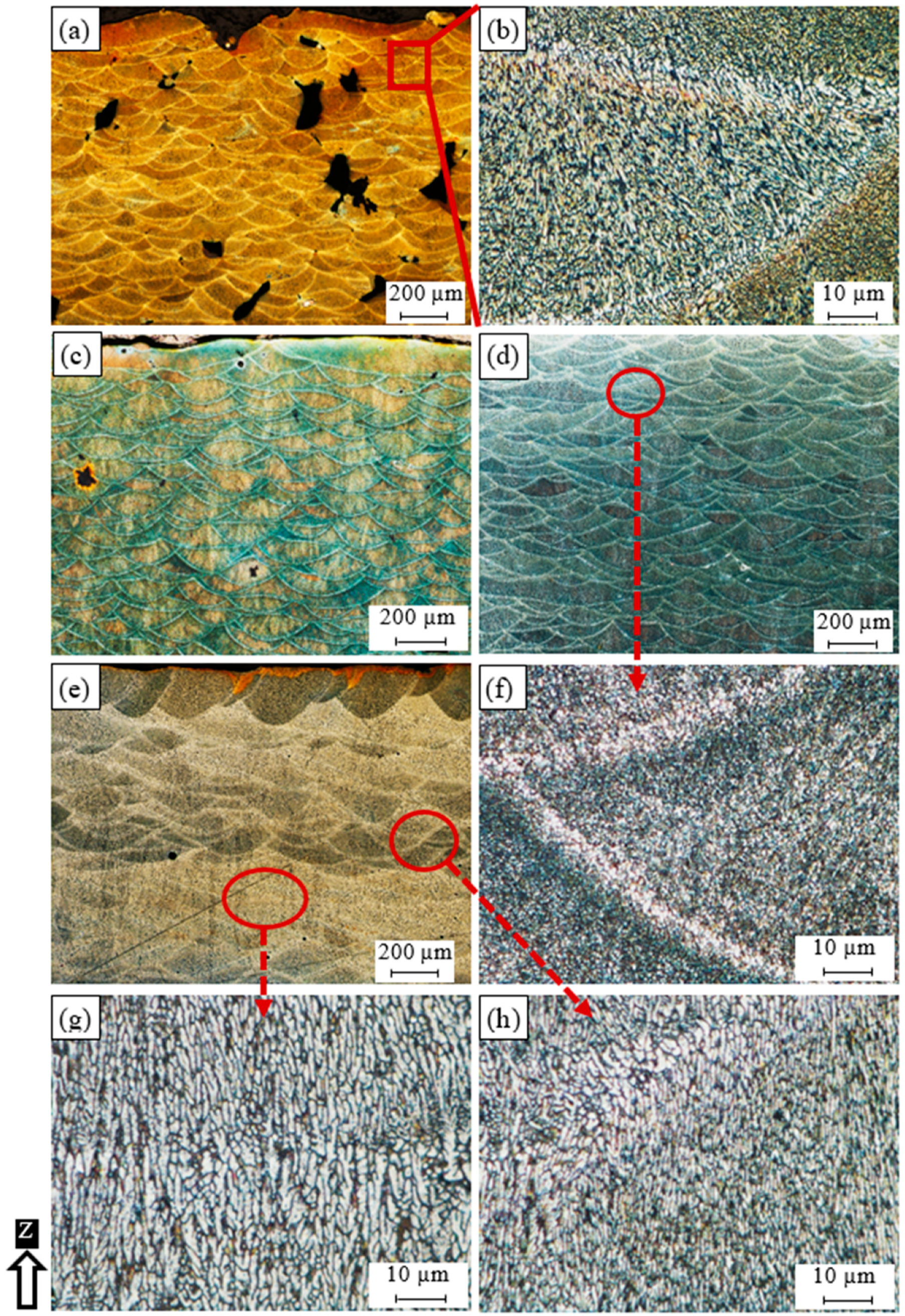
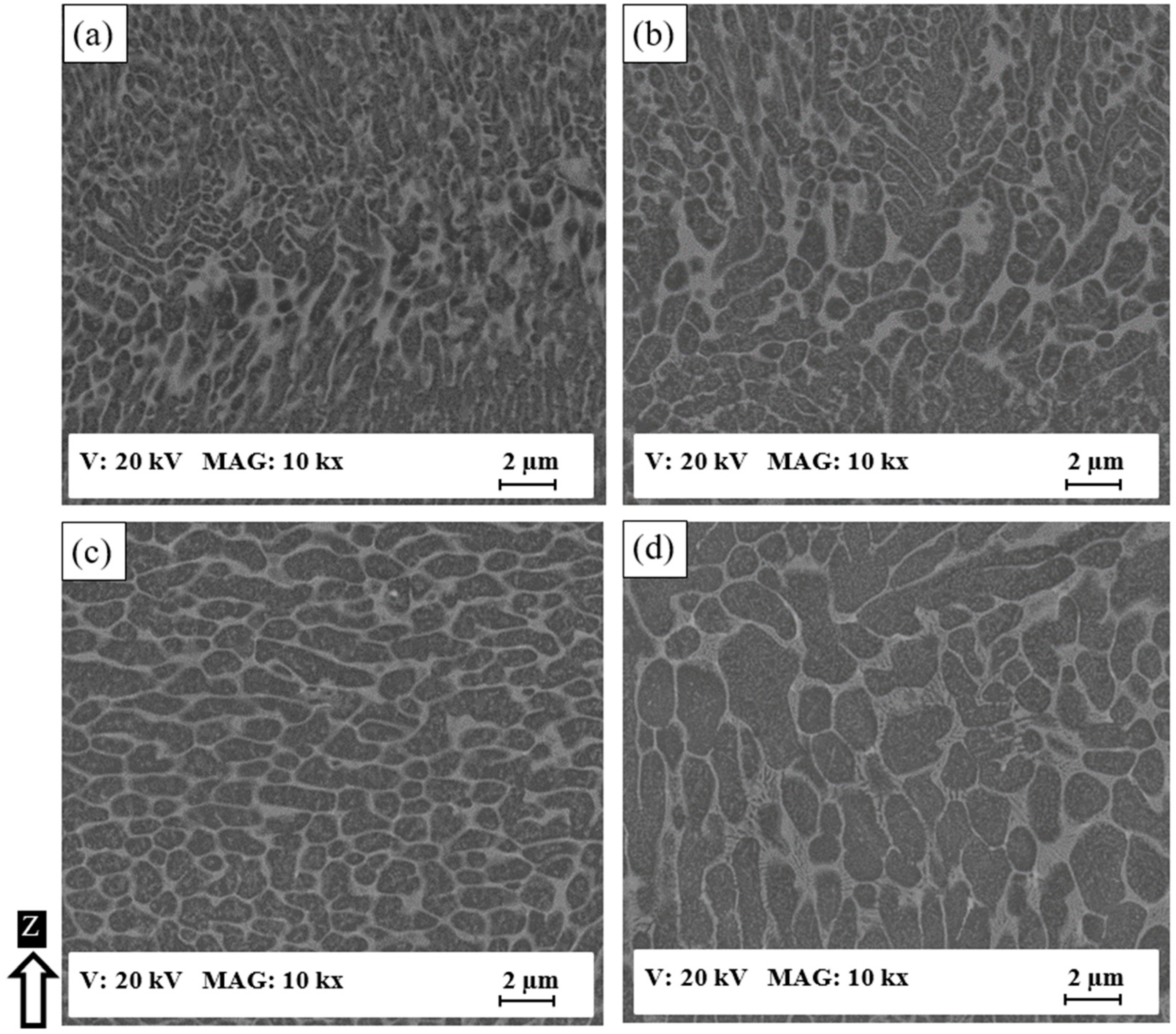
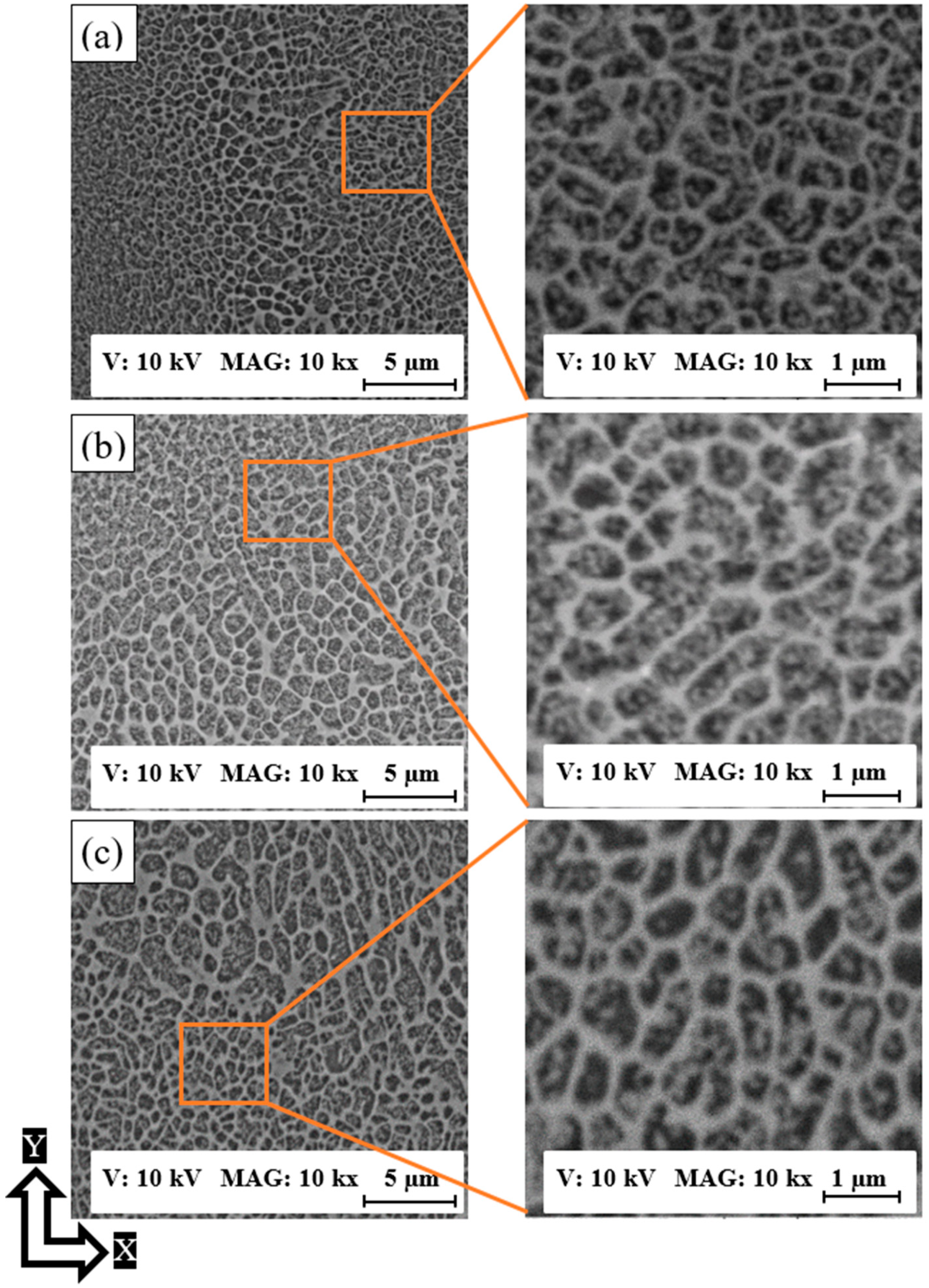
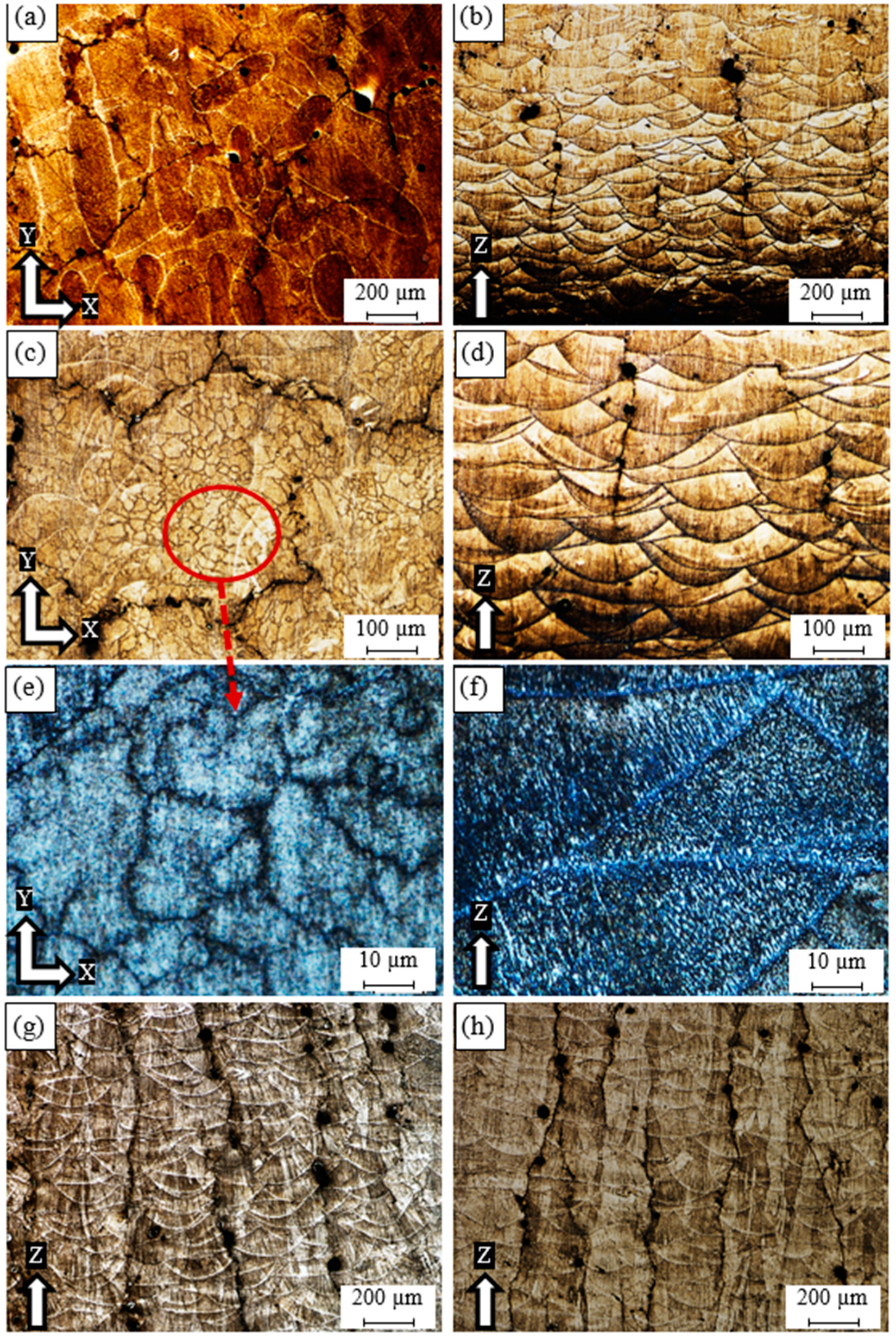
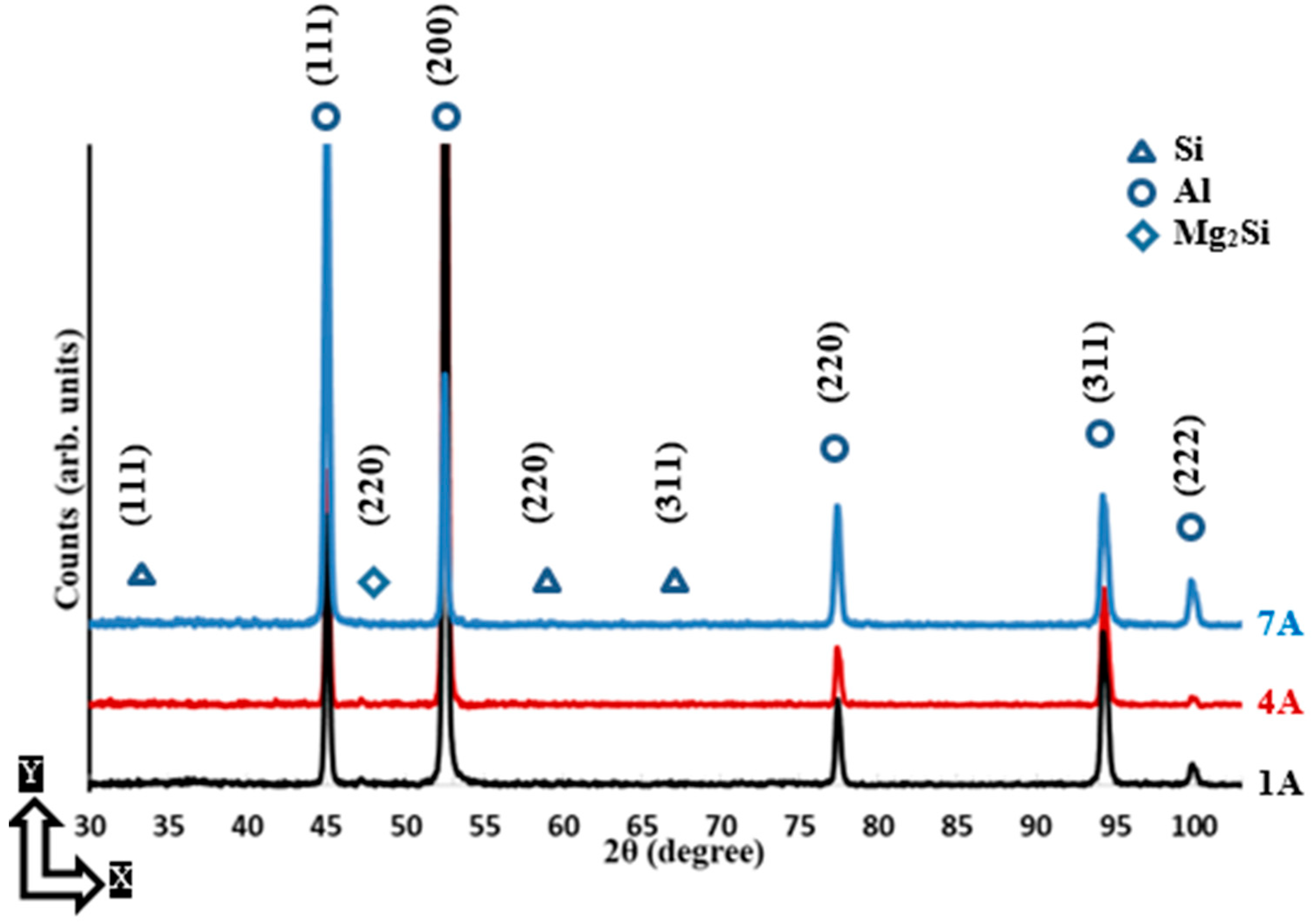
3.1. Microstructure
3.2. Mechanical Properties
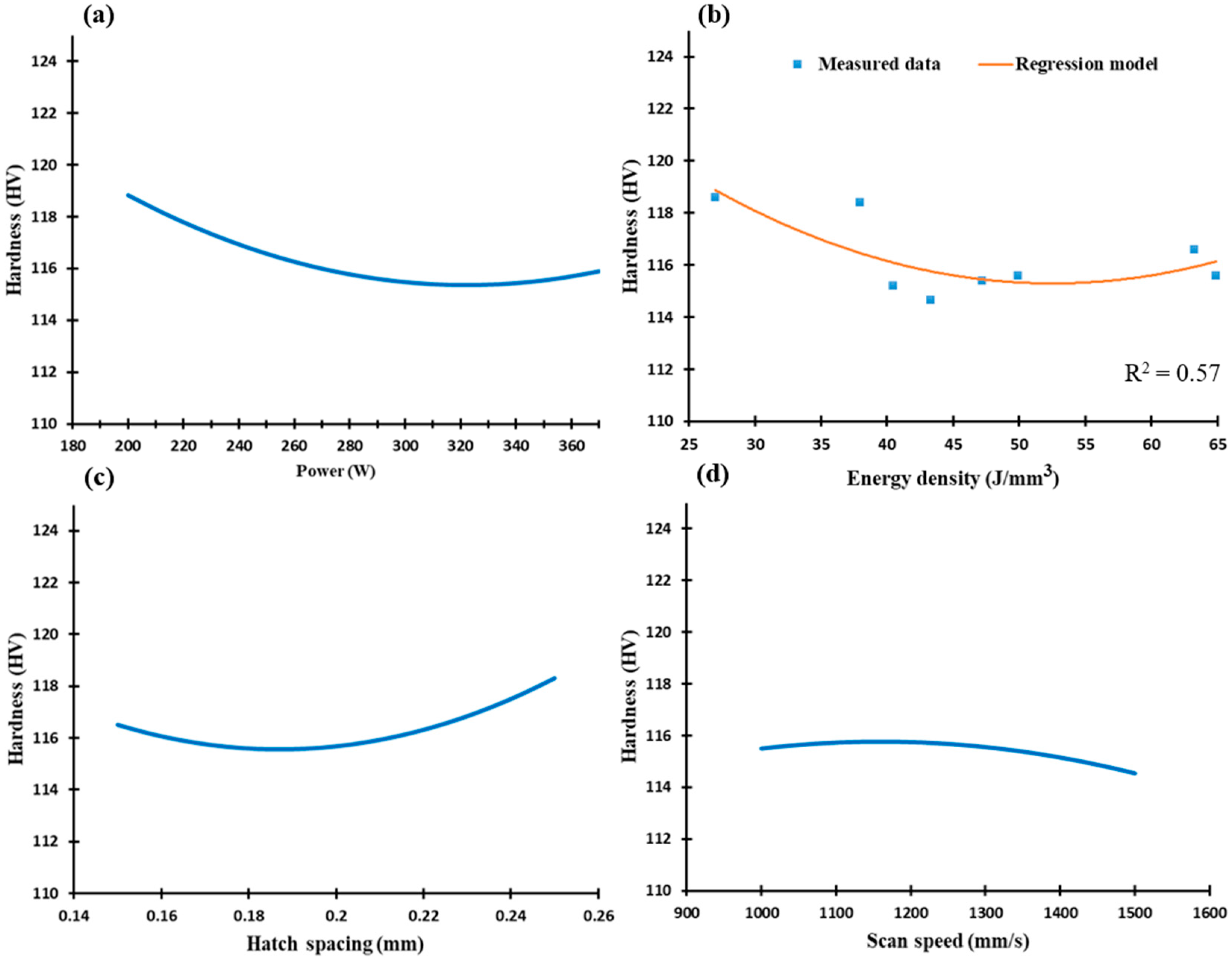
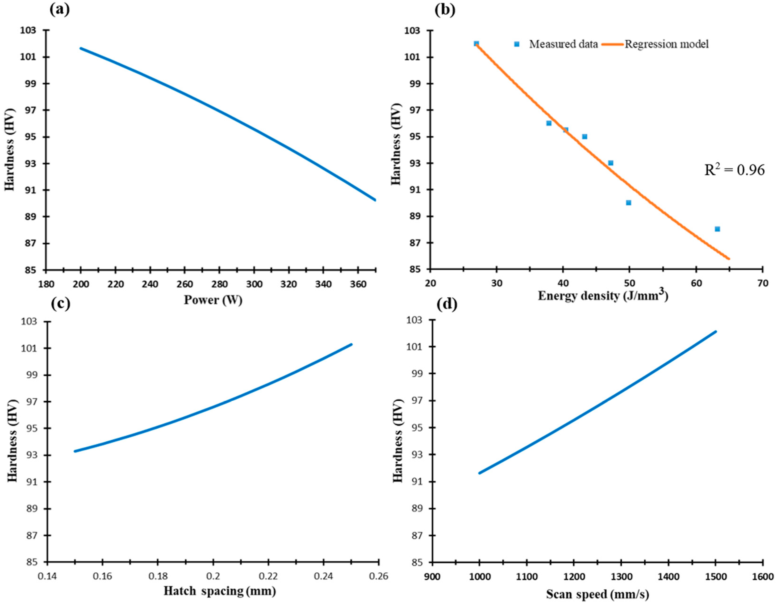
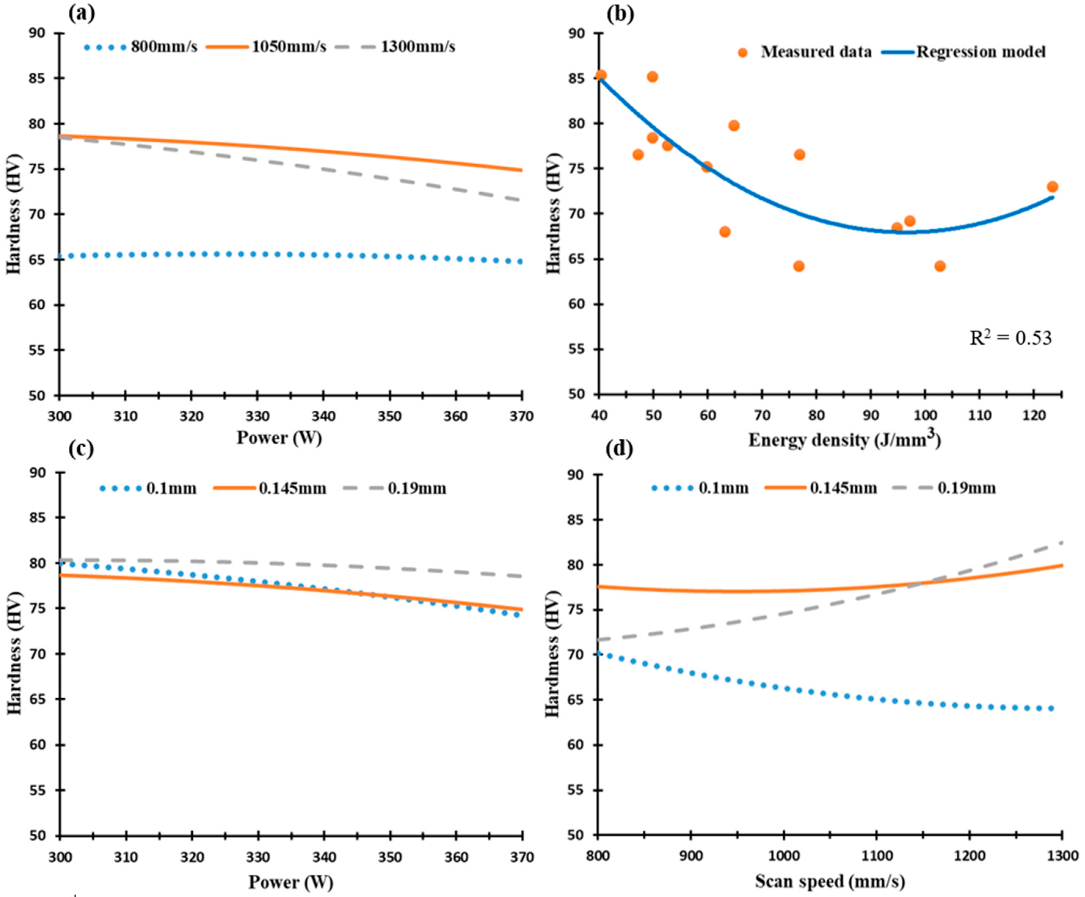
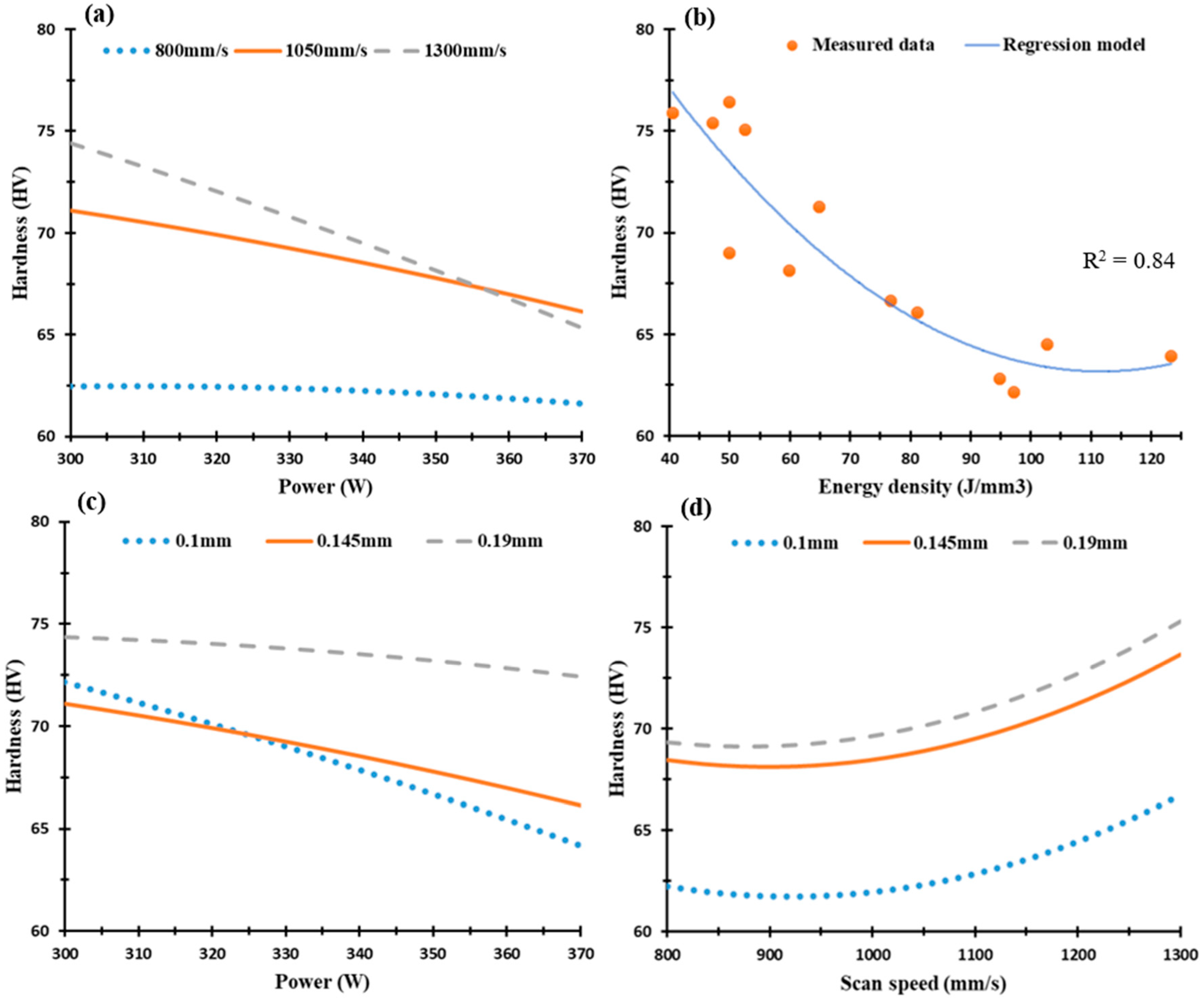
3.2.1. Microhardness
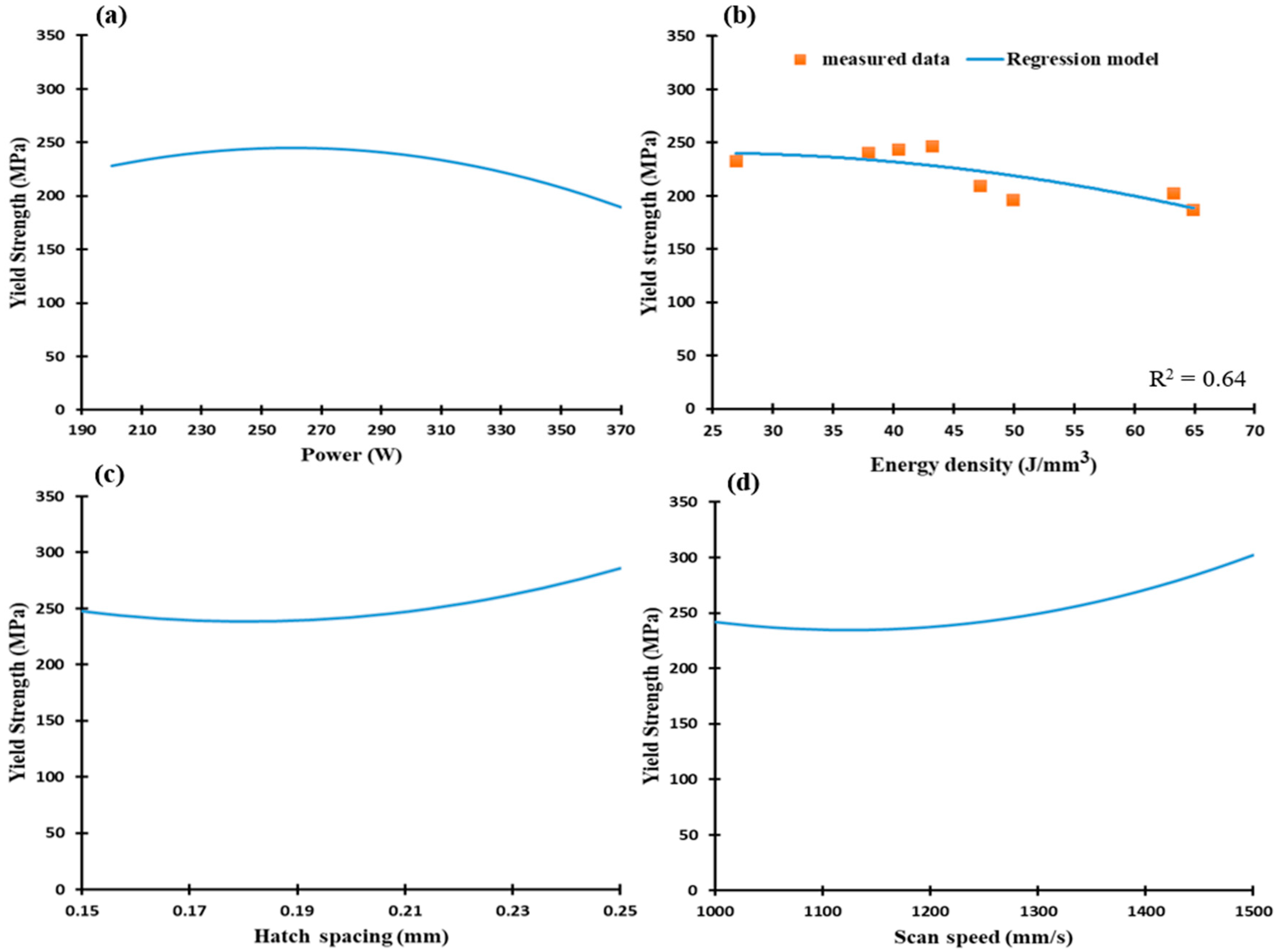
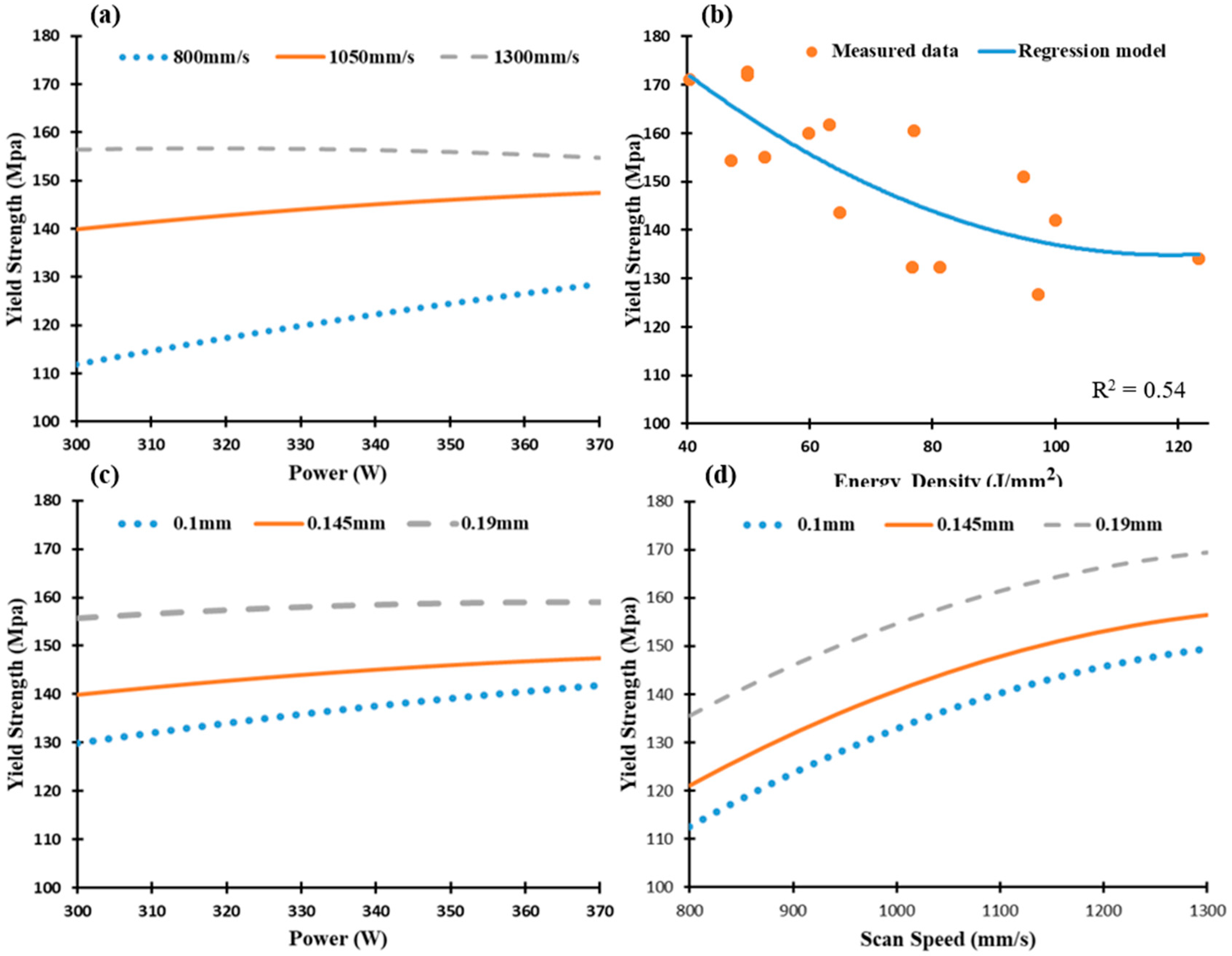
3.2.2. Tensile Properties
4. Summary and Conclusions
Author Contributions
Acknowledgments
Conflicts of Interest
References
- Schwab, K. The Fourth Industrial Revolution; Crown Business: New York, NY, USA, 2017. [Google Scholar]
- Gibson, I.; Rosen, D.; Stucker, B. Development of Additive Manufacturing Technology. In Additive Manufacturing Technologies; Springer: New York, NY, USA, 2015; pp. 19–42. ISBN 978-1-4939-2112-6. [Google Scholar]
- DebRoy, T.; Wei, H.L.; Zuback, J.S.; Mukherjee, T.; Elmer, J.W.; Milewski, J.O.; Beese, A.M.; Wilson-Heid, A.; De, A.; Zhang, W. Additive manufacturing of metallic components—Process, structure and properties. Prog. Mater. Sci. 2018, 92, 112–224. [Google Scholar] [CrossRef]
- Buchbinder, D.; Meiners, W.; Pirch, N.; Wissenbach, K.; Schrage, J. Investigation on reducing distortion by preheating during manufacture of aluminum components using selective laser melting. J. Laser Appl. 2014, 26, 012004. [Google Scholar] [CrossRef]
- Tradowsky, U.; White, J.; Ward, R.M.; Read, N.; Reimers, W.; Attallah, M.M. Selective laser melting of AlSi10Mg: Influence of post-processing on the microstructural and tensile properties development. Mater. Des. 2016, 105, 212–222. [Google Scholar] [CrossRef]
- Olakanmi, E.O.; Cochrane, R.F.; Dalgarno, K.W. A review on selective laser sintering/melting (SLS/SLM) of aluminium alloy powders: Processing, microstructure, and properties. Prog. Mater. Sci. 2015, 74, 401–477. [Google Scholar] [CrossRef] [Green Version]
- Siddique, S.; Imran, M.; Wycisk, E.; Emmelmann, C.; Walther, F. Influence of process-induced microstructure and imperfections on mechanical properties of AlSi12 processed by selective laser melting. J. Mater. Process. Technol. 2015, 221, 205–213. [Google Scholar] [CrossRef]
- Biffi, C.A.; Fiocchi, J.; Tuissi, A. Selective laser melting of AlSi10Mg: Influence of process parameters on Mg2Si precipitation and Si spheroidization. J. Alloys Compd. 2018, 755, 100–107. [Google Scholar] [CrossRef]
- Krishnan, M.; Atzeni, E.; Canali, R.; Calignano, F.; Manfredi, D.; Ambrosio, E.P.; Iuliano, L. On the effect of process parameters on properties of AlSi10Mg parts produced by DMLS. Rapid Prototyp. J. 2014, 20, 449–458. [Google Scholar] [CrossRef]
- Prashanth, K.G.; Scudino, S.; Eckert, J. Defining the tensile properties of Al-12Si parts produced by selective laser melting. Acta Mater. 2017, 126, 25–35. [Google Scholar] [CrossRef]
- Li, W.; Li, S.; Liu, J.; Zhang, A.; Zhou, Y.; Wei, Q.; Yan, C.; Shi, Y. Effect of heat treatment on AlSi10Mg alloy fabricated by selective laser melting: Microstructure evolution, mechanical properties and fracture mechanism. Mater. Sci. Eng. A 2016, 663, 116–125. [Google Scholar] [CrossRef]
- Akram, J.; Chalavadi, P.; Pal, D.; Stucker, B. Understanding grain evolution in additive manufacturing through modeling. Addit. Manuf. 2018, 21, 255–268. [Google Scholar] [CrossRef]
- Fulcher, B.A.; Leigh, D.K.; Watt, T.J. Comparison of AlSi10Mg and Al 6061 Processed Through DMLS. In Proceedings of the Solid Freeform Fabrication (SFF) Symposium, Austin, TX, USA, 4–6 August 2014; pp. 404–419. [Google Scholar]
- Uddin, S.Z.; Murr, L.E.; Terrazas, C.A.; Morton, P.; Roberson, D.A.; Wicker, R.B. Processing and characterization of crack-free aluminum 6061 using high-temperature heating in laser powder bed fusion additive manufacturing. Addit. Manuf. 2018, 22, 405–415. [Google Scholar] [CrossRef]
- Martin, J.H.; Yahata, B.D.; Hundley, J.M.; Mayer, J.A.; Schaedler, T.A.; Pollock, T.M. 3D printing of high-strength aluminium alloys. Nature 2017, 549, 365–369. [Google Scholar] [CrossRef] [PubMed]
- Maamoun, A.; Xue, Y.; Elbestawi, M.; Veldhuis, S. Effect of Selective Laser Melting Process Parameters on the Quality of Al Alloy Parts: Powder Characterization, Density, Surface Roughness, and Dimensional Accuracy. Materials 2018, 11, 2343. [Google Scholar] [CrossRef] [PubMed]
- Tan, J.H.; Wong, W.L.E.; Dalgarno, K.W. An overview of powder granulometry on feedstock and part performance in the selective laser melting process. Addit. Manuf. 2017, 18, 228–255. [Google Scholar] [CrossRef]
- Maamoun, A.H.; Elbestawi, M.; Dosbaeva, G.K.; Veldhuis, S.C. Thermal Post-processing of AlSi10Mg parts produced by Selective Laser Melting using recycled powder. Addit. Manuf. 2018, 21, 234–247. [Google Scholar] [CrossRef]
- Sames, W.J.; List, F.A.; Pannala, S.; Dehoff, R.R.; Babu, S.S. The metallurgy and processing science of metal additive manufacturing. Int. Mater. Rev. 2016, 61, 315–360. [Google Scholar] [CrossRef]
- Liu, Y.J.; Liu, Z.; Jiang, Y.; Wang, G.W.; Yang, Y.; Zhang, L.C. Gradient in microstructure and mechanical property of selective laser melted AlSi10Mg. J. Alloys Compd. 2018, 735, 1414–1421. [Google Scholar] [CrossRef]
- Prashanth, K.G.; Eckert, J. Formation of metastable cellular microstructures in selective laser melted alloys. J. Alloys Compd. 2017, 707, 27–34. [Google Scholar] [CrossRef]
- Maamoun, A.H.; Veldhuis, S.C.; Elbestawi, M. Friction stir processing of AlSi10Mg parts produced by selective laser melting. J. Mater. Process. Technol. 2019, 263, 308–320. [Google Scholar] [CrossRef]
- Maamoun, A.; Elbestawi, M.; Veldhuis, S. Influence of Shot Peening on AlSi10Mg Parts Fabricated by Additive Manufacturing. J. Manuf. Mater. Process. 2018, 2, 40. [Google Scholar] [CrossRef]
- Hooper, P.A. Melt pool temperature and cooling rates in laser powder bed fusion. Addit. Manuf. 2018, 22, 548–559. [Google Scholar] [CrossRef]
- Langford, J.I.; Wilson, A.J.C. Scherrer after sixty years: A survey and some new results in the determination of crystallite size. J. Appl. Crystallogr. 1978, 11, 102–113. [Google Scholar] [CrossRef] [Green Version]
- Prevey, P.S. X-ray Diffraction Characterisation of Residual Stresses Produced by Shot Peening. In Shot Peening Theory and Application; Niku-Lari, A., Ed.; IITT-International: Paris, France, 1990; pp. 81–93. [Google Scholar]
- Carter, L.N.; Attallah, M.M.; Reed, R.C. Laser Powder Bed Fabrication of Nickel-Base Superalloys: Influence of Parameters; Characterisation, Quantification and Mitigation of Cracking. In Superalloys; Huron, E.S., Reed, R.C., Hardy, M.C., Mills, M.J., Montero, R.E., Portella, P.D., Telesman, J., Eds.; TMS: Pittsburgh, PA, USA, 2012; pp. 577–586. ISBN 9780470943205. [Google Scholar]
- Kaufman, J.G.; Rooy, E.L. Aluminum Alloy Castings: Properties, Processes, and Applications; ASM International: Novelty, OH, USA, 2004; ISBN 0871708035. [Google Scholar]
- Ding, Y.; Muñiz-Lerma, J.A.; Trask, M.; Chou, S.; Walker, A.; Brochu, M. Microstructure and mechanical property considerations in additive manufacturing of aluminum alloys. MRS Bull. 2016, 41, 745–751. [Google Scholar] [CrossRef]
- Kempen, K.; Thijs, L.; Van Humbeeck, J.; Kruth, J.P. Mechanical Properties of AlSi10Mg Produced by Selective Laser Melting. Phys. Procedia 2012, 39, 439–446. [Google Scholar] [CrossRef]
- Read, N.; Wang, W.; Essa, K.; Attallah, M.M. Selective laser melting of AlSi10Mg alloy: Process optimisation and mechanical properties development. Mater. Des. 2015, 65, 417–424. [Google Scholar] [CrossRef]
- Zia Uddin, S.; Espalin, D.; Mireles, J.; Morton, P.; Terrazas, C.; Collins, S.; Murr, L.E.; Wicker, R. Laser powder bed fusion fabrication and characterization of crack-free aluminum alloy 6061 using in-process powder bed induction heating. In Proceedings of the 28th Annual International Solid Freeform Fabrication Symposium, Austin TX, USA, 7–9 August 2017; pp. 214–227. [Google Scholar]
- Material Data Sheet: EOS Aluminium AlSi10Mg; EOS GmbH-Electro Optical Systems: Krailling, Germany, 2014.
- Material Data Sheet: EOS Aluminium AlSi10Mg_200C; EOS GmbH-Electro Optical Systems: Krailling, Germany, 2013.
- Raus, A.A.; Wahab, M.S.; Ibrahim, M.; Kamarudin, K.; Ahmed, A.; Shamsudin, S. Mechanical and Physical Properties of AlSi10Mg Processed through Selective Laser Melting. Int. J. Eng. Technol. 2016, 8, 2612–2618. [Google Scholar] [CrossRef]
- Buchbinder, D.; Meiners, W. Generative Fertigung von Aluminiumbauteilen für die Serienproduktion; Fraunhofer Institute: Aachen, Germany, 2010. [Google Scholar]
- Lumley, R.N. Technical Data Sheets for Heat-Treated Aluminum High-Pressure Die Castings. Die Cast. Eng. 2008, 52, 32–36. [Google Scholar]
- Metals, A.S. Properties and Selection: Nonferrous Alloys and Special-Purpose Materials; American Society for Metals: Geauga, OH, USA, 1990; ISBN 0871703785. [Google Scholar]


| Sample | P (W) | Vs (mm/s) | Dh (mm) | Ed (J/mm3) |
|---|---|---|---|---|
| AS1 | 370 | 1000 | 0.19 | 65 |
| AS2 | 370 | 1300 | 0.15 | 63.2 |
| AS3 | 370 | 1300 | 0.19 | 50 |
| AS4 | 350 | 1300 | 0.19 | 47.2 |
| AS5 | 370 | 1500 | 0.19 | 43.3 |
| AS6 | 300 | 1300 | 0.19 | 40.5 |
| AS7 | 370 | 1300 | 0.25 | 38 |
| AS8 | 200 | 1300 | 0.19 | 27 |
| Sample | P (W) | Vs (mm/s) | Dh (mm) | Ed (J/mm3) | Sample | P (W) | Vs (mm/s) | Dh (mm) | Ed (J/mm3) |
|---|---|---|---|---|---|---|---|---|---|
| 1A | 370 | 1000 | 0.1 | 123.3 | 11A | 370 | 800 | 0.15 | 102.8 |
| 2A | 300 | 1000 | 0.1 | 100 | 12A | 350 | 800 | 0.15 | 97.2 |
| 3A | 370 | 1300 | 0.1 | 95 | 13A | 370 | 800 | 0.19 | 81.1 |
| 4A | 300 | 1300 | 0.1 | 76.9 | 14A | 350 | 800 | 0.19 | 76.8 |
| 5A | 370 | 1000 | 0.19 | 65 | 15A | 370 | 1300 | 0.15 | 63.2 |
| 6A | 300 | 1000 | 0.19 | 52.6 | 16A | 350 | 1300 | 0.15 | 59.8 |
| 7A | 370 | 1300 | 0.19 | 50 | 17A | 370 | 1300 | 0.19 | 50 |
| 8A | 300 | 1300 | 0.19 | 40.5 | 18A | 350 | 1300 | 0.19 | 47.2 |
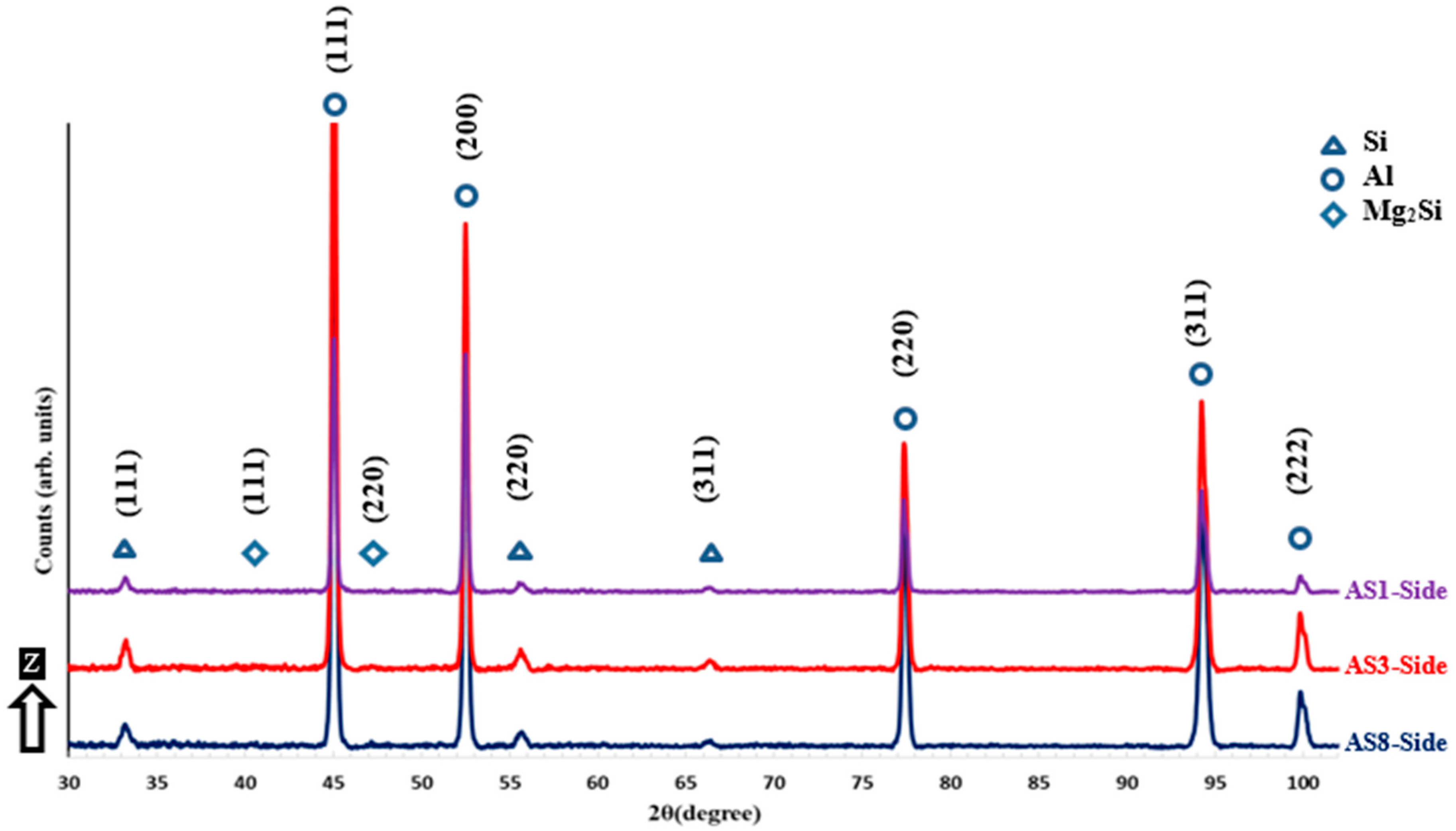
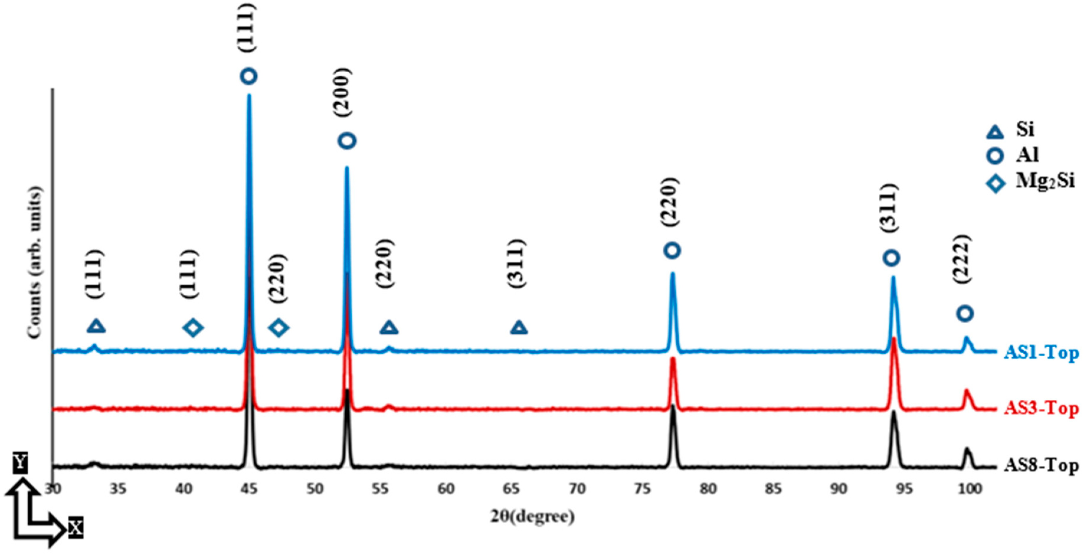
| Material | Peak | Position | AS1 | AS3 | AS8 |
|---|---|---|---|---|---|
| AlSi10Mg | Al (200) FWHM (°) | Top (XY) | 0.2111 | 0.2332 | 0.2294 |
| Side (Z) | 0.2105 | 0.2304 | 0.2269 | ||
| Si (220) FWHM (°) | Top (XY) | 0.5935 | 0.7281 | 0.7137 | |
| Side (Z) | 0.5217 | 0.5531 | 0.5420 |
| Material | Element | Top Surface (XY plane) | Side Surface (Z-direction) | ||||
|---|---|---|---|---|---|---|---|
| AS1 | AS3 | AS8 | AS1 | AS3 | AS8 | ||
| AlSi10Mg | Al wt.% | 91.11 | 91.98 | 90.81 | 93.49 | 93.57 | 90.75 |
| Si wt.% | 8.89 | 8.02 | 9.19 | 6.51 | 6.43 | 9.25 | |
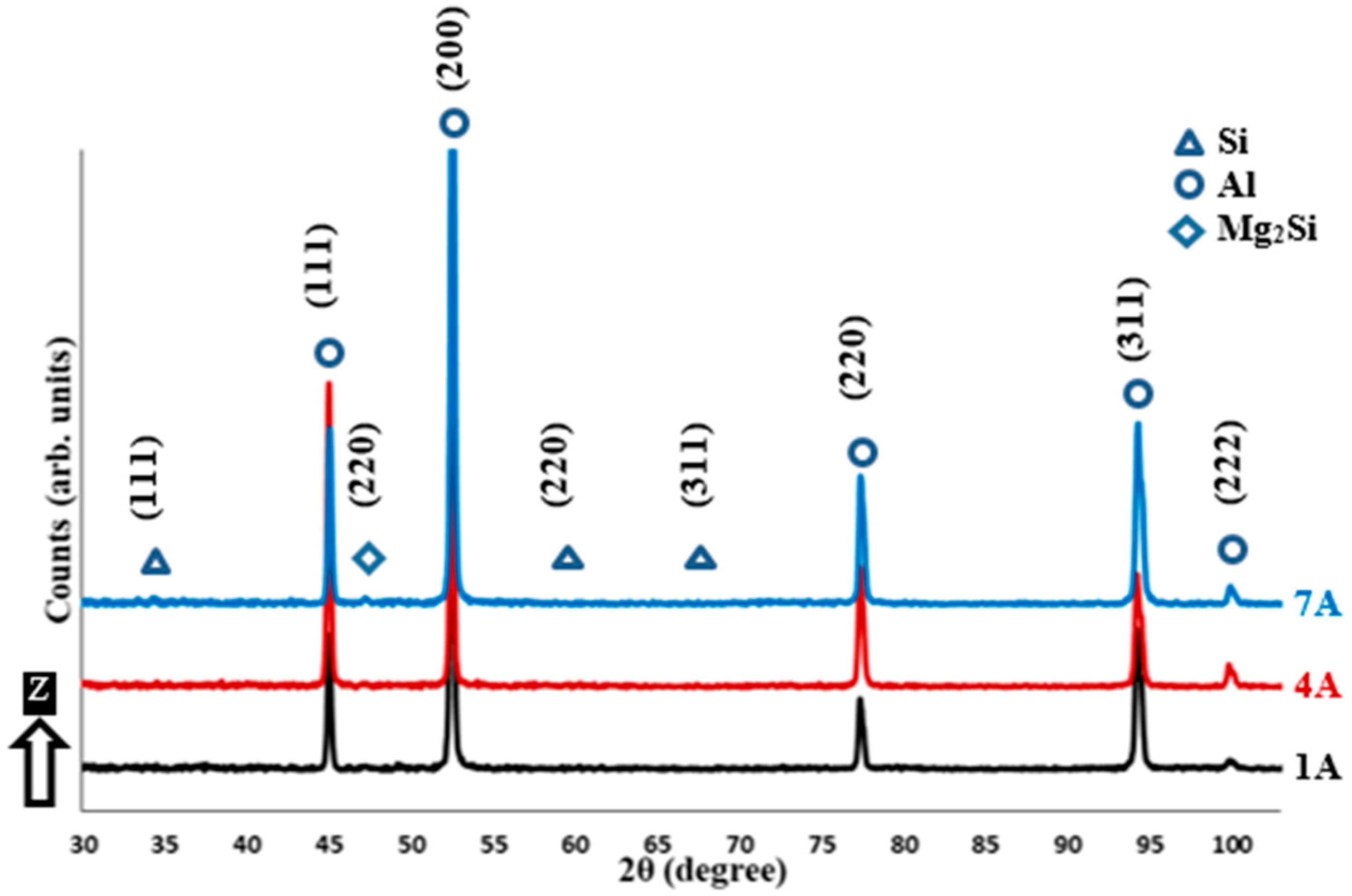
| Material | Peak | Position | 1A | 4A | 7A |
|---|---|---|---|---|---|
| Al6061 | Al (200) FWHM (°) | Top (XY) | 0.1874 | 0.2086 | 0.2045 |
| Side (Z) | 0.1838 | 0.2042 | 0.2029 |
| Material | SLM Process Parameters | Energy Density (J/mm3) | Treatment | UTS (MPa) | Yield Strength (MPa) | Average Hardness (HV) | Al Matrix Grain Size (µm) | ||
|---|---|---|---|---|---|---|---|---|---|
| P (W) | Vs (mm/s) | Dh (mm) | |||||||
| AlSi10Mg_200C (Current Study) | 370 | 1000 | 0.19 | 65 | As-built | 354.6 | 186.4 | Z 102 | 3–4 |
| XY 118 | 0.3–2 | ||||||||
| 370 | 1300 | 0.19 | 50 | As-built | 396.5 | 196 | Z 90 | 0.5–3 | |
| XY 115 | 0.3–2 | ||||||||
| 200 | 1300 | 0.19 | 27 | As-built | 290.6 | 232.3 | Z 84.5 | 0.2–2 | |
| XY 116 | 0.15–1 | ||||||||
| AlSi10Mg_200C [18] | 370 | 1300 | 0.19 | 50 | As-built | Z 120 | 0.5–1 | ||
| XY 130 | |||||||||
| T6 | Z 115 | 1–5 | |||||||
| XY 116 | |||||||||
| AlSi10Mg [36] | 250 | 500 | 0.5 | As-built | 350 | 250 | 145 | ||
| T6 | 285 | 340 | 116 | ||||||
| AlSi10Mg [33] | As-built | 460 ± 20 | 270 ± 10 | 119 ± 5 | |||||
| AlSi10Mg_200C [34] | As-built | 390 | 210 | ||||||
| AlSi10Mg [30] | 200 | 1400 | 0.105 | As-built | 391 ± 6 | 127 | |||
| AlSi10Mg [35] | 350 | 1650 | 0.13 | 54.4 | As-built | 412 ± 2 | 242 ± 5 | 139 | |
| AlSi10Mg [37] | HPDC | 300–350 | 160–185 | 95–105 | |||||
| HPDC-T6 | 330–365 | 285–330 | 130–133 | ||||||
| A360 [28] | Casting | 317 | 165 | 75 | |||||
| Al6061_200C (Current Study) | 370 | 1000 | 0.1 | 123.3 | As-built | 396.5 | 196 | Z 67 | 4–6 |
| XY 71 | 4–5 | ||||||||
| 300 | 1300 | 0.1 | 76.9 | As-built | 290 | 232.3 | Z 81 | 4–5 | |
| XY 77 | 3–4 | ||||||||
| 370 | 1300 | 0.19 | 50 | As-built | 392 | 246.7 | Z 67 | 3–5 | |
| XY 84 | 2–4 | ||||||||
| Al6061 [14,32] | 400 | 1400 | 0.14 | 20.41 | As-built | 90 ± 6 | |||
| Al6061_500C [14] | As-built | 133 | 66 | 54 ± 2.5 | |||||
| T6 | 308 | 282 | 119 ± 6 | ||||||
| AA6061-wrought [38] | O | 125 | 55 | 30 | |||||
| T4 | 240 | 145 | 65 | ||||||
| T6 | 310 | 276 | 95 | ||||||
© 2018 by the authors. Licensee MDPI, Basel, Switzerland. This article is an open access article distributed under the terms and conditions of the Creative Commons Attribution (CC BY) license (http://creativecommons.org/licenses/by/4.0/).
Share and Cite
Maamoun, A.H.; Xue, Y.F.; Elbestawi, M.A.; Veldhuis, S.C. The Effect of Selective Laser Melting Process Parameters on the Microstructure and Mechanical Properties of Al6061 and AlSi10Mg Alloys. Materials 2019, 12, 12. https://doi.org/10.3390/ma12010012
Maamoun AH, Xue YF, Elbestawi MA, Veldhuis SC. The Effect of Selective Laser Melting Process Parameters on the Microstructure and Mechanical Properties of Al6061 and AlSi10Mg Alloys. Materials. 2019; 12(1):12. https://doi.org/10.3390/ma12010012
Chicago/Turabian StyleMaamoun, Ahmed H., Yi F. Xue, Mohamed A. Elbestawi, and Stephen C. Veldhuis. 2019. "The Effect of Selective Laser Melting Process Parameters on the Microstructure and Mechanical Properties of Al6061 and AlSi10Mg Alloys" Materials 12, no. 1: 12. https://doi.org/10.3390/ma12010012