Abstract
The formation of high-melting-point Cu6Sn5 interconnections is crucial to overcome the collapse of Sn-based micro-bumps and to produce reliable intermetallic interconnections in three-dimensional (3D) packages. However, because of multiple reflows in 3D package manufacturing, Cu6Sn5 interconnections will experience cyclic polymorphic transitions in the solid state. The repeated and abrupt changes in the Cu6Sn5 lattice due to the cyclic polymorphic transitions can cause extreme strain oscillations, producing damage at the surface and in the interior of the Cu6Sn5 matrix. Moreover, because of the polymorphic transition-induced grain splitting and superstructure phase formation, the reliability of Cu6Sn5 interconnections will thus face great challenges in 3D packages. In addition, the Cu6Sn5 polymorphic transition is structure-dependent, and the η′↔η polymorphic transition will occur at the surface while the η′↔ηs↔η polymorphic transition will occur in the deep matrix. This study can provide in-depth understanding of the structural evolution and damage mechanism of Cu6Sn5 interconnections in real 3D package manufacturing.
1. Introduction
Three-dimensional (3D) packages, which can merge chip technology and packaging technology together, have great application in overcoming the scaling limits in 2D integrated circuits (ICs). The most typical characteristics of this technology are to vertically stack the multi-chips in a tight device space and to continuously minimize the interconnections on a limited chip area. As shown in Figure 1, there are four kinds of solder joints in 3D packages. The ball grid array (BGA) solder joints of 760 µm in diameter are above the printed circuit board (PCB). The controlled collapse chip connection (C4) solder joints of 250 µm in diameter are above the BGA package substrate. The Sn-based micro-bumps (Sn-bumps) of 80 µm in diameter are above the interposer substrate. The Sn-bumps of 20 µm in diameter are located between the stacked chips and through-Si-via (TSV) structures. In 3D packages, the Sn-bumps of 20 µm in diameter must be completely transformed into the intermetallic (IMC) phase in the joints after the first reflow, to avoid joint collapse during multiple reflow processes [1]. Accordingly, the IMCs, e.g., Cu6Sn5, Cu3Sn and Ni3Sn4, are quickly emerging as innovative high-temperature interconnection materials due to their unique abilities to join at low temperatures and operate at high temperatures [2,3,4,5]. Among these IMCs, Cu6Sn5 has received a substantial amount of attention because of its fast growth rate and high-temperature strength [6,7]. Sakuma et al. even concluded that realization of the Cu6Sn5 interconnections may be a guarantee of manufacturability and reliability in 3D packages [8].
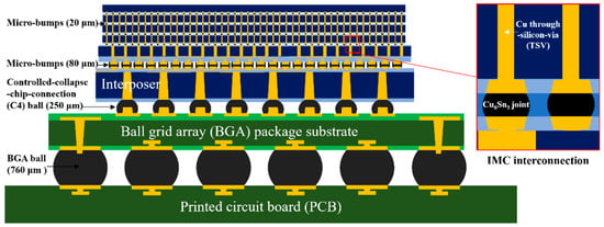
Figure 1.
Schematic illustration of a 3D IC using 3D package technology. IMC = intermetallic phase.
Because of the thermal mismatch between Cu6Sn5 and Si during multiple reflow processes, cyclic strains are considered to be the dominant cause of damage to IMC interconnections in 3D packages [9,10]. However, Cu6Sn5 has at least two phases in the solid state, and its η phase (P63/mmc) can thermodynamically transform to the η′ phase (C2/c) with a volume expansion of 2.2% below 186 °C [11,12]. Because small joints have elevated heating/cooling rates, the polymorphic transition of η′↔η may be kinetically retarded owing to the insufficient transition time. It is concerning that this retarded polymorphic transition may cause a transition stress that continuously damages the Cu6Sn5 IMC interconnection [13,14]. Although some researchers have begun to explore the effect of the Cu6Sn5 polymorphic transition on the interconnect reliability [14,15,16], the intrinsic damage mechanism has seldom been reported during multiple reflow processes. On 7 October, 2019, Samsung Electronics announced that it had developed the industry’s first 12-layer-3D-IC, and that the IMC interconnections in such 3D IC may experience over 10 reflow cycles. Because the number of stacking layers will never end, a 50-layer 3D IC may be fabricated in the near future, and the IMC interconnections in such 3D IC may experience 50 or even more reflow cycles. Therefore, the determination of the damage mode of Cu6Sn5 during multiple reflow processes is urgent in real 3D package manufacturing. The aims of this study were to explore the structural evolution of the Cu6Sn5 under multiple reflow processes, to study the damage mechanism induced by the cyclic polymorphic transitions, and to confirm the influence of cyclic polymorphic transitions on the reliability of Cu6Sn5 interconnections in 3D package manufacturing.
2. Materials and Methods
The Cu6Sn5 IMCs were separated via a precipitation method from a supersaturated Sn–Cu melt [17]. To be specific, a solder bath containing 1 kg of the Sn-0.7 wt% Cu solder and 30 g of the fine Cu powder was placed in a furnace, heated to 350 °C for 24 h under N2 atmosphere. After the Cu powder was completely dissolved, the solder was quickly cooled down to 250 °C and maintained at this temperature for 10 h. Several rod-type IMCs were then separated from this solder using a quartz screen and quenched down to 0 °C. To expose the pure IMCs, the residual solder on their surfaces was etched by a 10% hydrochloric acid alcohol solution.
Subsequently, the as-prepared IMCs were reflowed under a ramp-soak-spike profile provided by a BGA rework machine (RD-500II, DEN-ON INSTRUMENTS Inc., Tokyo, Japan). The temperature ranges of the ramp zone, soak zone and spike zone were set at 20–170 °C, 170–200 °C, and 200–220 °C, respectively, with the same ramp rates of 10 °C/min. After heating to 220 °C, the samples were maintained at this temperature for 10 min, and then cooled down to 20 °C with a cooling rate of 20 °C/min. The aforesaid reflow process was repeated 1 time, 10 times, and 50 times.
The structural evaluation of the Cu6Sn5 IMCs after multiple reflows was observed by scanning electron microscopy (SEM, SU-70, Hitachi Inc., Fukuoka, Japan). Moreover, the Cu6Sn5 grains that were reflowed 1 time were milled to obtain a fine powder and studied by X-ray diffraction (XRD, D8 Advance, Bruker Inc., Karlsruhe, Germany, Cu-Kα radiation) and differential scanning calorimetry (DSC, 214 Polyma, NETZSCH Inc., Selb, Germany). It should be noted that the XRD measurement was conducted at a cooling rate of 20 °C/min from 220 °C to 20 °C, and that the data at each selected temperature were collected in the 2θ range of 30°–55° with a scan rate of 1°/min; the DSC measurement was conducted at a heating/cooling rate of 1 °C/min from 20 °C to 220 °C under an air atmosphere, and the sample of ~28 mg was involved. In addition, to study the η′↔η polymorphic transition, two Cu6Sn5 grains that were reflowed 1 time and 50 times, respectively, were cut by a focused-ion beam (FIB, NanoLab 600i, FEI Inc., Hillsboro, OR, USA), and the corresponding microstructures were studied by transmission electron microscopy (TEM, Tecnai G2 F20, Philips Inc., Eindhoven, Holland). It should be noted that Figure 2 shows a flowchart of the preparation, reflow tests, and the characterization of Cu6Sn5 IMCs.
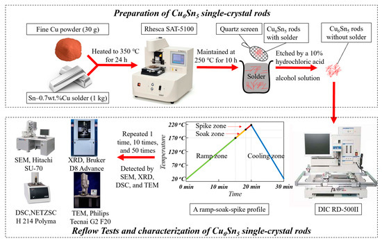
Figure 2.
Flowchart of the preparation, reflow tests and the characterization of Cu6Sn5 IMCs. DSC = differential scanning calorimetry.
3. Results and Discussion
Figure 3 shows the surface evolution of the Cu6Sn5 IMCs with increasing reflow time. After being reflowed 1 time, the Cu6Sn5 grains maintained a rod-like shape with flat and smooth surfaces. The diameters of these grains were in the range of 20–25 µm, and each grain was a single crystal based on the previous study [17]. Interestingly, after being reflowed 10 times, although the overall structures of these IMC grains did not change, the original smooth surfaces became rough and full of microcracks (Figure 3b). After being reflowed 50 times, the Cu6Sn5 surfaces became damaged and fragmented, and numerous protrusion-like structures with irregular shapes and sizes emerged in certain depressed areas (Figure 3c). Apparently, the surface damage of the Cu6Sn5 grains arose after multiple reflows, and the damage extent seemed to increase with the increasing number of reflow times. Hence, we reasonably hypothesize that multiple reflows will produce an adverse effect on the reliability of Cu6Sn5 interconnections in 3D packages. To verify our speculation, the structural changes inside the Cu6Sn5 grains should be further explored.
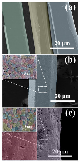
Figure 3.
Surface microstructures of the Cu6Sn5 grains after being reflowed (a) 1 time; (b) 10 times; (c) 50 times.
Figure 4a shows the XRD patterns of the Cu6Sn5 powder after being reflowed 1 time at selected temperatures. The patterns in the temperature range of 20–150 °C are roughly identical, and by comparing the peak positions and peak intensities with the reference database, it is concluded that the corresponding main diffraction peaks are attributable to the η′ phase (International Centre for Diffraction Data (ICDD) 45-1488, space group of C2/c). The XRD patterns in the temperature range of 170–220 °C are similar, and the corresponding main diffraction peaks are attributable to the η phase (ICDD 47-1575, space group of P63/mmc). Moreover, there are numerous relatively weak peaks at 2θ values of 32.35°, 39.48°, 48.39° and 49.84° for the patterns in the temperature range of 20–150 °C (marked by the dark-blue squares) and at 2θ values of 38.50°, 46.12° and 47.43° for the patterns in the temperature range of 170–220 °C (marked by the red circles), which cannot be well matched to the standard XRD files of the Cu6Sn5. Because superstructures may be created in the Cu6Sn5 during the polymorphic transition of η′↔η [12], these peaks are very likely structural in origin. In addition, in the 2θ range of 42°–44°, there are two main diffraction peaks (at ~42.82° and ~43.32°) for the patterns in the temperature range of 170–220 °C, but one (at ~42.82°) gradually disappears at decreasing temperatures of 20–150 °C. The main diffraction peaks have fundamentally changed, implying that a reconfiguration of the Cu6Sn5 orientations may occur after the η′↔η polymorphic transition.
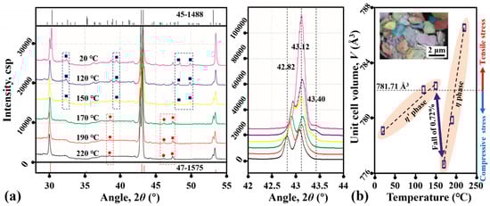
Figure 4.
(a) In situ XRD patterns of the 1-time-reflow Cu6Sn5 powder in the 2θ range of 30°–55°; (b) the calculated unit cell volume (V) at selected temperatures. Note that the monoclinic structure of ICDD 45-1488 is used to fit the pattern in (b), and the microstructures of the Cu6Sn5 powder used in our XRD tests are also inserted in (b).
Figure 4b shows the unit cell volumes of the Cu6Sn5 (V) at selected temperatures calculated from our XRD data. Two almost linear increases in V are detected, with increasing temperatures ranging from 20 to 150 °C and 170 to 220 °C, and a sharp fall of 0.72% occurs from 150 to 170 °C. The former is in accordance with thermal expansions and contractions, and the latter should originate from the Cu6Sn5 polymorphic transition. Because the theoretical value of V is 781.71 Å3, the difference between the theoretical and actual values in V will inevitably produce the tensile/compressive strains inside the Cu6Sn5 lattice. Especially during multiple reflows, a repeated abrupt change in V due to the cyclic polymorphic transitions may cause strain oscillations at the micro level. Moreover, at the macro or meso level, the transition strain may be partially released from the grain surface and be partially accumulated inside the grain matrix. Finally, the oscillation, release and accumulation of the transition strain will produce the structural damage of the Cu6Sn5, leading the Cu6Sn5 grains to crack (Figure 3b) or even break (Figure 3c).
Figure 5 shows the DSC heat flow curves of the Cu6Sn5 powder after being reflowed 1 time. Two endothermic peaks (at ~181.1 °C and ~187.1 °C, respectively) are detected during heating, while two exothermic peaks (at ~148.4 °C and ~162.3 °C, respectively) are detected during cooling. The distribution of the two latent heat peaks in the heating/cooling curve reflects that there should be three phases participating in the process. In other words, besides the η′ and η phases, a new phase (defined as the ηs phase) may be involved in the Cu6Sn5 polymorphic transition, which is consistent with our XRD forecast. Undoubtably, if the ηs phase indeed exists, the first and second latent heat peaks will be related to the η′↔ηs and ηs↔η phase transitions, respectively. Therefore, a single-phase state of the Cu6Sn5 powder during cooling can be predicted: e.g., the η phase at above 170 °C, the ηs phase at close to 150 °C, and the η′ phase at below 140 °C. However, based on our XRD data, the ηs phase seems always to be associated in the η′ or η phase, rather than existing as a separate phase. Hence, an exploration of the existence of the ηs phase is urgently required.
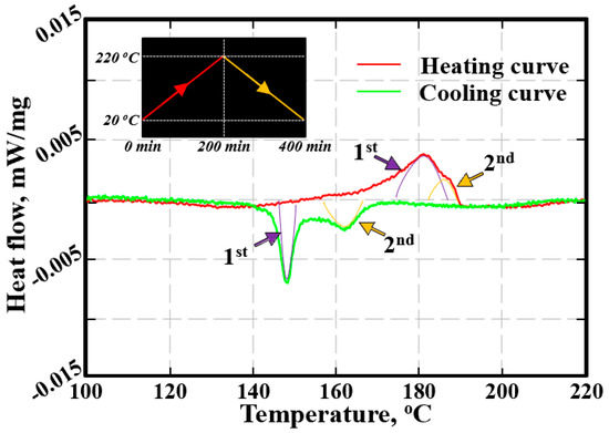
Figure 5.
DSC heat flow curves of the Cu6Sn5 powder after being reflowed 1 time, and the pre-set temperature profile is also included.
Figure 6a shows the cross-section microstructure of a Cu6Sn5 grain after being reflowed 1 time. No grain boundary exists in the Cu6Sn5 matrix, proving that the original rod-type grain before FIB cutting is indeed single-crystal. As shown in Figure 6b, the selected area diffraction pattern (SADP) analysis confirmed that the entire Cu6Sn5 grain is the η′ phase; the normal direction of the matrix is along the [01]η′ direction, and the external surface belongs to the (3)η′ plane. Interestingly, after being reflowed 50 times (Figure 7a), the original Cu6Sn5 single-crystal matrix has split into small grains whose grain boundaries are extended from the external surface to the deep matrix. The grains located close to the external surface (e.g., Grain A and Grain B) seem larger than those located deep inside the matrix (e.g., Grain C and Grain D). Based on the corresponding SADPs in Figure 7b, both Grain A and Grain B are identified as the η′ phase, and a set of orientation relationships are determined as follows: [010]η′-A//[01]η′-B, (02)η′-A//(336)η′-B and (204)η′-A//(12)η′-B. The orientation of Grain B is highly similar to the orientation of the Cu6Sn5 matrix in Figure 6b, but the orientation of Grain A has changed significantly. On the one hand, this indicates that the newly generated grains should originate from the original Cu6Sn5 single-crystal matrix; on the other hand, it demonstrates that the reconfiguration of the Cu6Sn5 orientations has indeed occurred after multiple reflows, at least for certain grains.
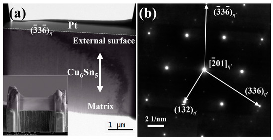
Figure 6.
(a) TEM image of the cross-section microstructure for a rod-type Cu6Sn5 grain after being reflowed 1 time; (b) the corresponding surface area diffraction pattern (SADP) for the matrix. The SEM image of the sample after focused-ion beam (FIB) cutting is also included in (a).
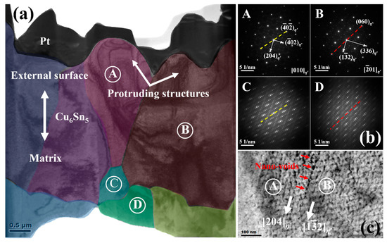
Figure 7.
(a) TEM image of the cross-section microstructure of a rod-type Cu6Sn5 grain reflowed 50 times; (b) the SADPs for the four grains marked in (a); (c) an enlarged view of the local microstructure at the boundary between Grain A and Grain B.
Notably, the theoretical interplanar spacings of the (204)η′, (12)η′, (010)η′ and (01)η′ planes are 2.103 Å, 2.103 Å, 7.294 Å and 5.103 Å, respectively; thus, the lattice mismatch between every one (204)η′ plane and every one (12)η′ plane is 0%, while the potential lattice mismatch between every two (010)η′ planes and every three (01)η′ planes is −4.71%. Despite such small lattice mismatches, some nanovoids are indeed generated at the boundary between Grain A and Grain B after being reflowed 50 times (Figure 7c). Therefore, multiple reflows can indeed result in the damage to inner Cu6Sn5 grains and should be harmful to the reliability of the Cu6Sn5 interconnections in the 3D package. More importantly, as shown in Figure 7b, Grain C has a five-fold superlattice of Grain A running along the [0]η′ direction, while Grain D has a five-fold superlattice of Grain B running along [060]η′. This is direct evidence that a superstructure phase of ηs indeed exists in the Cu6Sn5 matrix, and this finding can perfectly support our speculations in both the XRD and DSC studies.
The formation of the superstructure phase is always strain-induced and structure-dependent (e.g., a strain-induced superstructure phase was observed in ZrCu during the martensitic transition [18]). Following this rule, the formation of the superstructure ηs phase and the mechanism of Cu6Sn5 polymorphic transition can be inferred as below (Figure 8a). When the temperature satisfies the requirement of Cu6Sn5 phase transition, the η′↔η polymorphic transition will begin. Due to the rapid volume change during this transition, the transition strain will inevitably be generated in the Cu6Sn5 lattice; subsequently, such strain will be partially released from the external surface to form a strain-free layer and also be partially accumulated inside the matrix to create a strain-accumulation zone. From the point of view of phase transition energy, the nearer to the surface, the smaller strain energy (i.e., the main resistance to phase transition in solid state) will be, and phase transition is more prone to occur. Hence, the normal η′↔η polymorphic transition can be detected at or close to the external surfaces of the Cu6Sn5 grains, just as observed in Somidin’s in situ heating TEM experiments [11,12]. However, when the strain energy between η′ and η phases is larger than the volume free energy change between η′ and η phases (i.e., the driving force of phase transition), the η′↔η polymorphic transition may stop, and the accumulated strains will promote the metastable phase formation in order to decrease the threshold of η′↔η phase transition. Hence, the η′↔ηs↔η polymorphic transition will occur inside the Cu6Sn5 deep matrix, just as we detected in Figure 7b. Because the ηs phase is metastable and only exists inside the matrix, it can thus be detected in and accompanied by the η′ or η phase, just as shown in Figure 4a.
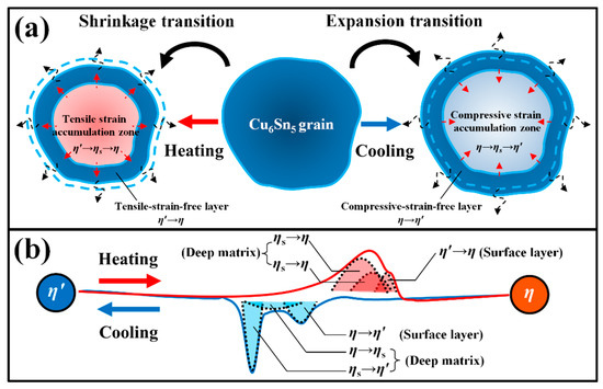
Figure 8.
(a) Sketch map of the structure-induced mechanism of Cu6Sn5 polymorphic transition; (b) the reason for the distribution of latent heat peaks in Cu6Sn5 polymorphic transition.
In addition, because the η→η′ phase transition is an expansion transition, we can infer that the η→ηs→η′ phase transition is also an expansion transition. Based on Figure 4b, the compressive strain will exist in the Cu6Sn5 matrix during cooling below 200 °C; thus, the ηs phase observed in Figure 7b seems to be created only by the compressive strain, and the occurrence of this phase seemed to be in the range of 150–170 °C based on Figure 5. Accordingly, as shown in Figure 8b, the compressive strain generated by the η→η′ expansion transition will create the strain energy inside the matrix, producing the delayed occurrence of the η→ηs expansion transition (i.e., the exothermic peak of η→ηs will shift to the left); similarly, the compressive strain generated by the η→ηs expansion transition may increase the strain energy inside the deep matrix, and the exothermic peak of ηs→η′ will shift further to the left. Therefore, there should be three exothermic peaks involved in the Cu6Sn5 phase transition during the cooling process. Notably, the compressive strain induced by the thermal expansion of the Cu6Sn5 during the heating process will result in a premature occurrence of the η′→ηs→η shrinkage transition; thus, there should also be three endothermic peaks for the Cu6Sn5 phase transition during the heating process. Finally, when the strain is large enough, the splitting of the Cu6Sn5 grains will occur. Accordingly, the strain induced by the cyclic Cu6Sn5 phase transitions is the dominant cause of the crack generation that damages the Cu6Sn5 grains under multiple reflow processes. A further study may verify whether the ηs phase is just one of the η6 phase, η8 phase and η4+1 phase proposed in Nogita’s study [19,20], and evaluate its lattice parameters.
4. Conclusions
The surface and inner structural damage to Cu6Sn5 IMCs after multiple reflow processes was explored in this study. The results show that the superstructure phase formation occurs in Cu6Sn5 due to the accumulation of the strains induced by cyclic phase transitions. Moreover, the nanovoids can be generated at the grain boundaries owing to the lattice mismatch, producing the splitting of the Cu6Sn5 grains after multiple reflows. In addition, the η′↔η polymorphic transition will occur at the Cu6Sn5 surface while the η′↔ηs↔η polymorphic transition will occur in the deep matrix. It can be predicted that, if the Cu6Sn5 polymorphic transition cannot be limited effectively during multiple reflows, it may become one of the most dominant causes of failure for Cu6Sn5 IMC joints in 3D packages.
Author Contributions
Conceptualization, Z.Z. and H.C.; Data curation, C.W. and Y.Z.; Formal analysis, Z.Z. and H.C.; Funding acquisition, Z.Z.; Investigation, Z.Z. and H.C.; Methodology, Z.Z., H.C. and Y.Z.; Project administration, Z.Z.; Resources, Z.Z. and H.C.; Supervision, Z.Z., H.C. and Y.Z.; Visualization, C.W.; Writing—original draft, Z.Z.; Writing—review & editing, Z.Z., C.W., H.C. and Y.Z.
Funding
This study was funded by (Fundamental Research Project of Shenzhen) grant number (JCYJ20170306141647600), (Fundamental Research Funds for the Central Universities) grant number (20720170053), (Natural Science Foundation of Guangdong Province) grant number (No. 2018A030313415), (Natural Science Foundation of Fujian Province) grant number (No. 2018J01081), and (Field Fund of the 13th Five-Year Plan for the Equipment Pre-research Fund) grant number (No. 61409220303).
Conflicts of Interest
The authors declare no conflict of interest.
References
- Tu, K.N.; Liu, Y. Recent advances on kinetic analysis of solder joint reactions in 3D IC packaging technology. Mater. Sci. Eng. R Rep. 2019, 136, 1–12. [Google Scholar] [CrossRef]
- Ji, H.; Li, M.; Ma, S.; Li, M. Ni3Sn4-composed die bonded interface rapidly formed by ultrasonic-assisted soldering of Sn/Ni solder paste for high-temperature power device packaging. Mater. Des. 2016, 108, 590–596. [Google Scholar] [CrossRef]
- Zhang, R.; Tian, Y.; Hang, C.; Liu, B.; Wang, C. Formation mechanism and orientation of Cu3Sn grains in Cu–Sn intermetallic compound joints. Mater. Lett. 2013, 110, 137–140. [Google Scholar] [CrossRef]
- Yang, T.H.; Yu, H.Y.; Wang, Y.W.; Kao, C.R. Effects of Aspect Ratio on Microstructural Evolution of Ni/Sn/Ni Microjoints. J. Electron. Mater. 2019, 48, 9–16. [Google Scholar] [CrossRef]
- Yu, H.Y.; Yang, T.H.; Chiu, Y.S.; Kao, C.R. Surface Diffusion and the Interfacial Reaction in Cu/Sn/Ni Micro-Pillars. J. Electron. Mater. 2019, (in press). [CrossRef]
- Fahim, A.; Ahmed, S.; Suhling, J.C.; Lall, P. Mechanical Characterization of Intermetallic Compounds in SAC Solder Joints at Elevated Temperatures. In Proceedings of the Intersociety Conference on Thermal and Thermomechanical Phenomena in Electronic Systems (ITherm), San Diego, CA, USA, 29 May–1 June 2018; pp. 1081–1090. [Google Scholar]
- Yang, T.L.; Aoki, T.; Matsumoto, K.; Toriyama, K.; Horibe, A.; Mori, H.; Orii, Y.; Wu, J.Y.; Kao, C.R. Full intermetallic joints for chip stacking by using thermal gradient bonding. Acta Mater. 2016, 113, 90–97. [Google Scholar] [CrossRef]
- Sakuma, K.; Sueoka, K.; Kohara, S.; Matsumoto, K.; Noma, H.; Aoki, T.; Oyama, Y.; Nishiwaki, H.; Andry, P.S.; Tsang, C.K.; et al. IMC Bonding for 3D Interconnection. In Proceedings of the Electronic Components and Technology Conference (ECTC), Las Vegas, NV, USA, 1–4 June 2010; pp. 864–871. [Google Scholar]
- Lee, B.S.; Yoon, J.W. Cu-Sn intermetallic compound joints for high-temperature power electronics applications. J. Electron. Mater. 2018, 47, 430–435. [Google Scholar] [CrossRef]
- Zhang, L.; Liu, Z.Q.; Chen, S.W.; Wang, Y.D.; Long, W.M.; Guo, Y.H.; Wang, S.Q.; Ye, G.; Liu, W.Y. Materials, processing and reliability of low temperature bonding in 3D chip stacking. J. Alloys Compd. 2018, 750, 980–995. [Google Scholar] [CrossRef]
- Mu, D.; Read, J.; Yang, Y.; Nogita, K. Thermal expansion of Cu6Sn5 and (Cu,Ni)6Sn5. J. Mater. Res. 2011, 26, 2660–2664. [Google Scholar] [CrossRef]
- Wu, Y.Q.; McDonald, S.D.; Read, J.; Huang, H.; Nogita, K. Determination of the minimum Ni concentration to prevent the η to η4+1 polymorphic transformation of stoichiometric Cu6Sn5. Scr. Mater. 2013, 68, 595–598. [Google Scholar] [CrossRef]
- Zhang, Z.H.; Wei, C.W.; Cao, H.J.; Han, J.J.; Zhang, Y. Structure-induced metastable phase transformation in Cu6Sn5 intermetallics. Mater. Lett. 2019, 249, 124–127. [Google Scholar] [CrossRef]
- Zhang, Z.H.; Wei, C.W.; Han, J.J.; Cao, H.J.; Chen, H.T.; Li, M.Y. Growth evolution and formation mechanism of η′-Cu6Sn5 whiskers on η-Cu6Sn5 intermetallics during room-temperature ageing. Acta Mater. 2019, in press. [Google Scholar] [CrossRef]
- Somidin, F.; Maeno, H.; Mohd Salleh, M.A.A.; Tran, X.Q.; McDonald, S.D.; Matsumura, S.; Nogita, K. Characterising the polymorphic phase transformation at a localised point on a Cu6Sn5 grain. Mater. Charact. 2018, 138, 113–119. [Google Scholar] [CrossRef]
- Somidin, F.; Maeno, H.; Tran, X.Q.; McDonald, S.D.; Mohd Salleh, M.A.A.; Matsumura, S.; Nogita, K. Imaging the polymorphic transformation in a single Cu6Sn5 grain in a solder joint. Materials 2018, 11, 2229. [Google Scholar] [CrossRef] [PubMed]
- Zhang, Z.H.; Cao, H.J.; Yang, H.F.; Li, M.Y.; Yu, Y.X. Hexagonal-Rod Growth Mechanism and Kinetics of the Primary Cu6Sn5 Phase in Liquid Sn-Based Solder. J. Electron. Mater. 2016, 45, 5985–5995. [Google Scholar] [CrossRef]
- Gao, W.H.; Yi, X.Y.; Meng, X.L.; Song, G.; Cai, W.; Zhao, L.C. Stress-induced martensitic transformation of Zr50Cu25Ni10Co15 nanocrystals embedded in an amorphous matrix. J. Mater. Sci. Technol. 2017, 33, 276–280. [Google Scholar] [CrossRef]
- Wu, Y.Q.; Barry, J.C.; Yamamoto, T.; Gu, Q.F.; McDonald, S.D.; Matsumura, S.; Huang, H.; Nogita, K. A new phase in stoichiometric Cu6Sn5. Acta Mater. 2012, 60, 6581–6591. [Google Scholar] [CrossRef]
- Zeng, G.; McDonald, S.D.; Read, J.J.; Gu, Q.F.; Nogita, K. Kinetics of the polymorphic phase transformation of Cu6Sn5. Acta Mater. 2014, 69, 135–148. [Google Scholar] [CrossRef]
© 2019 by the authors. Licensee MDPI, Basel, Switzerland. This article is an open access article distributed under the terms and conditions of the Creative Commons Attribution (CC BY) license (http://creativecommons.org/licenses/by/4.0/).