Decreasing Shear Stresses of the Solder Joints for Mechanical and Thermal Loads by Topological Optimization

 ,
,
Abstract
:1. Introduction
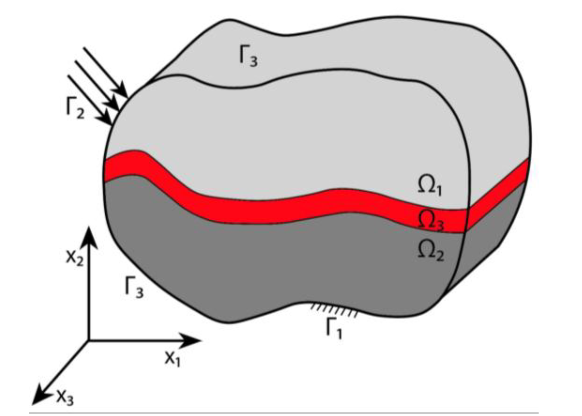
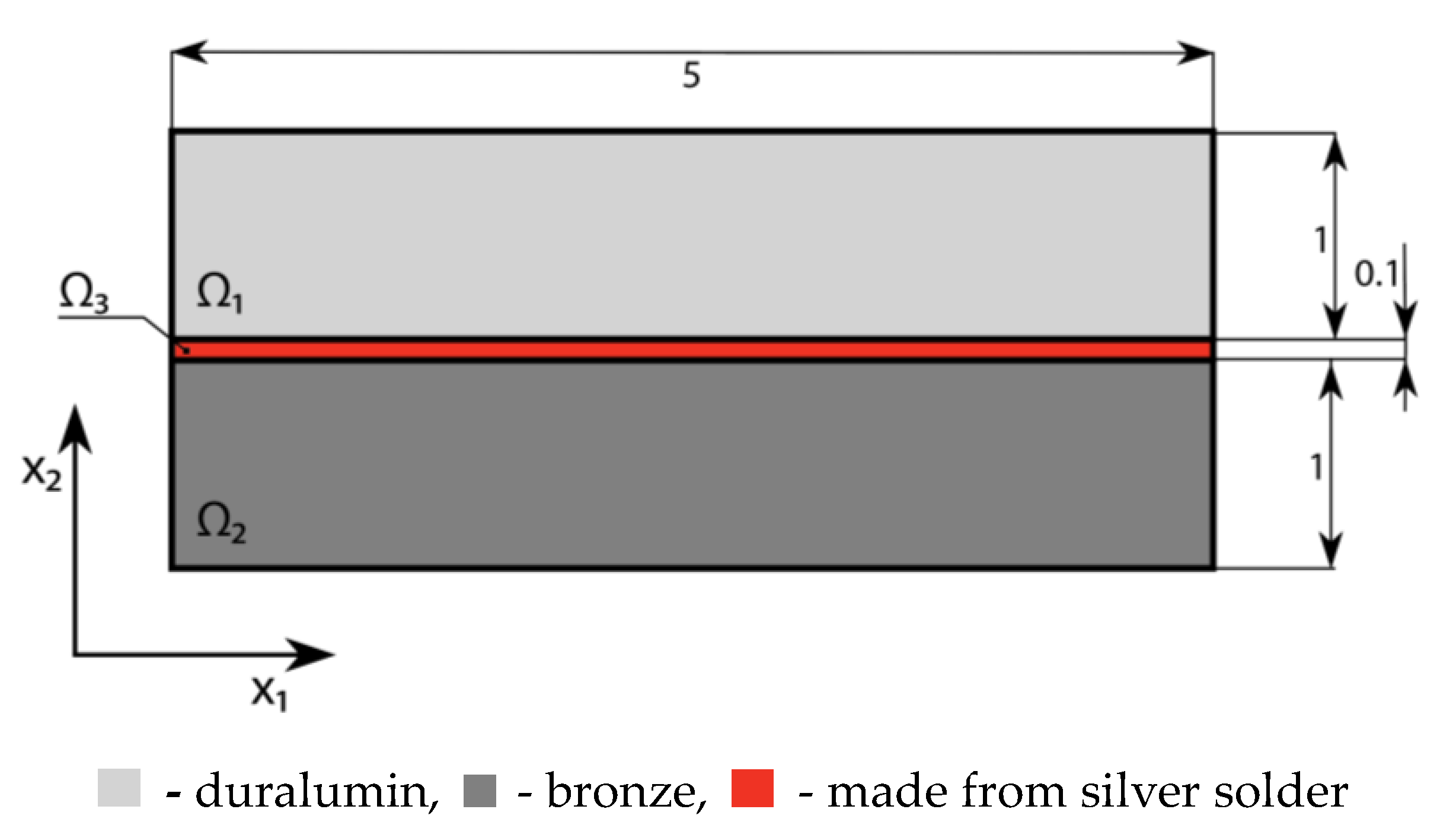
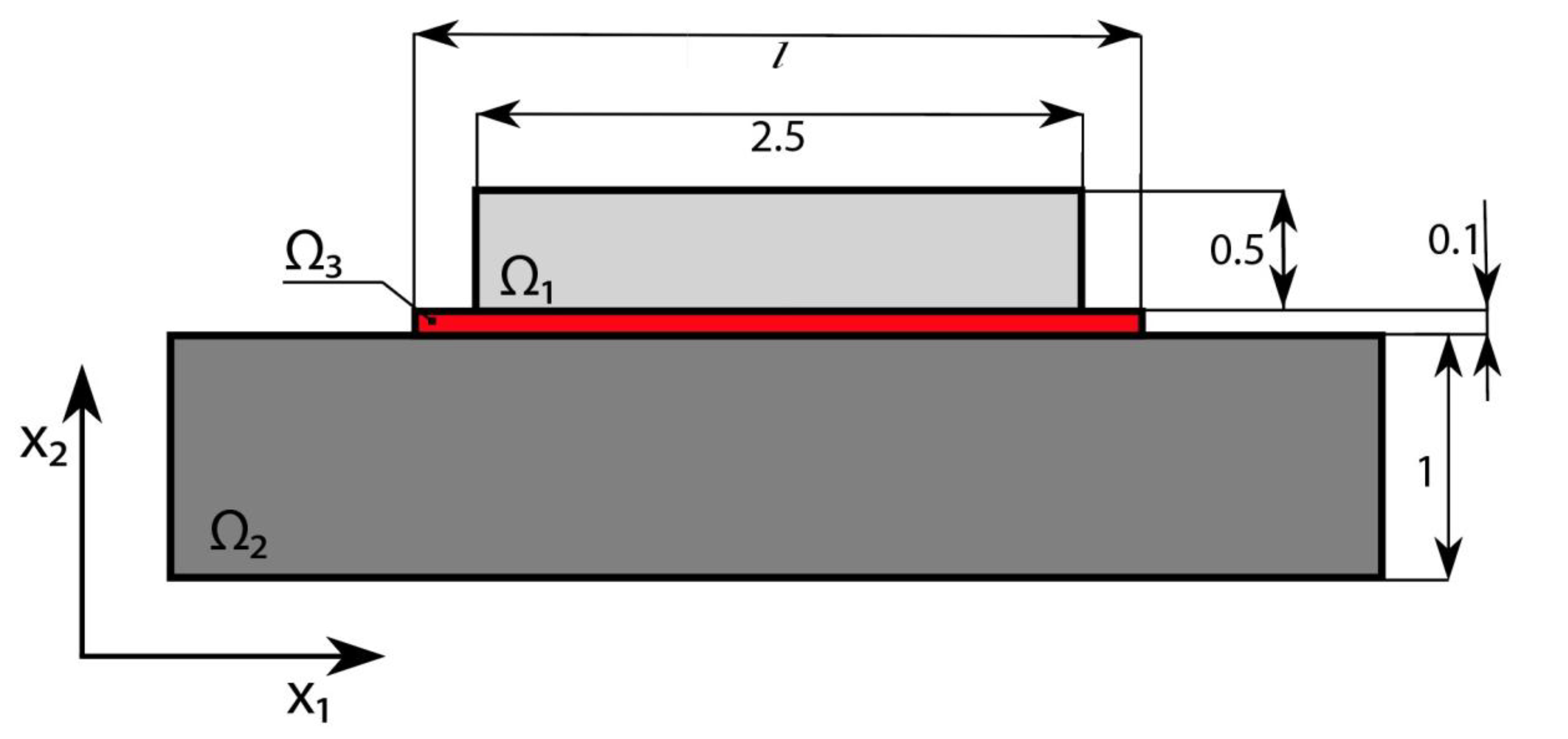
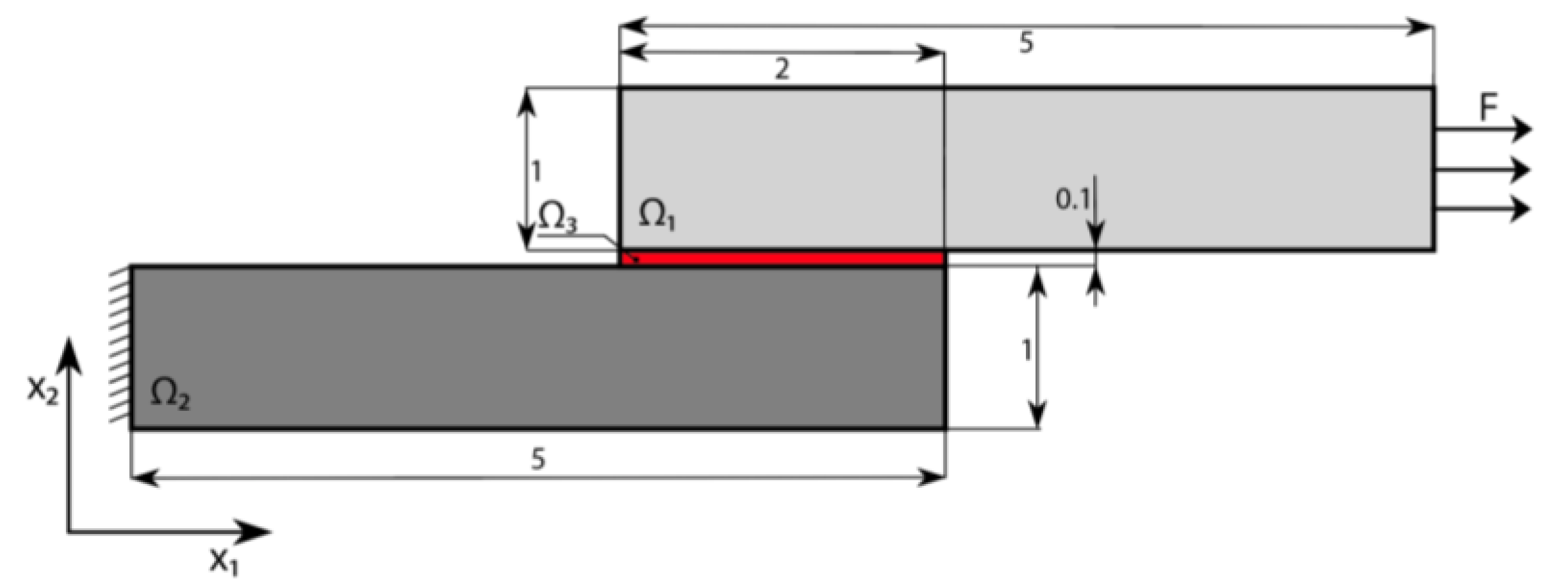
2. Problem Statement
3. Formulation of Topological Optimization Problem
4. Numerical Results of the Topological Optimization of Micro-Electronic Packages under Thermal Load
4.1. Case Study 1
4.2. Case Study 2
5. Topological Optimization of Non-Symmetric Packages under Thermal and Mechanical Loads: Numerical Results
6. Concluding Remarks
- A novel topological optimization methodology of structural soldered joints is developed.
- The proposed methodology yielded stresses decrease for an optimal structure.
- The main advantage of using topological optimization is that when designing structural elements, you do not need to know their geometry in advance.
- The numerical implementation of the developed methodology for strain calculations is performed by the finite element method using the method of moving asymptotes.
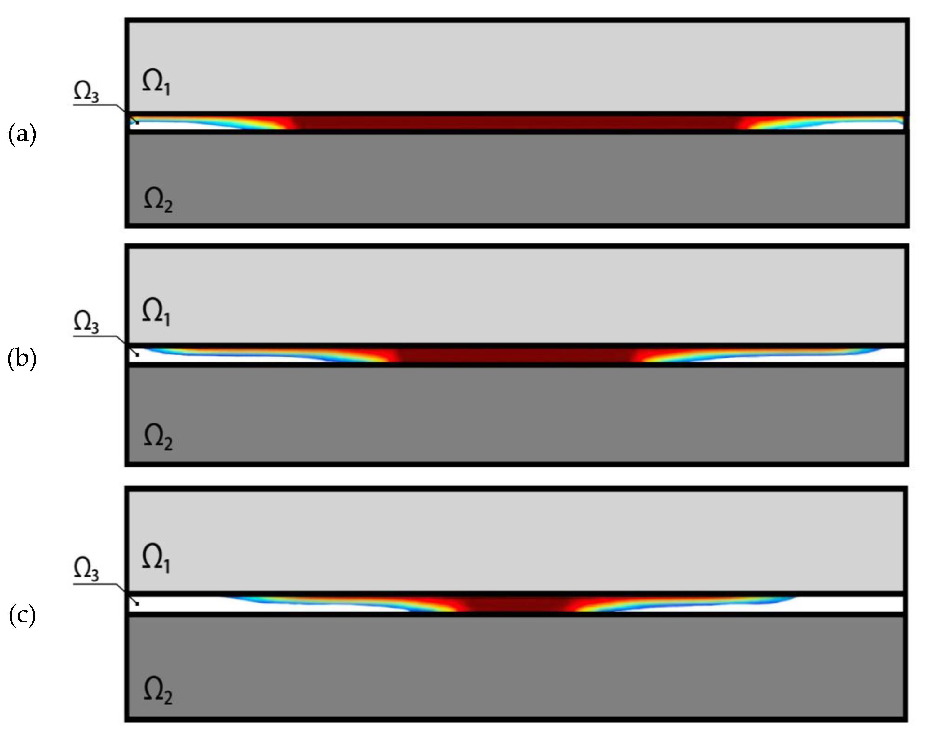
- In all cases, the constructed optimized structures demonstrate a significant decrease in the stress peaks in the solder layer at a smooth distribution of stresses along it, compared with a uniform solder layer.
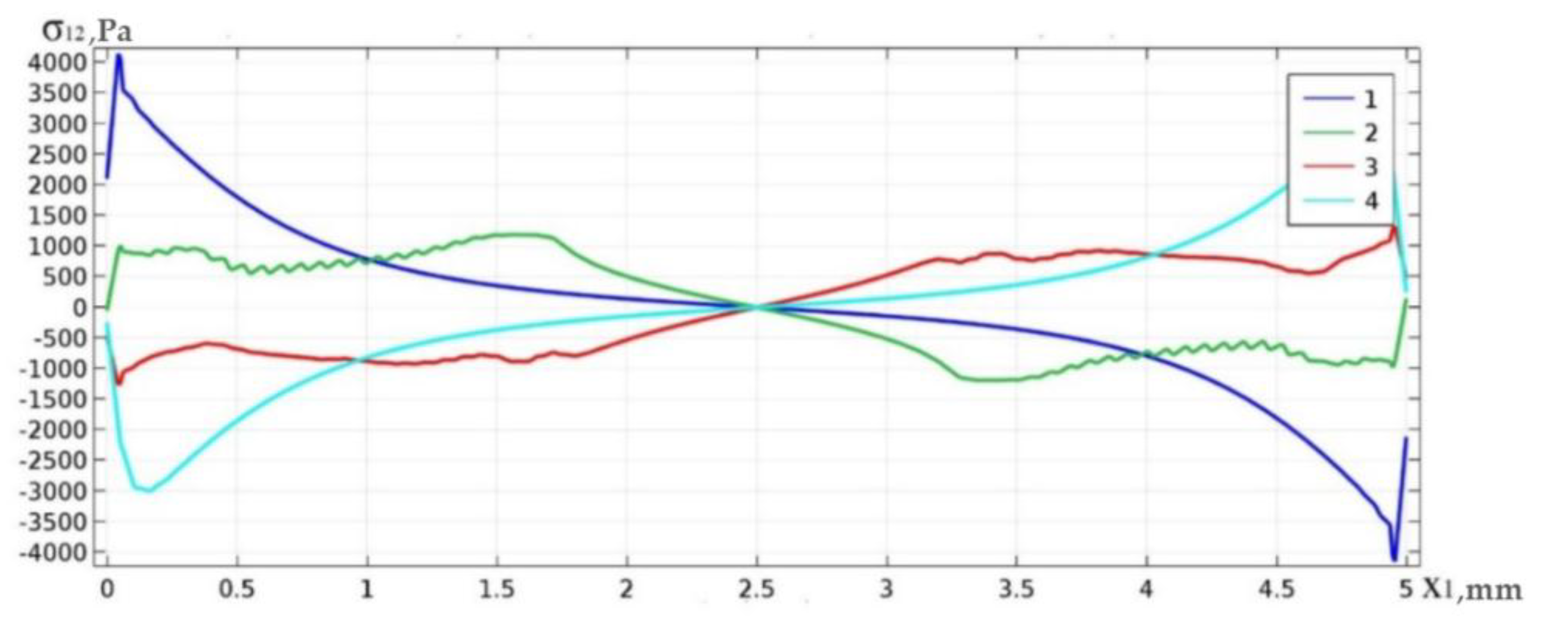
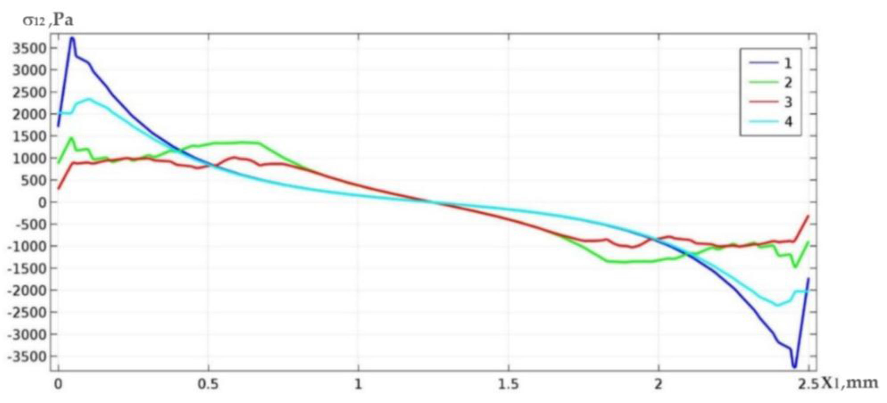
- The reliability is confirmed by the coincidence of numerical solutions obtained on the basis of the developed methodology for topological optimization with experimental data [6,7,8]. Peak stresses occur in small areas of the solder layer located near the connection ends; this coincides with the experimental results not reported here.
- The developed methodology based on topological optimization can be used in the design of macro and micro structures.
Author Contributions
Funding
Conflicts of Interest
References
- Hart-Smith, L.J. Design Methodology for Bonded-Bolted Composite Joints; Technical Report, AFWAL-TR-81-3154; Douglas Aircraft Company: Long Beach, CA, USA, 1982. [Google Scholar]
- Kelly, G. Quasi-static strength and fatigue life of hybrid (bonded/bolted) composite single-lap joints. Compos. Struct. 2006, 72, 119–129. [Google Scholar] [CrossRef]
- Da Silva, L.F.M.; Öschner, A.; Adams, R.D. Handbook of Adhesion Technology, 2nd ed; Springer: Heidelberg, Germany, 2018. [Google Scholar]
- Cattaneo, G.; Wagnild, G.; Marshall, G.; Watanabe, L. Comparison of tensile strength of solder joints by infrared and conventional torch technique. J. Prosthet. Dent. 1992, 68, 33–37. [Google Scholar] [CrossRef]
- Cheng, A.C.; Chai, J.Y.; Gilbert, J.; Jameson, L.M. Mechanical properties of metal connectors soldered by gas torch versus an infrared technique. J. Prosthodont. 1993, 2, 103–109. [Google Scholar] [CrossRef] [PubMed]
- Adams, R.D.; Comyn, J.; Wake, W.C. Structural Adhesive Joints in Engineering; Springer: Berlin, Germany, 1997. [Google Scholar]
- Dixon, D.G. Aerospace applications of adhesives. In Handbook of Adhesion; Packham, D.E., Ed.; John Wiley & Sons: Hoboken, NJ, USA, 2005. [Google Scholar]
- Watson, C. Engineering design with adhesives. In Handbook of Adhesion; Packham, D.E., Ed.; John Wiley & Sons: Hoboken, NJ, USA, 2005. [Google Scholar]
- Novotny, M.; Szendiuch, I. Lead-free solder joint quality investigation. Acta Electrotech. Infor. 2006, 6, 9708243. [Google Scholar]
- Lee, Y.; Basaran, C. A Creep Model for Solder Alloys. J. Electron. Packag. 2011, 133, 44501. [Google Scholar] [CrossRef]
- Samavatian, V.; Imaneini, H.; Avenas, Y. An efficient online time-temperature-dependent creep-fatigue rain flow counting. Int. J. Fat. 2018, 116, 284–292. [Google Scholar] [CrossRef]
- Breto, R.; Chiminelli, A.; Duvivier, E.; Lizaranzu, M.; Jimenez, M.A. Functionally Graded Bond-Lines for Metal/Composite Joints. In Proceedings of the ECCM16—16th European Conference on Composite Materials, Seville, Spain, 26 June 2014. [Google Scholar]
- Groth, H.L.; Nordlund, P. Shape optimization of bonded joints. Int. J. Adhes. Adhes. 1991, 11, 204–212. [Google Scholar] [CrossRef]
- Hildebrand, M. Non-linear analysis and optimization of adhesively bonded single lap joints between fibre-reinforced plastics and metals. Int. J. Adhes. Adhes. 1994, 14, 261–267. [Google Scholar] [CrossRef]
- Rispler, A.R.; Tong, L.; Steven, G.P.; Winsom, M.R. Shape optimisation of adhesive fillets. Int. J. Adhes. Adhes. 2000, 20, 221–231. [Google Scholar] [CrossRef]
- Taib, A.A.; Boukhili, R.; Achiou, S.; Gordon, S.; Boukehili, H. Bonded joints with composite adherends. Part I. Effect of specimen configuration, adhesive thickness, spew fillet and adherend stiffness on fracture. Int. J. Adhes. Adhes. 2006, 26, 226–236. [Google Scholar] [CrossRef]
- Lucas, F.M.; Da Silva, L.F.M.; Adams, R.D. Joint strength predictions for adhesive joints to be used over a wide temperature range. Int. J. Adhes. Adhes. 2007, 27, 362–379. [Google Scholar]
- Haghani, R.; Al-Emrani, M.; Kliger, R. Effects of Geometrical Modifications on Behavior of Adhesive Joints Used to Bond CFRP Laminates to Steel Members—Experimental Investigation; Chalmers Universityof Technology: Göteborg, Sweden, 2009. [Google Scholar]
- Lang, T.P.; Mallick, P.K. Effect of spew geometry on stresses in single lap adhesive joints. Int. J. Adhes. Adhes. 1998, 8, 167–177. [Google Scholar] [CrossRef]
- Belingardi, G.; Goglio, L.; Tarditi, A. Investigating the effect of spew and chamfer size on the stresses in metal/plastics adhesive joints. Int. J. Adhes. Adhes. 2002, 22, 273–282. [Google Scholar] [CrossRef]
- Frostig, Y.; Thomsen, O.T.; Mortensen, F. Analysis of adhesive-bonded joints, square-end and spew-fillet high-order theory approach. J. Eng. Mech.-ASCE 1999, 125, 1298–1307. [Google Scholar] [CrossRef]
- Akpinar, S.; Doru, M.O.; Ozel, A.; Aydin, M.D.; Jahanpasand, H.G. The effect of the spew fillet on an adhesively bonded single-lap joint subjected to bending moment. Compos. Part B Eng. 2013, 55, 55–64. [Google Scholar] [CrossRef]
- Zhao, X.; Adams, R.D.; Da Silva, L.F.M. Single lap joints with rounded adherend corners: Experimental results and strength prediction. J. Adhes. Sci. Tech. 2011, 25, 837–856. [Google Scholar]
- Zhao, X.; Adams, R.D.; Da Silva, L.F.M. Single lap joints with rounded adherend corners: Stress and strain analysis. J. Adhes. Sci. Tech. 2011, 25, 819–836. [Google Scholar]
- Matveenko, V.P.; Sevodina, N.V.; Fedorov, A.Y. Optimization of geometry of elastic bodies in the vicinity of singular points on the example of an adhesive lap joint. J. Appl. Mech. Tech. Phys. 2013, 54, 841–846. [Google Scholar] [CrossRef]
- Sancaktar, E.; Simmons, S.J. Optimization of adhesively-bonded single lap joints by adherend notching. J. Adhes. Sci. Tech. 2000, 14, 1363–1404. [Google Scholar] [CrossRef]
- Kaye, R.H.; Heller, M. Through-thickness shape optimisation of bonded repairs and lap-joints. Int. J. Adh. Adh. 2002, 22, 7–21. [Google Scholar] [CrossRef]
- Ejaz, H.; Mubashar, A.; Ashcroft, I.A.; Uddin, E.; Khan, M. Topology optimisation of adhesive joints using non-parametric methods. Int. J. Adh. Adh. 2018, 81, 1–10. [Google Scholar] [CrossRef]
- Chen, R.; Tseng, S.; Wan, C. Effects of solder joint structure and shape on thermal reliability of plastic ball grid array package. Int. J. Adv. Manuf. Technol. 2006, 27, 677–687. [Google Scholar] [CrossRef]
- Tian, Y.; Wang, C. Shape prediction and reliability design of BGA solder joint. Key Eng. Mater. 2005, 353–358, 2944–2947. [Google Scholar]
- Liu, X.; Lu, G. Effects of solder joint shape and height on thermal fatigue lifetime. IEEE Transact. Compon. Packag. Technol. 2003, 26, 455–465. [Google Scholar]
- Oterkus, E.; Barut, A.; Madenci, E.; Smeltzer, S.S.; Ambur, D.R. Nonlinear analysis of bonded composite joints. In Proceedings of the 45th AIAA/ASME/ASCE/AHS/ASC Structures, Structural Dynamics, and Materials Conference, Palm Springs, CA, USA, 19–22 April 2004. [Google Scholar]
- Hart-Smith, L.J. Adhesive-Bonded Scarf and Stepped-Lap Joints; Technical Report, NASA, CR112237; Douglas Aircraft Company: Long Beach, CA, USA, 1973. [Google Scholar]
- Boss, J.N.; Ganesh, V.K.; Lim, C.T. Modulus grading versus geometrical grading of composite adherends in single-lap bonded joints. Compos. Struct. 2003, 62, 113–121. [Google Scholar] [CrossRef]
- Kumar, S. Analysis of tubular adhesive joints with a functionally modulus graded bondline subjected to axial loads. Int. J. Adh. Adh. 2009, 29, 785–795. [Google Scholar] [CrossRef]
- Stapleton, S.E.; Waas, A.M.; Arnold, S.M. Functionally graded adhesives for composite joints. Int. J. Adh. Adh. 2012, 35, 36–49. [Google Scholar] [CrossRef] [Green Version]
- Spaggiari, A.; Dragoni, E. Regularization of torsional stresses in tubular lap bonded joints by means of functionally graded adhesives. Int. J. Adh. Adh. 2014, 53, 23–28. [Google Scholar] [CrossRef]
- Da Silva, L.F.M.; Lopes, M.J.C.Q. Joint strength optimization by the mixed adhesive technique. Int. J. Adh. Adh. 2009, 29, 509–514. [Google Scholar] [CrossRef]
- Pires, I.; Quintino, L.; Durodola, J.F.; Beevers, A. Performance of bi-adhesive bonded aluminium lap joints. Int. J. Adh. Adh. 2003, 23, 215–223. [Google Scholar] [CrossRef]
- Nimje, S.V.; Panigrahi, S.K. Numerical simulation for stress and failure of functionally graded adhesively bonded tee joint of laminated FRP composite plates. Int. J. Adh. Adh. 2014, 48, 139–149. [Google Scholar] [CrossRef]
- Das Neves, P.J.C.; Da Silva, L.F.M.; Adams, R.D. Analysis of mixed adhesive bonded joints part I: Theoretical formulation. J. Adh. Sci. Tech. 2009, 23, 1–34. [Google Scholar] [CrossRef]
- Das Neves, P.J.C.; Da Silva, L.F.M.; Adams, R.D. Analysis of mixed adhesive bonded joints part II: Parametric study. J. Adh. Sci. Tech. 2009, 61, 35–61. [Google Scholar] [CrossRef]
- Carbas, R.J.C.; Da Silva, L.F.M.; Madureira, M.L.; Critchlow, G.W. Modelling of functionally graded adhesive joints. J. Adh. 2014, 90, 698–716. [Google Scholar] [CrossRef]
- Da Silva, L.F.M.; Adams, R.D. Adhesive joints at high and low temperatures using similar and dissimilar adherends and dual adhesives. Int. J. Adh. Adh. 2007, 27, 216–226. [Google Scholar] [CrossRef]
- París, P.; Navarrina, F.; Colominas, I.; Casteleiro, M. Topology optimization of continuum structures with local and global stress constraints. Struct. Multidiscipl. Optimiz. 2009, 39, 419–437. [Google Scholar] [CrossRef]
- Qiu, G.Y.; Li, X.S. A note on the derivation of global stress constraints. Struct. Multidiscipl. Optimiz. 2010, 40, 625–628. [Google Scholar] [CrossRef]
- Stolpe, M.; Svanberg, K. An alternative interpolation scheme for minimum compliance topology optimization. Struct. Multidiscipl. Optimiz. 2001, 22, 116–124. [Google Scholar] [CrossRef]
- Le, C.; Norato, J.; Bruns, T.E.; Ha, C.; Tortorelli, D.A. Stress-based topology optimization for continua. Struct. Multidiscipl. Optimiz. 2010, 41, 605–620. [Google Scholar] [CrossRef]
- Herrick, R.W. Failure analysis and reliability of optoelectronic devices. In Microelectronics Failure Analysis; Ross, R.J., Ed.; ASM International: Material Park, OH, USA, 2011; pp. 78–98. [Google Scholar]
- París, J.; Navarrina, F.; Colominas, I.; Casteleiro, M. Global versus local statement of stress constraints in topology optimization. In Computer Aided Optimum Design of Structures; Alves, M., da Costa Mattos, H., Eds.; WIT Press: Southampton, UK, 2007; pp. 13–23. [Google Scholar]
- Svanberg, K. The method of moving asymptotes—A new method for structural optimization. Int. J. Num. Meth. Eng. 1987, 24, 359–373. [Google Scholar] [CrossRef]
- Awrejcewicz, J.; Pavlov, S.P.; Bodyagina, K.S.; Zhigalov, M.V.; Krysko, V.A. Design of composite structures with extremal elastic properties in the presence of technological constraints. Compos. Struct. 2017, 174, 19–25. [Google Scholar] [CrossRef]
- Krysko, A.V.; Awrejcewicz, J.; Pavlov, S.P.; Bodyagina, K.S.; Zhigalov, M.V.; Krysko, V.A. Non-linear dynamics of size-dependent Euler-Bernoulli beams with topologically optimized microstructure and subjected to temperature field. Int. J. Non-Lin. Mech. 2018, 104, 75–86. [Google Scholar] [CrossRef]
- Krysko, A.V.; Awrejcewicz, J.; Pavlov, S.P.; Bodyagina, K.S.; Krysko, V.A. Topological optimization of thermoelastic composites with maximized stiffness and heat transfer. Compos. Part B 2019, 158, 319–327. [Google Scholar] [CrossRef]


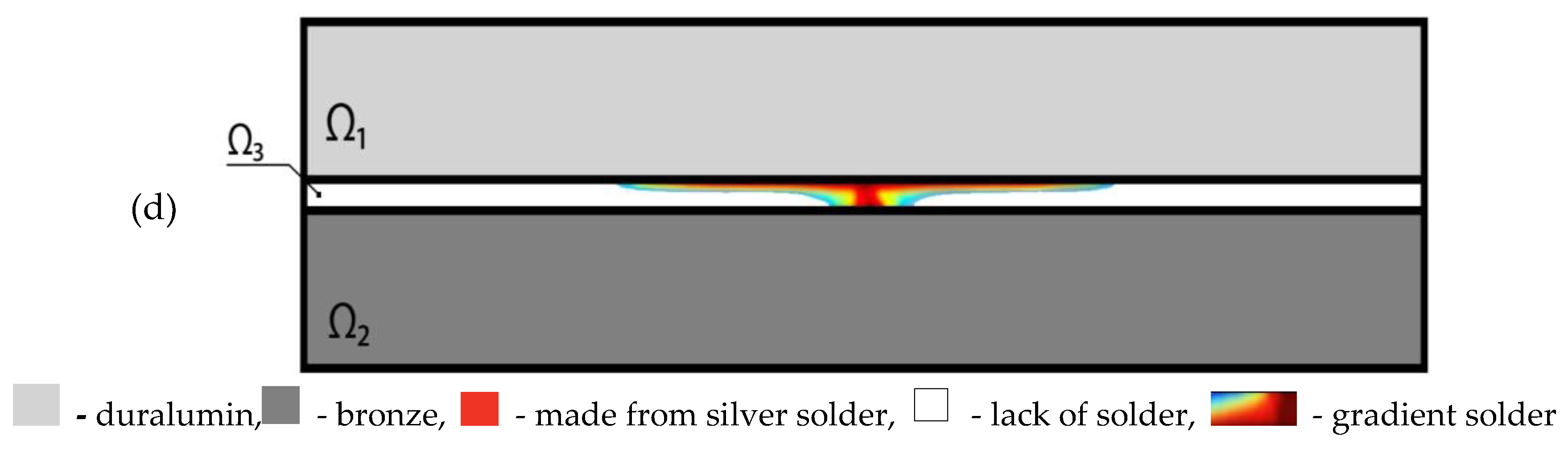
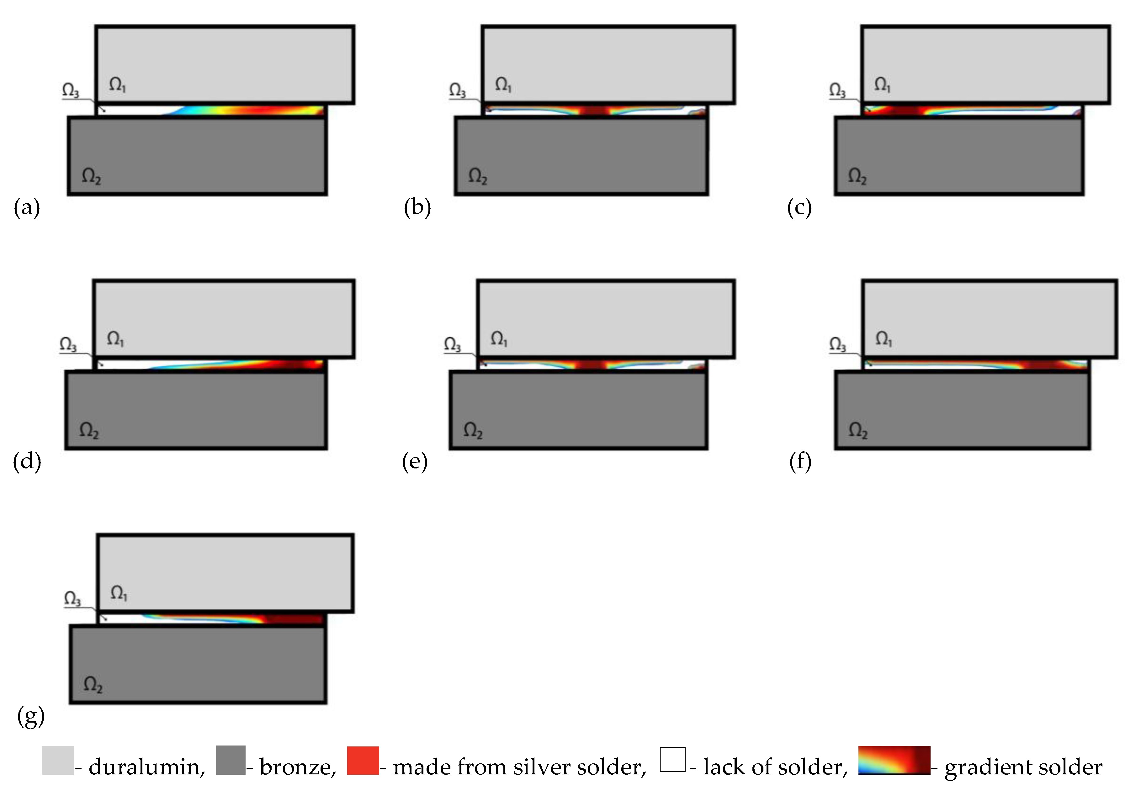
| γ | Topology of the Optimal Solder Structure | [GPa] | Δ [%] |
|---|---|---|---|
| 1 | Original construction | 1755.34 | 0.0 |
| 0.8 | Figure 4a | 894.74 | 60.0 |
| 0.6 | Figure 4b | 820.41 | 70.0 |
| 0.4 | Figure 4c | 700.14 | 75.0 |
| 0.2 | Figure 4d | 410.52 | 87.5 |
| l | Topology of Optimal Solder Structure | γ | [GPa] | Δ [%] |
|---|---|---|---|---|
| 4 | Original construction | 1 | 603.95 | 0.0 |
| Figure 6a | 0.75 | 564.93 | 60.0 | |
| 3 | Original construction | 1 | 804,41 | 0.0 |
| Figure 6b | 0.75 | 748.16 | 60.0 | |
| 2.5 | Original construction | 1 | 953.92 | 0.0 |
| Figure 6c | 0.75 | 876.61 | 61.0 |
| Topology of Optimal Solder Structure | mes(Ω3) | γ | [GPa] | Δ [%] |
|---|---|---|---|---|
| Figure 8a | 0.4 | 1 | 771.65 | 0.0 |
| 0.75 | 656.80 | 50.0 | ||
| Figure 8b | 0.4 | 1 | 809.65 | 0.0 |
| 0.75 | 739.75 | 60.0 | ||
| Figure 8c | 0.4 | 1 | 603.98 | 0.0 |
| 0.75 | 564.92 | 60.0 |
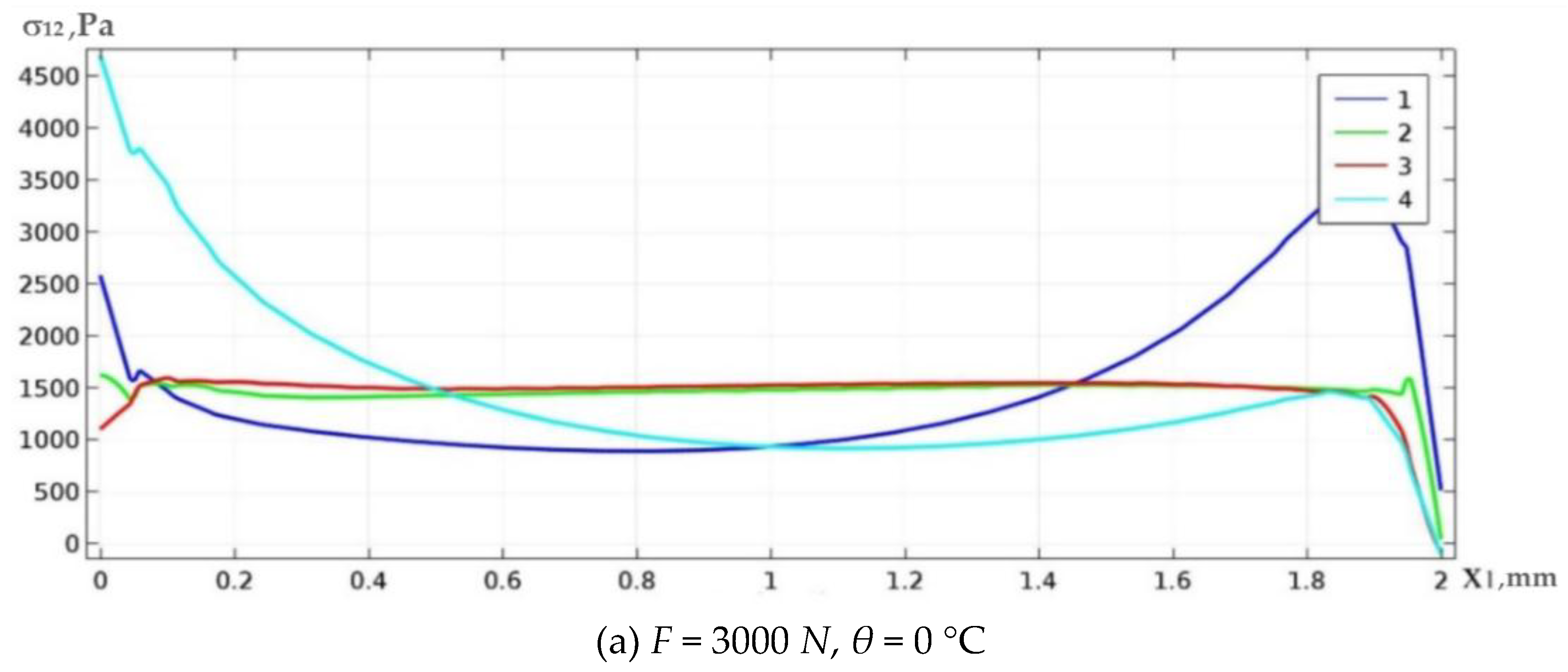
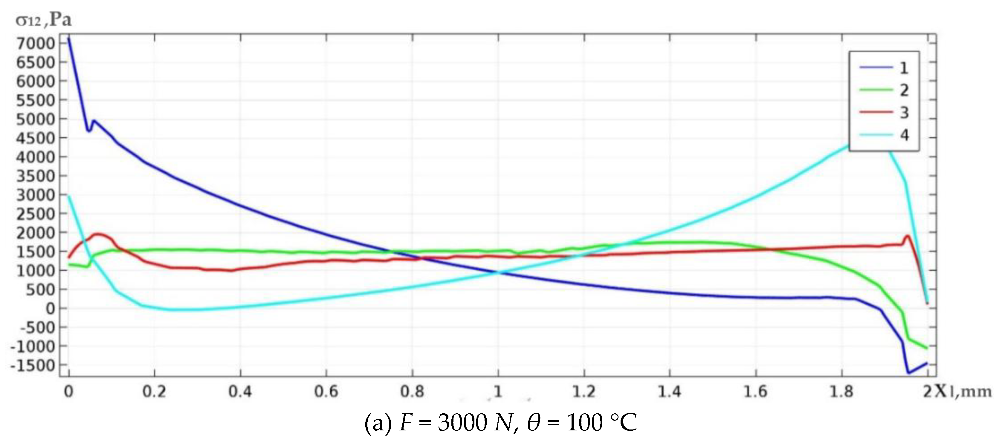
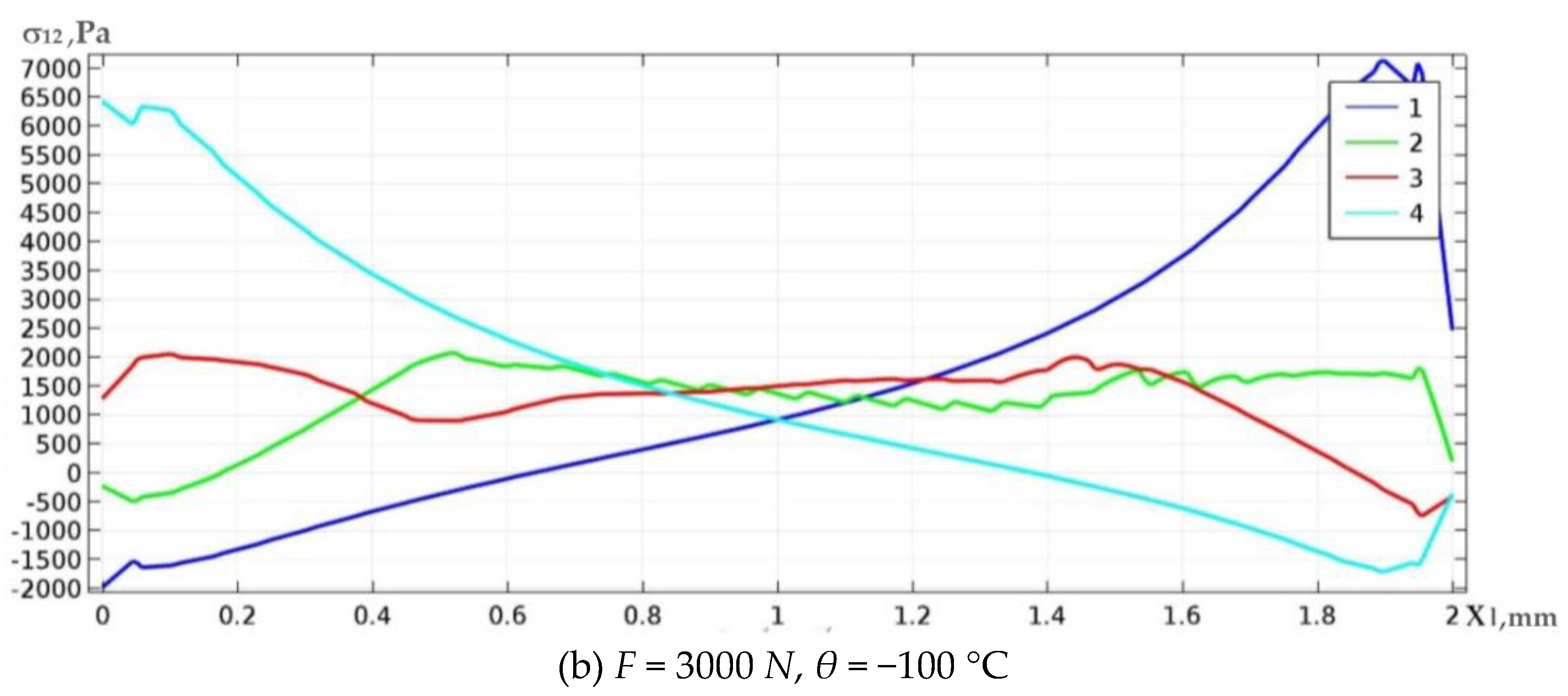
| F [N] | Topology of Optimal Solder Structure Shown in Figures | γ | [GPa] | Δ [%] | |
|---|---|---|---|---|---|
| 3000 | Original construction | 1 | 1501.15 | 0.0 | |
| Figure 10a | 0.5 | 1501.00 | 78 | ||
| 100 | 0 | Original construction | 1 | 1510.10 | 0.0 |
| Figure 10b | 0.5 | 620.00 | 72 | ||
| 1000 | Original construction | 1 | 1400.90 | 0.0 | |
| Figure 10c | 0.5 | 698.90 | 77.3 | ||
| 3000 | Original construction | 1 | 1524.95 | 0.0 | |
| Figure 10d | 0.5 | 1508.7 | 71.5 | ||
| −100 | 0 | Original construction | 1 | 1510.10 | 0.0 |
| Figure 10e | 0.5 | 620.00 | 72 | ||
| 1000 | Original construction | 1 | 1661.95 | 0.0 | |
| Figure 10f | 0.5 | 760.55 | 75 | ||
| 3000 | Original construction | 1 | 2080.00 | 0.0 | |
| Figure 10g | 0.5 | 1562.90 | 69 |
© 2020 by the authors. Licensee MDPI, Basel, Switzerland. This article is an open access article distributed under the terms and conditions of the Creative Commons Attribution (CC BY) license (http://creativecommons.org/licenses/by/4.0/).
Share and Cite
Awrejcewicz, J.; Pavlov, S.P.; Krysko, A.V.; Zhigalov, M.V.; Bodyagina, K.S.; Krysko, V.A. Decreasing Shear Stresses of the Solder Joints for Mechanical and Thermal Loads by Topological Optimization. Materials 2020, 13, 1862. https://doi.org/10.3390/ma13081862
Awrejcewicz J, Pavlov SP, Krysko AV, Zhigalov MV, Bodyagina KS, Krysko VA. Decreasing Shear Stresses of the Solder Joints for Mechanical and Thermal Loads by Topological Optimization. Materials. 2020; 13(8):1862. https://doi.org/10.3390/ma13081862
Chicago/Turabian StyleAwrejcewicz, Jan, Sergey P. Pavlov, Anton V. Krysko, Maxim V. Zhigalov, Kseniya S. Bodyagina, and Vadim A. Krysko. 2020. "Decreasing Shear Stresses of the Solder Joints for Mechanical and Thermal Loads by Topological Optimization" Materials 13, no. 8: 1862. https://doi.org/10.3390/ma13081862