Structure and Photoluminescence Properties of Thermally Synthesized V2O5 and Al-Doped V2O5 Nanostructures

1
Department of Materials Science and Engineering, National Chung Hsing University, Taichung 40227, Taiwan
2
Department of Chemical Engineering and Materials Science, Chinese Culture University, Taipei 11114, Taiwan
*
Authors to whom correspondence should be addressed.
Materials 2021, 14(2), 359; https://doi.org/10.3390/ma14020359
Submission received: 11 December 2020
/
Revised: 5 January 2021
/
Accepted: 11 January 2021
/
Published: 13 January 2021
(This article belongs to the Collection Luminescent Materials)
Abstract
:Al-free and Al-doped V2O5 nanostructures were synthesized by a thermal-chemical vapor deposition (CVD) process on Si(100) at 850 °C under 1.2 × 10⁻¹ Torr via a vapor-solid (V-S) mechanism. X-ray diffraction (XRD), Raman, and high-resolution transmission electron microscopy (HRTEM) confirmed a typical orthorhombic V2O5 with the growth direction along [110]-direction of both nanostructures. Metallic Al, rather than Al3+-ion, was detected by X-ray photoelectron spectroscopy (XPS), affected the V2O5 crystallinity. The photoluminescence intensity of V2O5 nanostructure at 1.77 and 1.94 eV decreased with the increasing Al-dopant by about 61.6% and 59.9%, attributing to the metallic Al intercalated between the V2O5-layers and/or filled in the oxygen vacancies, which behaved as electron sinks. Thus the Al-doped V2O5 nanostructure shows the potential applications in smart windows and the electrodic material in a Li-ion battery.
1. Introduction
Vanadium is a multi-valent element with oxidation states of V2+, V3+, V4+, and V5+, and therefore has several phase-states, including vanadium monoxide (VO), vanadium sesquioxide (V2O3), vanadium dioxide (VO2), and vanadium pentoxide (V2O5) [1,2]. Vanadium pentoxide (V2O5) is the most stable phase; it has an orthorhombic structure and layered VO5 structures of square pyramids that share corners and edges [3,4]. The layered structure results in the V3d split-off conduction band so that V2O5 has direct and indirect band gaps at 2.3 and 1.9 eV [5]. Oxygen vacancies () are the most common defects in V2O5, and especially in the oxygen layer in the layered VO5 structure [6]. The conduction band that has split off and the -defects provide a flexible pathway for luminescence. Doping with elements and the formation of the core-shell nanostructures modify the photoluminescence properties [7,8]. Many works have reported upon methods of fabricating V2O5, which are: atomic layer chemical vapor deposition [9], the sol-gel process [10], thermal deposition [11], the hydrothermal process [12], and the thermal evaporation process [7,8]. The photoluminescence property of V2O5 can be modified by the different dopants, such as Er [13], Co [14], Nd [15,16], Gd [16]; Al [10], and Ga [7]. The above doped V2O5 materials possess potential applications in light emitters, photocatalysts, and cathodic materials for ionic batteries. Owing to the layered structures and tunable photoluminescence properties, V2O5 has many applications, including electrochromic devices [17], solar cells [18,19], catalysts [20], solid-state batteries [21], gas sensors [22], chemical species sensors [23], smart windows [4], etc. The dopants as mentioned above were not metallic powders. Instead, the nitrate [10,13,15], sulfate [14], and oxide powders [16] were the dopants, which implied that the metallic ions were easy to form during the synthesized process, resulting in the subsequent influence in photoluminescence. However, the zero-valent metallic ion can also show the influence in the photoluminescence property. Compared to previous literature [7,10,13,14,15,16], this work shows for the first time the metallic Al powders acting as dopants and doping V2O5 nanostructures. This implies that the zero-valent and/or tri-valent Al ions can be observed, and their influence in the photoluminescence property of the V2O5 nanostructures can be studied. Al-doped V2O5 shows potential applications including as photodiode [24], in electrocatalysis [25], thin-film batteries [26], and as cathodic materials for lithium ion batteries [10].
In this work, metallic Al powder was directly used as a source of metallic Al dopant. Both Al-free and Al-doped V2O5 nanostructures (NSs) were fabricated on Si(100) substrate using a thermal-chemical vapor deposition (CVD) process via a catalyst-free vapor-solid (V-S) mechanism at 850°C under 1.2 × 10⁻¹ Torr. In addition, Ar gas was introduced during the whole synthesized process to lower the oxygen partial pressure and to prevent the formation of the Al2O3 phase. The effects of Al doping on the crystal structures, binding energies, bonding vibration modes, and luminescence properties of V2O5 NSs are systematically analyzed based on the results of X-ray diffraction (XRD), high-resolution transmission electron microscopy (HRTEM), and Raman, and photoluminescence spectra.
2. Materials and Methods
2.1. Fabrication of Al-Free and Al-Doped V2O5 Nanostructures
Al-free V2O5 NSs were deposited on the Si (100) substrates by the catalyst-free V-S mechanism using the thermal-CVD process at 850 °C in a quartz tube furnace. A 0.3 g mass of high-purity V2O5 powder (Aldrich, Shanghai, China, 99.5%) was placed in an alumina crucible in the center of the quartz tube; about 10cm downstream of the crucible was placed the Si (100) substrate. The system pressure was pumped down to 4.0 × 10⁻² Torr and the temperature was increased to 850 °C at 25 °C/min in Ar 30 standard cubic centimeter per minute (sccm) V2O5 powder was evaporated at 850 °C for 1.5 h, and its vapor was mixed with Ar (30 sccm) and O2 (20 sccm) at 1.2 × 10⁻¹ Torr; V2O5 NSs were grown on Si(100) substrate and then cooled to room-temperature at 30 sccm Ar. The final products were denoted as AV0 NSs. Al-doped V2O5 NSs were synthesized in a similar manner. The starting materials were a mixture of 0.3 g powdered V2O5 with various amounts of powdered Al (Aldrich, 99.9%)—1.5 mg (0.5 wt.%), 3 mg (1 wt.%), and 4.5 mg (1.5 wt.%)—that were co-evaporated at 850 °C to yield AV05, AV10, and AV15, respectively.
Before analyzing processes, all samples were preserved in a glass desiccator under the pressure of 1 Torr. The samples of the AV nanostructures being covered on the Si(100) substrates were directly analyzed using XRD, X-ray photoelectron spectroscopy (XPS), field-emission scanning electron microscopy (FESEM), Raman, and photoluminescence (PL). The AV nanostructures were detached from the Si(100) substrate by ultrasonication in the ethanol solution, followed by the HRTEM observation.
2.2. Characterizations
The crystal structures of the AV NSs were determined using a mass absorption coefficient glancing incident X-ray diffractometer with Cu kα radiation source (λ = 0.154 nm, 40 kV, 30 A, Bruker D2 PHASER) in the recording range from 20 to 60° and high-resolution transmission electron microscope with the electron accelerating voltage of 200 kV (HRTEM, JEOL, JEM-3000F, Tokyo, Japan). The chemical binding energies were measured by X-ray photoelectron spectroscope using the Al kα radiation with the electron energy of 1486.6 eV (XPS, Perkin-Elmer model PHI1600 system, Waltham, MA, USA). The chemical bonding vibration modes were identified by Raman spectrometer (3D Nanometer Scale Raman PL microspectrometer, Tokyo Instruments, INC., Tokyo, Japan) with an excitation source of a semiconductor laser at the wavelength of 532 nm. Room-temperature PL spectra were recorded by a confocal Raman spectrometer (Alpha300, Witec, Ulm, Germany) with the source of semiconductor laser (λ = 532 nm, 0.5 mW).
3. Results
3.1. X-ray Photoelectron Spectroscopy (XPS) Analysis
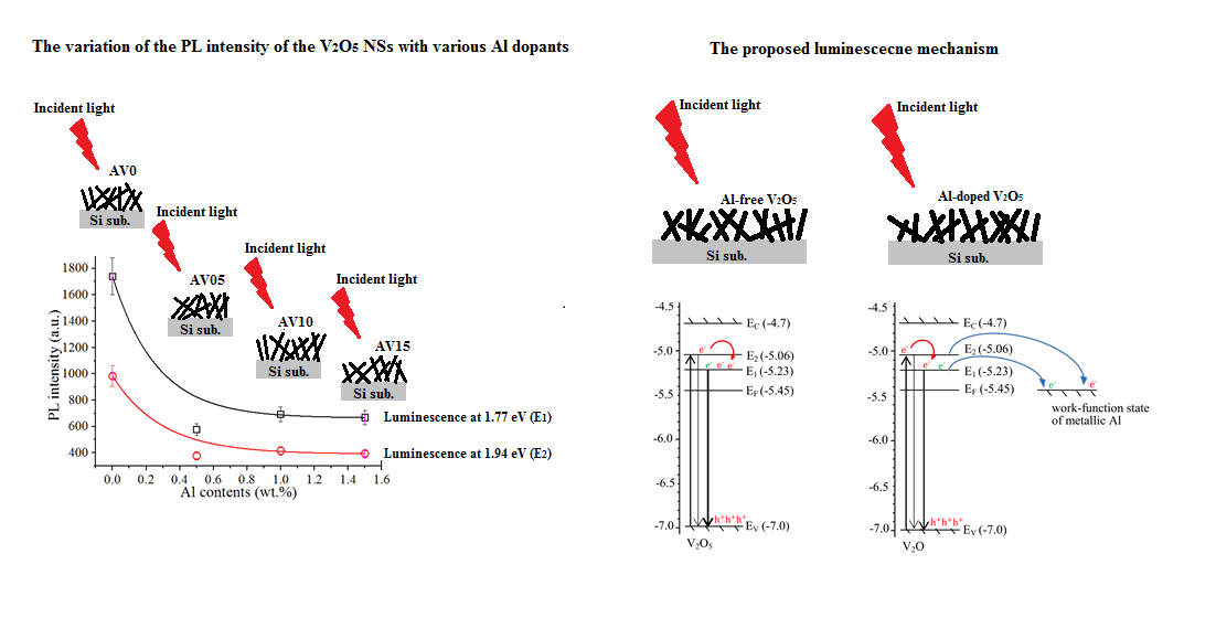
Figure 1a presents the XPS spectra of the V 2p and O 1s orbitals of AV0 and AV15 NSs. The peaks at 516.4 eV (V 2p3/2) and 523.7 eV (V 2p1/2) of the AV0 NSs with a splitting Δ-value of 7.3 eV are consistent with the characteristic of orthorhombic V2O5 structures [27]. The AV15 NSs show a similar splitting Δ-value (7.4 eV), indicating that the Al dopants do not affect the V2O5 orthorhombic structure. The O 1s peak at 529.3 eV is attributed to the oxygen ions (OL) associated with the V–O bonds in the V2O5 structures [28,29]; the peak at 530.7 eV (OC) is attributed to the chemisorbed oxygen on the surface of the NSs [7]. The energy difference between V 2p3/2 and OL is about 12.9 eV, indicating the formation of the V2O5 phase [29]. The values of V 2p and OL in the AV15 NSs (Figure 1a) are similar to those of the AV0 NSs. However, the binding energy of OC in AV15 NSs shifts upward to 532.2 eV relative to that of AV0 NSs (530.7 eV). The reduction potential of Al is as low as −0.677 V [30], indicating that Al more easily reacts with oxygen-containing species, such as oxygen and/or hydroxyl, and forms the amorphous phases of Al–O and/or Al–OH [31] at the surface of the NSs.
Therefore, the OC position in AV15 NSs ends up with a blue-shift. Figure 1b shows that the energies of the Al 2p orbitals in AV05, AV10, and AV15 NSs have the same binding energy of 72.12 eV [32], showing that the Al dopants behave as a metal rather than the ions in the V2O5 NSs. Table 1 presents the atomic percentage (at.%) of Al in the V2O5 NSs, indicating that the at.% of Al dopant increases with Al contents.
3.2. X-ray Diffraction (XRD) Patterns
The powder XRD analysis of both Al-free and Al-doped V2O5 NSs reveal the typical orthorhombic V2O5 structure (joint committee on powder diffraction standard (JCPDS) 77-2418) with the planes (001), (110), (400), (111), (002), and (600) at diffraction angles of 20.36, 26.16, 31.06, 33.01, 41.37, and 47.35°, correspondingly, as presented in Figure 2. No irrelevant phases, such as Al2O3 and metallic Al, were detected. The insets in Figure 2a reveal that the full width at half maximum (FWHM) of the V2O5 (001) plane varies with the Al content and show a deviation of ±2.9% of all the AV NSs, indicating that the Al dopants do not affect the V2O5 crystal structure.
Based on the Bragg law and the plane-spacing equation for an orthorhombic structure, , the lattice constants (a, b, and c), and the ratios c/a and c/b can be estimated; they are provided in Table 2. Both c/a and c/b ratios increase with the addition of Al dopant, as shown in Figure 2b. The V2O5 comprises packed layered [VO5]–[VO5] structures, facilitating the formation of between the layers [8,11]. The radius of the Al0 is 1.43 Å similar to the (1.4 Å). The interlayer spacing of the layered V2O5 structure is about 4.32 Å [33].
Therefore, the increase in c/a and c/b can be attributed to the filling by Al0 of the sites of and/or intercalating between the two layered VO5 structures in V2O5 NSs. The Al dopant slightly increases the lattice distance between the two [VO5]-layers in the a–c plane (inset in Figure 2b [34]) by approximately 0.1–0.2% when the Al content is ≤1 wt.% and a more significant increase of the lattice distance (by 1.2%) at an Al-dopant content of 1.5 wt.%. The lattice spacing in the a–b plane (inset in Figure 2b [34]) significantly increases with the incorporation of Al dopant. These results reveal that the c/b and c/a ratios increase with the incorporated Al dopants in the V2O5 NSs.
3.3. Field-Emission Scanning Electron Microscopy (FESEM) and High-Resolution Transmission Electron Microscopy (HRTEM) Analysis
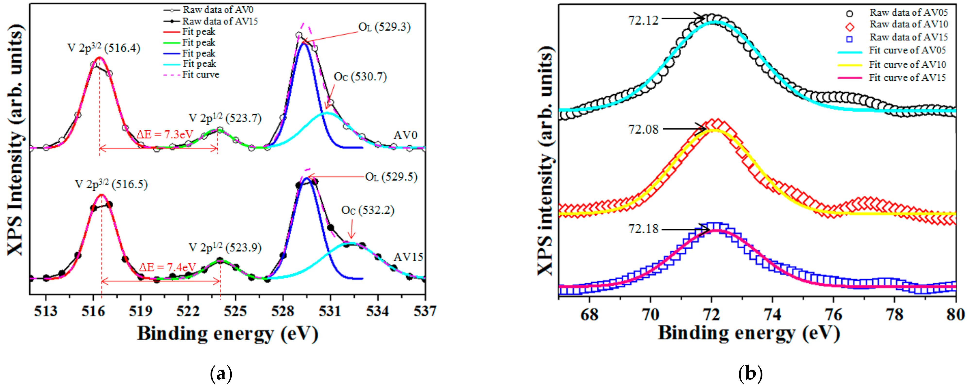
FESEM images of AV0 and AV10 NSs are shown in Figure 3a,b. Most of the nanostructures exhibit the nanowire-like shape. Their crystal structure and growth direction are estimated by the following HRTEM analysis and shown in Figure 3c,d. Inset 1 (Figure 3c) shows d-spacings of 5.7 and 3.6 Å, consistent with the planes V2O5 (100) and V2O5 (110); the angle between the (100) and (110) planes is 72°, consistent with the selective area diffraction (SAD) pattern in inset 2 (Figure 3c). The d-spacings of AV10 NSs, as shown in inset 3 (Figure 3d), are 4.2 and 3.4 Å, consistent with the planes V2O5 (001) and V2O5 (110) and the angle between (001) and (110) is 89.5°, consistent with the SAD pattern in inset 4 (Figure 3d). The theoretical angles between (110) and (200) and between (110) and (001) are 73° and 90°, respectively, which are estimated using the formula, , where is the angle between the (h1k1l1) plane and the (h2k2l2) plane; a (11.51 Å), b (3.559 Å), and c (4.371 Å) are the lattice constants of the orthorhombic V2O5 structure Based on the above discussion, the growth direction of the AV NSs can thus be confirmed as being in the [110]-direction.
3.4. Raman Spectra
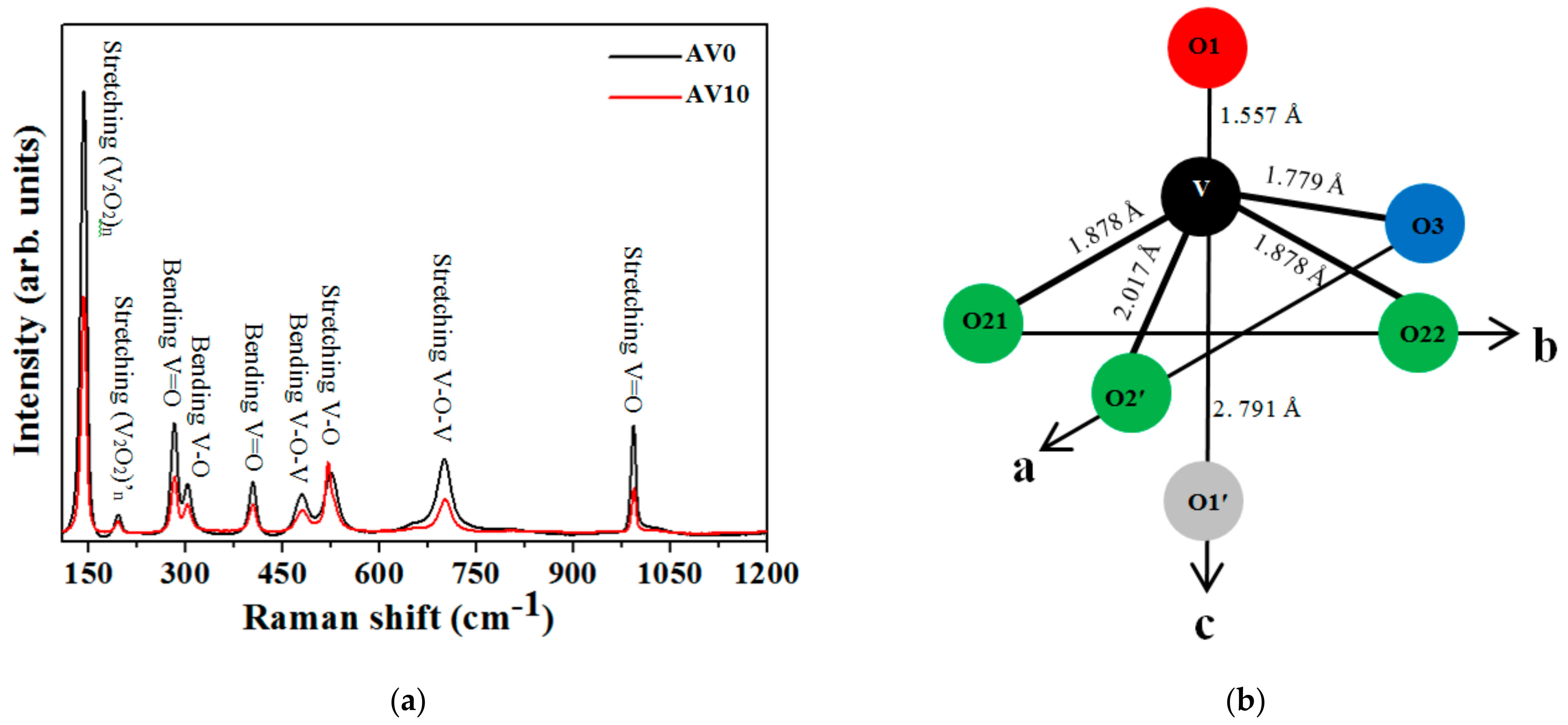
The V2O5 structure is orthorhombic and has a Pmnm symmetry; V2O5 has typical Raman active peaks of AV0 and AV10 NSs which fitted by Gaussian deconvolution are observed at around 141.71, 195.26, 282.04, 302.64, 403.51, 480.45, 524.80, 699.93, and 993.36 cm−1 [3,35,36,37], as shown Figure 4a and listed in Table 3. The crystal structure of V2O5 NSs is layered V2O5s that is packed along the c-axis of the unit cell, and each V2O5 layer comprises square pyramids of VO5 that share edges and corners, as shown in Figure 4b [8,38]. One vanadium atom is connected to six oxygen atoms with five bond lengths, which are of 1.557, 1.779, 1.878, 2.017, and 2.791 Å, as shown schematically in Figure 4b [38]. The V–O1 bond has the strongest binding energy but the shortest bonding length (1.557 Å) of all of the V–O bonds; the V–O1′ bond is a weak Van der Waals’ bond between layered-VO5 with a bonding length of 2.791 Å; along the b-axis, the V–O21 and V–O22 bonds have a length of 1.878 Å; along the a-axis, the V–O bonds are of two types:
- (1)
- The V–O2′1 bond has a length of 2.017 Å, and
- (2)
- The V–O3 bond has a length of 1.779 Å.
Figure 4.
(a) Raman spectra of the AV0 and AV10 NSs, and (b) schematic V2O5 molecular Scheme [38].
Figure 4.
(a) Raman spectra of the AV0 and AV10 NSs, and (b) schematic V2O5 molecular Scheme [38].


Table 3.
Characteristic Raman shifts of the nanostructures of AV0 and AV10 NSs.
| Raman Scattering Modes | AV0 NSs | AV10 NSs | Deviation of the Raman Shifts (%) | ||
|---|---|---|---|---|---|
| Raman Shifts (cm−1) | Intensity | Raman Shifts (cm−1) | Intensity | ||
| Stretching (V2O2)n | 141.71 | 84,745.82 | 141.93 | 45,097.12 | 0.071 |
| Stretching (V2O2)’n | 195.26 | 3371.40 | 194.45 | 1830.32 | 0.051 |
| Bending V=O | 282.04 | 20,894.35 | 282.14 | 10,431.08 | 0.017 |
| Bending V–O | 302.64 | 9033.58 | 302.47 | 5007.98 | 0.016 |
| Bending V=O | 403.51 | 9475.78 | 403.33 | 4967.71 | 0.025 |
| Bending V–O–V | 480.45 | 6944.95 | 481.35 | 3846.47 | 0.062 |
| Stretching V–O | 524.80 | 11,097.60 | 522.07 | 11,202.89 | 0.258 |
| Stretching V–O–V | 699.93 | 12,863.33 | 701.25 | 5757.458 | 0.099 |
| Stretching V=O | 993.36 | 20,228.08 | 994.02 | 8188.87 | 0.030 |
This orthorhombic V2O5 structure has two bonding vibrations. They are: (1) stretching mode: the terminal oxygen of the V=O bond is the unshared oxygen (O1) and yields a peak at 993.36 cm−1 [39,40]; the doubly coordinated oxygen in the V–O–V bond is a corner-sharing oxygen in one of the two adjacent pyramids yields a peak at 699.93 cm−1 [41]; the triply coordinated oxygen of the V–O bond is an edged-sharing oxygen in three adjacent pyramids yields a peak at 524.80 cm−1 [6,39]; and (2) bending mode: the bridging V–O–V bond at 480.45 cm−1 [39,41]; the terminal oxygen associated with the V=O bond yields a peak at 403.51 cm−1 [40]; the triply coordinated oxygen associated with the V–O bond yields a peak at 302.64 cm−1 [6]; the V=O terminal oxygen associated with the bond yields a peak at 282.04 cm−1; (V2O2)n and (V2O2)’n bonds yield peaks at 194.26 and 141.71 cm−1, respectively, corresponding to the chain translation and strongly associated with the layered structures [41]. Table 3 presents the Raman shifts of the AV0 and AV10 NSs. The deviations of the Raman shifts upon the addition of Al reveal a slight difference between AV0 and AV10 NSs, indicating that Al has no major effect on the V2O5 binding structures, which is consistent with the XPS results.
The intensity of the Raman peaks (as shown in Figure 4a and Table 3) clearly decreases upon the addition of Al dopant. Jung et al. [42] reported a decrease in the Raman intensity from V2O5 upon the insertion of Li into the LixV2O5 lattice owing to the formation of negative charge carriers by the reduction of V5+ to V4+ [43]; Park et al. determined that the decreasing Raman intensity is attributable to the extraction of Li from the LixCoO2 lattice because the oxidization state increases from Co3+ to Co4+, generating positive charge carriers [44,45]. Both of these cases are attributable to the metallization of the host materials, so decreases in Raman intensity arise from the reduction of the optical skin depth of the Raman excitation light [42]. In this work, metallic Al is doped into the V2O5 lattice, as revealed by XPS and XRD; the host materials, therefore, exhibit more metallic characters. Hence, the Raman intensity of the V2O5 NSs clearly decreases with the addition of Al (Figure 4a).
3.5. Photoluminescence (PL) Spectra
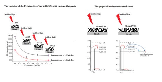
Figure 5a presents the PL spectra of the AV NSs, which reveal two prominent emissions at 1.77 (E1) and 1.94 eV (E2). V2O5 has split-off conduction bands owing to its layered structure, suggesting that it has several energy bands from the top of the O2p valance band to the split-off V3d conduction band [11]. The V2O5 crystal structure comprises from the [VO5]-[VO5] layers and oxygen vacancies () easily being formed between the layers [11]. Accordingly, the -related emission E1 occurs at 1.77 eV and E2 at 1.94 eV is attributed to the intrinsic emission band, which is split off from the V3d conduction band in the V2O5 NSs [6,46]. Figure 5b presents variations of the intensities of E1 and E2 with the Al content. Such variations in luminescence intensities decay exponentially as Al content increases. The intensity of E1 decreases by about 61.6% and that of E2 decreases by about 59.9% as the Al content increases from 0 to 1.5 wt.%.
Table 4 shows the influence in the photoluminescence intensity of the V2O5 by different dopants, including metallic Al, metallic Ga [7], aluminum nitrate nonahydrate (Al(NO3)3·9H2O) [10], erbium nitrate pentahydrate (Er(NO3)3·5H2O) [13], cobalt sulfate heptahydrate (CoSO4·7H2O) [14], gadolinium oxide (Gd2O3) [16], neodymium oxide (Nd2O3) [16], aluminum nitrate (Al(NO3)3) [24], and aluminium oxide (Al2O3) [26]. Besides the Ga dopants, the PL intensities of V2O5 decrease with the zero-valent Al the same as the results of the tri-valent elements.
3.6. Proposed Luminescence Mechanism
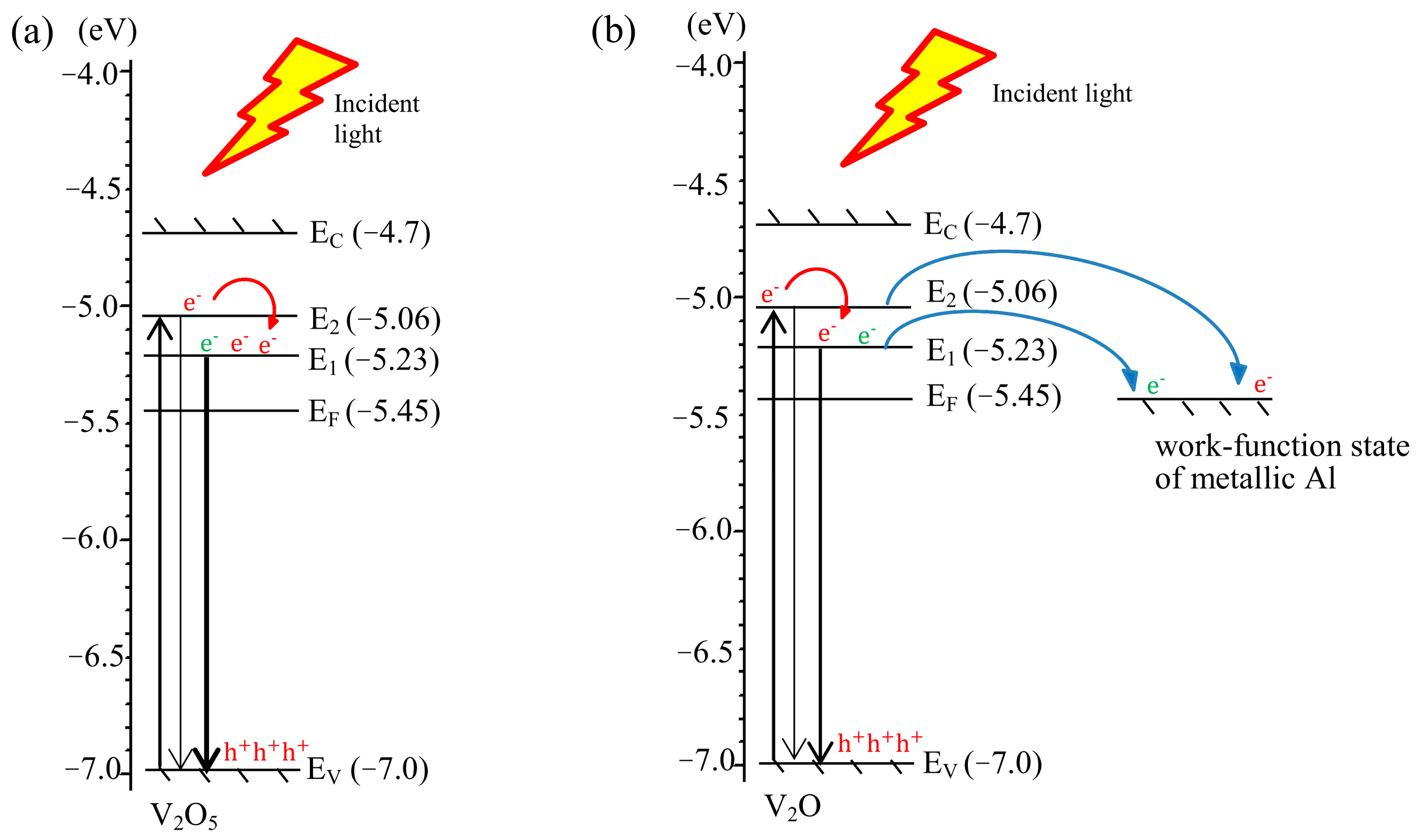
Figure 6 presents a possible mechanism for E1 and E2 from the AV NSs. The conduction band (EC), Fermi level (EF), and valence band (EV) of the V2O5 structures in the Al-free V2O5 NSs, are at −4.7, −5.45, and −7.00 eV [47], respectively, as shown in Figure 6a. Some of the excited electrons in the E1 level were generated by an incident light from the Ev of the V2O5 transiting to the E2 level, causing the intensity of E2 to exceed that of E1, as shown in Figure 5b. According to XPS and XRD results, the metallic Al exists in the V2O5 NSs, which can be located between the layered V2O5 structure and/or the oxygen vacancy. The Fermi level of the metallic Al is approximately 4.08–4.28 eV [48]. Hence, in the Al-doped V2O5 NSs, as shown in Figure 6b, these excited electrons in the E2 level, which were excited by the incident radiation, can transit along three pathways. These pathways are (1) from E2 to E1, and then to the Fermi level of the metallic Al; (2) from E2 to the work-function level of the metallic Al; and (3) from E2 to E1. Along pathway 1, the excited electrons transit to the metallic Al, so the E2 intensity decreases; along pathway 2, the electrons that are generated upon the formation of the -defects transit to the metallic Al, leading the decreasing E1 intensity; along pathway 3, the excited electrons in the E2 level transit to the E1 level, so the intensity of E2 is lower than that of E1 for all of the AV NSs. Moreover, the concentration of is reduced upon the addition of Al dopant because the sites of the defects are filled by Al0. Then the intensity of E1 emission thus tends to decrease. These results suggest that Al as the dopant plays the following three roles in the AV NSs system: (1) as an electron sink, (2) filling the sites of the defects and reducing the concentration, and (3) intercalating the layered V2O5 structure. Therefore, the intensity of E1 and E2 both decreases as the Al dopant concentration increases.
4. Conclusions
Both Al-free and Al-doped V2O5 NSs were fabricated on the Si (100) substrate by a thermally activated CVD process at 850 °C via a V-S mechanism. XPS revealed the V–O binding energy of the V2O5 phase and the presence of metallic Al rather than Al3+ ions. XRD revealed the typical orthorhombic phase of the V2O5 with c/a and c/b ratios that increase with the Al dopant concentration, suggesting that Al0 (radius = 1.43 Å) preferentially fills the (radius = 1.4 Å) sites owing to their similar sizes. The FWHM has a similar value with a deviation of ±2.9% upon the addition of Al dopant, indicating that Al does not affect the V2O5 crystal structure. HRTEM verified that the growth direction of both Al-free and Al-doped V2O5 NSs is in the [110]-direction. Raman shifts revealed slight deviations upon the addition of Al, indicating that the Al content does not affect the binding structure of the V2O5. The photoluminescence results proved that the emission intensities at 1.77 and 1.94 eV decreased by factors of 61.6% and 59.9%, respectively, as the concentration of Al dopant increases from 0 to 1.5 wt.%. The decrease in the luminescence intensities was attributable to the following causes: (1) Al dopants reduced the -defect concentration and (2) Al acted as an electron sink. Therefore, the recombination rate of electrons and holes decreases, reducing the luminescence intensities at 1.77 and 1.94 eV, upon doping with Al. Al-doped V2O5 NSs have potential applications in photocatalysts, solar cells, gas sensors, and electrodic materials.
Author Contributions
Conceptualization, H.C.S. and F.-S.S.; methodology, H.C.S., F.-S.S., C.-L.L. and C.-C.W.; software, C.-C.W. and C.-L.L.; validation, C.-C.W. and C.-L.L.; formal analysis, C.-C.W.; investigation, C.-C.W., and C.-L.L.; resources, H.C.S. and F.-S.S.; data curation, C.-C.W. and C.-L.L.; writing—original draft preparation, C.-C.W.; writing—review and editing, H.C.S. and F.-S.S.; visualization, C.-C.W. and C.-L.L.; supervision, H.C.S. and F.-S.S.; project administration, H.C.S.; funding acquisition, H.C.S. All authors have read and agreed to the published version of the manuscript.
Funding
This research was funded by the Ministry of Science and Technology (MOST) of Taiwan, Republic of China, grant number MOST 108-2221-E-034-010.
Institutional Review Board Statement
Not applicable.
Informed Consent Statement
Not applicable.
Data Availability Statement
Data is contained within the article.
Acknowledgments
The authors gratefully acknowledge the financial support of the Ministry of Science and Technology (MOST) of Taiwan.
Conflicts of Interest
The authors declare no conflict of interest.
References
- Liu, M.; Su, B.; Tang, Y.; Jiang, X.; Yu, A. Recent advances in nanostructured vanadium oxides and composites for energy conversion. Adv. Energy Mater. 2017, 7, 1–34. [Google Scholar]
- Surnev, S.; Ramsey, M.G.; Netzer, F.P. Vanadium oxide surface studies. Prog. Surf. Sci. 2003, 73, 117–165. [Google Scholar] [CrossRef]
- Lee, S.H.; Cheong, H.M.; Seong, M.J.; Liu, P.; Tracy, C.E.; Mascarenhas, A.; Pitts, J.R.; Deb, S.K. Raman spectroscopic studies of amorphous vanadium oxide thin films. Solid State Ion. 2003, 165, 111–116. [Google Scholar] [CrossRef]
- Sucharitakul, S.; Ye, G.; Lambrecht, W.R.L.; Bhandari, C.; Gross, A.; He, R.; Poelman, H.; Gao, X.P.A. V2O5: A 2D van der Waals oxide with strong in-plane electrical and optical anisotropy. ACS Appl. Mater. Interfaces 2017, 9, 23949–23956. [Google Scholar] [CrossRef] [PubMed]
- Chakrabarti, A.; Hermann, K.; Druzinic, R.; Witko, M.; Wagner, F.; Petersen, M. Geometric and electronic structure of vanadium pentoxido: A density functional bulk and surface study. Phys. Rev. B 1999, 59, 10583–10590. [Google Scholar] [CrossRef] [Green Version]
- Wang, Y.; Su, Q.; Chen, C.H.; Yu, M.L.; Han, G.J.; Wang, G.Q.; Xin, K.; Lan, W.; Liu, X.Q. Low temperature growth of vanadium pentoxide nanomaterials by chemical vapour deposition using VO (acac)2 as precursor. J. Phys. D Appl. Phys. 2010, 43, 185102. [Google Scholar] [CrossRef]
- Wang, C.C.; Lu, C.L.; Shieu, F.S.; Shih, H.C. Enhanced photoluminescence properties of Ga-Doped V2O5 nanorods via defect structures. Chem. Phys. Lett. 2020, 738, 136864. [Google Scholar] [CrossRef]
- Wang, C.C.; Chen, K.C.; Shieu, F.S.; Shih, H.C. Characterization and photoluminescence of V2O5@Pt core-Shell nanostructures as fabricated by atomic layer deposition. Chem. Phys. Lett. 2019, 729, 24–29. [Google Scholar] [CrossRef]
- Van, K.L.; Groult, H.; Mantoux, A.; Perrigaud, L.; Lantelme, F.; Lindstrom, R.; Badour-Hadjean, R.; Zanna, S.; Lincot, D. Amorphous vanadium oxide films synthesised by ALCVD for lithium rechargeable batteries. J. Power Sources 2006, 160, 592–601. [Google Scholar] [CrossRef]
- Venkatesan, A.; Chandar, N.R.K.; Pradeeswari, K.; Pandi, P.; Kandasamy, A.; Kumar, R.M.; Jayavel, R. Influence of Al doping on structural, luminescence and electrochemical properties of V2O5 nanostructures synthesized via non-Hydrolytic sol-Gel technique. Mater. Res. Express 2019, 6, 015017. [Google Scholar] [CrossRef]
- Díaz-Guerra, C.; Piqueras, J. Structural and cathodoluminescence assessment of V2O5 nanowires and nanotips grown by thermal deposition. J. Appl. Phys. 2007, 102, 084307. [Google Scholar] [CrossRef] [Green Version]
- Schlecht, U.; Knez, M.; Duppel, V.; Kienle, L.; Burghard, M. Boomerang-shaped VOX belts: Twinning within isolated nanocrystals. Appl. Phys. A: Mater. Sci. Process. 2004, 78, 527. [Google Scholar] [CrossRef]
- González-Rivera, Y.A.; Cervantes-Juárez, E.; Aquino-Meneses, L.; Lozada-Morales, R.; Jiménez-Sandoval, S.; Rubio-Rosas, E.; Agustín-Serrano, R.; de la Cerna, C.; Reyes-Cervantes, E.; Zelaya Angel, O.; et al. Photoluminescence in Er-Doped V2O5 and Er-doped CdV2O6. J. Lumin. 2014, 155, 119–124. [Google Scholar] [CrossRef]
- Suresh, R.; Giribabu, K.; Manigandan, R.; Munusamy, S.; Kumar, S.P.; Muthamizh, S.; Stephen, A.; Narayanan, V. Doping of Co into V2O5 nanoparticles enhances photodegradation of methylene blue. J. Alloys Compd. 2014, 598, 151–160. [Google Scholar] [CrossRef]
- Aquino-Meneses, L.; Lozada-Morales, R.; del Angel-Vicente, P.; Percino-Picazo, J.C.; Zelaya-Angel, O.; Becerril, M.; Carmona-Rodriguez, J.; Rodriguez-Melgarejo, F.; Jime’nez-Sandoval, S. Photoluminescence in Nd-Doped V2O5. J. Mater. Sci. 2014, 49, 2298–2302. [Google Scholar] [CrossRef]
- Venkatesan, A.; Chandar, N.R.K.; Kandasamy, A.; Chinnu, M.K.; Marimuthu, K.N.; Kumar, R.M.; Jayavel, R. Luminescence and electrochemical properties of rare earth (Gd, Nd) doped V2O5 nanostructures synthesized by a non-Aqueous sol-Gel route. RSC Adv. 2015, 5, 21778. [Google Scholar] [CrossRef]
- Azevedo, C.F.; Balboni, R.D.C.; Cholant, C.M.; Moura, E.A.; Lemos, R.M.J.; Pawlicka, A.; Gündel, A.; Flores, W.H.; Pereira, M.; Avellaneda, C.O. New thin films of NiO doped with V2O5 for electrochromic Applications. J. Phys. Chem. Solids 2017, 110, 30–35. [Google Scholar] [CrossRef]
- Ongul, F. Solution-Processed inverted organic solar cell using V2O5 hole transport layer and vacuum free EGaIn anode. Opt. Mater. 2015, 50, 244–249. [Google Scholar] [CrossRef]
- Alsulami, A.; Griffin, J.; Alqurashi, R.; Yi, H.; Iraqi, A.; Lidzey, D.; Buckley, A. Thermally stable solution processed vanadium oxide as a hole extraction layer in organic solar cells. Materials 2016, 9, 235. [Google Scholar] [CrossRef] [Green Version]
- Zhao, W.; Zhong, Q.; Pan, Y.; Zhang, R. Defect structure and evolution mechanism of O2− radical in F-Doped V2O5/TiO2 catalysts. Colloids Surf. A: Physicochem. Eng. Asp. 2013, 436, 1013–1020. [Google Scholar] [CrossRef]
- Pandey, G.P.; Liu, T.; Brown, E.; Yang, Y.; Li, Y.; Sun, X.S.; Fang, Y.; Li, J. Mesoporous hybrids of reduced graphene oxide and vanadium pentoxide for enhanced performance in lithium-Ion batteries and electrochemical capacitors. ACS Appl. Mater. Interfaces 2016, 8, 9200–9210. [Google Scholar] [CrossRef]
- Mane, A.A.; Suryawanshi, M.P.; Kim, J.H.; Moholkar, A.V. Superior selectivity and enhanced response characteristics of palladium sensitized vanadium pentoxide nanorods for detection of nitrogen dioxide gas. J. Colloid Interface Sci. 2017, 495, 53–60. [Google Scholar] [CrossRef] [PubMed]
- Ghanei-Motlagh, M.; Taher, M.A.; Fayazi, M.; Baghayeri, M.; Hosseinifar, A. Non-Enzymatic amperometric sensing of hydrogen peroxide based on vanadium pentoxide nanostructures. J. Electrochem. Soc. 2019, 166, B367–B372. [Google Scholar] [CrossRef]
- Pradeep, I.; Kumar, E.R.; Suriyanarayanan, N.; Mohanraj, K.; Srinivas, C.; Mehar, M.V.K. Effect of Al doping concentration on the structural, optical, morphological and electrical properties of V2O5 nanostructures. New J. Chem. 2018, 42, 4278. [Google Scholar] [CrossRef]
- Venkatesan, A.; Chandar, N.K.; Kumar, M.K.; Arjunan, S.; Kumar, R.M.; Jayavel, R. Al3+ Doped V2O5 Nanostructure: Synthesis and Structural, Morphological and Optical Characterization. In Proceedings of the AIP Conference, Mumbai, India, 3–7 December 2012; Volume 1512, p. 392. [Google Scholar]
- Ali, H.M.; Hakeem, A.M.A. Structural and optical properties of electron-Beam evapo-Rated Al2O3-Doped V2O5 thin films for various applications. Phys. Status Solidi A 2010, 207, 132–138. [Google Scholar] [CrossRef]
- De Jesus, L.R.; Horrocks, G.A.; Liang, Y.; Parija, A.; Jaye, C.; Wangoh, L.; Wang, J.; Fischer, D.A.; Piper, L.F.J.; Prendergast, D.; et al. Mapping polaronic states and lithiation gradients in individual V2O5 nanowires. Nat. Commun. 2016, 7, 12022. [Google Scholar] [CrossRef] [Green Version]
- Wu, Q.H.; Thissen, A.; Jaegermann, W.; Liu, M. Photoelectron spectroscopy study of oxygen vacancy on vanadium oxides surface. Appl. Surf. Sci. 2004, 236, 473–478. [Google Scholar] [CrossRef]
- Silversmit, G.; Depla, D.; Poelman, H.; Marin, G.B.; De Gryse, R. Determination of the V2p XPS binding energies for different vanadium oxidation states (V5+ to V0+). J. Electron Spectrosc. Relat. Phenom. 2004, 135, 167–175. [Google Scholar] [CrossRef]
- Harris, D.C. Quantitative Chemical Analysis, 7th ed.; W.H. Freeman: New York, NY, USA, 2007. [Google Scholar]
- Sun, C.; Zeng, R.; Zhang, J.; Qiu, Z.J.; Wu, D. Effects of UV-Ozone treatment on sensing behaviours of EGFETs with Al2O3 sensing film. Materials 2017, 10, 1432. [Google Scholar] [CrossRef] [Green Version]
- Wagner, C.D.; Riggs, W.M.; Davis, L.E.; Mullenberg, J.F. Handbook of X-ray Photoelectron Spectroscopy; Perkin-Elmer Corporation: Waltham, MA, USA, 1979; p. 50. [Google Scholar]
- Murugan, A.V.; Kale, B.B.; Kwon, C.W.; Campet, G.; Vijayamohanan, K. Synthesis and characterization of a new organo–inorganic poly (3,4-ethylene dioxythiophene) PEDOT/V2O5 nanocomposite by intercalation. J. Mater. Chem. 2001, 11, 2470–2475. [Google Scholar] [CrossRef]
- Singh, B.; Gupta, M.K.; Mishra, S.K.; Mittal, R.; Sastry, P.U.; Rols, S.; Chaplot, S.L. Anomalous lattice behavior of vanadium pentaoxide (V2O5): X-ray diffraction, inelastic neutron scattering and ab initio lattice dynamics. Phys. Chem. Chem. Phys. 2017, 19, 17967–17984. [Google Scholar] [CrossRef] [PubMed] [Green Version]
- Shen, W.J.; Sun, K.W.; Lee, C.S. Electrical characterization and Raman spectroscopy of individual vanadium pentoxide nanowire. J. Nanoparticle Res. 2011, 13, 4929–4936. [Google Scholar] [CrossRef]
- Dewangan, K.; Sinha, N.N.; Chavan, P.G.; Sharma, P.K.; Pandey, A.C.; More, M.A.; Joag, D.S.; Munichandraiah, N.; Gajbhiye, N.S. Synthesis and characterization of self-Assembled nanofiber-bundles of V2O5: Their electrochemical and field emission properties. Nanoscale 2012, 4, 645–651. [Google Scholar] [CrossRef] [PubMed] [Green Version]
- Urena-Begar, F.; Crunteanu, A.; Raskin, J.P. Raman and XPS characterization of vanadium oxide thin films with temperature. Appl. Surf. Sci. 2017, 403, 717–727. [Google Scholar] [CrossRef]
- Baddour-Hadjean, R.; Pereira-Ramos, J.P. Raman microspectrometry applied to the study of electrode materials for lithium batteries. Chem. Rev. 2010, 110, 1278–1319. [Google Scholar] [CrossRef]
- Baddour-Hadjean, R.; Golabkan, V.; Pereira-Ramos, J.P.; Mantoux, A.; Lincot, D. A Raman study of the lithium insertion process in vanadium pentoxide thin films deposited by atomic layer deposition. J. Raman Spectrosc. 2002, 33, 631–638. [Google Scholar] [CrossRef]
- Liu, X.; Huang, C.; Qiu, J.; Wang, Y. The effect of thermal annealing and laser irradiation on the microstructure of vanadium oxide nanotubes. Appl. Surf. Sci. 2006, 253, 2747–2751. [Google Scholar] [CrossRef]
- Chen, W.; Mai, L.; Peng, J.; Xu, Q.; Zhu, Q. Raman spectroscopic study of vanadium oxide nanotubes. J. Solid State Chem. 2004, 177, 377–379. [Google Scholar] [CrossRef]
- Jung, H.; Gerasopoulos, K.; Alec Talin, A.; Ghodssi, R. A platform for in situ Raman and stress characterizations of V2O5 cathode using MEMS device. Electrochim. Acta 2017, 242, 227–239. [Google Scholar] [CrossRef]
- Al-Assiri, M.S.; El-Desoky, M.M.; Alyamani, A.; Al-Hajry, A.; Al-Mogeeth, A.; Bahgat, A.A. Structural and transport properties of Li-intercalated vanadium pentoxide nanocrystalline films. Philos. Mag. 2010, 90, 3421–3439. [Google Scholar] [CrossRef]
- Park, Y.; Kim, N.H.; Kim, J.Y.; Eom, I.Y.; Jeong, Y.U.; Kim, M.S.; Lee, S.M.; Choi, H.C.; Jung, Y.M. Surface characterization of the high voltage LiCoO2/Li cell by X-ray photoelectron spectroscopy and 2D correlation analysis. Vib. Spectrosc. 2010, 53, 60–63. [Google Scholar] [CrossRef]
- Milewska, A.; Świerczek, K.; Tobola, J.; Boudoire, F.; Hu, Y.; Bora, D.K.; Mun, B.S.; Braun, A.; Molenda, J. The nature of the nonmetal–Metal transition in LixCoO2 oxide. Solid State Ionics 2014, 263, 110–118. [Google Scholar] [CrossRef]
- Faggio, G.; Modafferi, V.; Panzera, G.; Alfieri, D.; Santangelo, S. Micro-Raman and photoluminescence analysis of composite vanadium oxide/poly-Vinyl acetate fibres synthesised by electro-Spinning. J. Raman Spectrosc. 2012, 43, 761–768. [Google Scholar] [CrossRef]
- Gurulakshmi, M.; Selvaraj, M.; Selvamani, A.; Vijayan, P.; Sasi Rekha, N.R.; Shanthi, K. Enhanced visible-Light photocatalytic activity of V2O5/S-TiO2 nanocomposites. Appl. Catal. A Gen. 2012, 449, 31–46. [Google Scholar] [CrossRef]
- Kumar, B.; Kaushik, B.K.; Negi, Y.S. Perspectives and challenges for organic thin film transistors: Materials, devices, processes and applications. J. Mater. Sci: Mater. Electron. 2014, 25, 1–30. [Google Scholar]
Figure 1.
X-ray photoelectron spectroscopy (XPS) spectra of V 2p and O 1s of (a) AV0 and AV15 NSs (Al-doped V2O5 nanostructures). (b) Al 2p of AV NSs.
Figure 1.
X-ray photoelectron spectroscopy (XPS) spectra of V 2p and O 1s of (a) AV0 and AV15 NSs (Al-doped V2O5 nanostructures). (b) Al 2p of AV NSs.

Figure 2.
(a) Powder X-ray diffraction (XRD) analysis of AV NSs and the inset showing FWHMs varying Al dopants in V2O5 (001); (b) c/a and c/b ratios varying with Al dopant (wt.%); the inset depicting the V2O5 molecular structures [34].
Figure 2.
(a) Powder X-ray diffraction (XRD) analysis of AV NSs and the inset showing FWHMs varying Al dopants in V2O5 (001); (b) c/a and c/b ratios varying with Al dopant (wt.%); the inset depicting the V2O5 molecular structures [34].

Figure 3.
Field-emission scanning electron microscopy (FESEM) images of (a) AV0 and (b) AV10 nanostructures. High-resolution transmission electron microscopy (HRTEM) images of (c) AV0 and (d) AV10 NSs, Insets 1 and 3 showing the high resolution images of the AV0 and AV10 NSs, respectively; while inset 2 and 4 showing the SAD pattern of the AV0 and AV10 NSs.

Figure 5.
(a) Photoluminescence (PL) spectra of the samples AV0, AV05, AV10, and AV15 NSs; and (b) intensities of the E1 and E2 varying with the Al contents.
Figure 5.
(a) Photoluminescence (PL) spectra of the samples AV0, AV05, AV10, and AV15 NSs; and (b) intensities of the E1 and E2 varying with the Al contents.
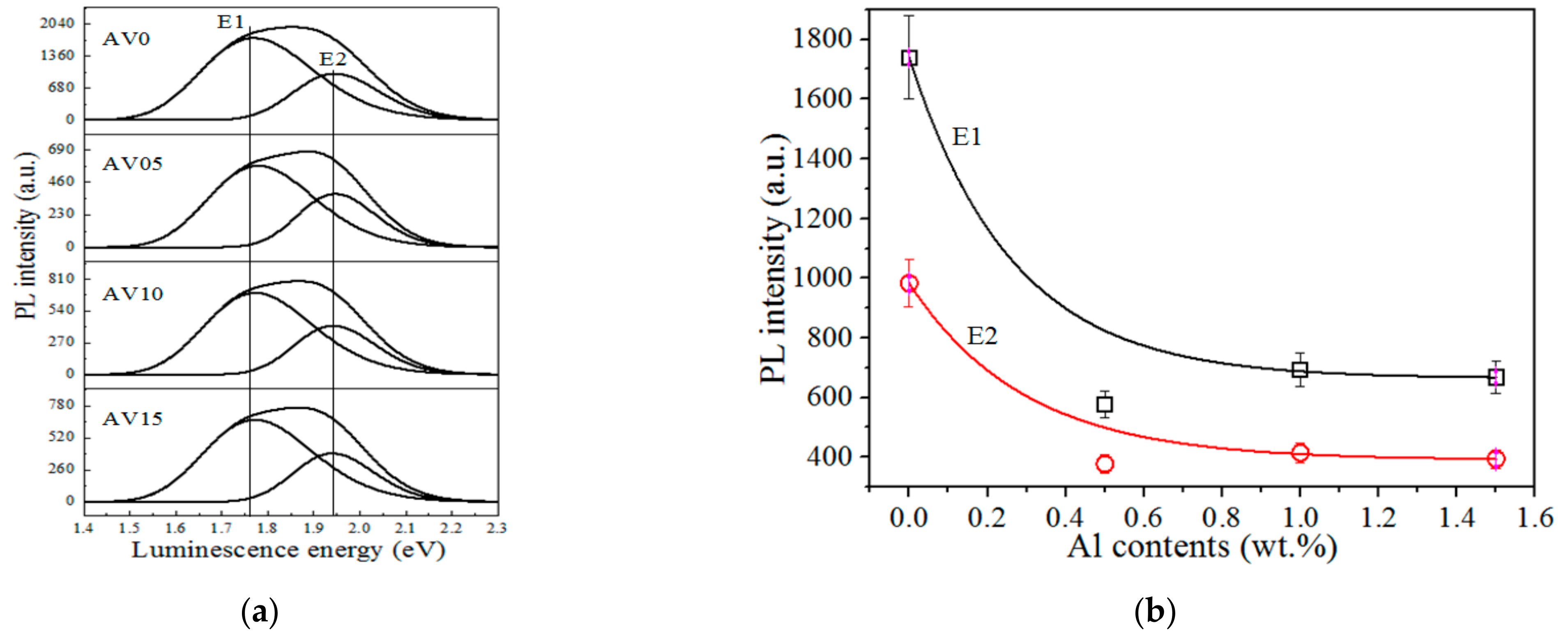
Figure 6.
Proposed mechanism of the migration pathways for the electrons and holes in (a) Al-free and (b) Al-doped V2O5 NSs at an equilibrium state.
Figure 6.
Proposed mechanism of the migration pathways for the electrons and holes in (a) Al-free and (b) Al-doped V2O5 NSs at an equilibrium state.

Table 1.
Al at.% of the AV NSs with various Al contents (wt.%).
| Samples | AV0 | AV05 | AV10 | AV15 |
|---|---|---|---|---|
| Al contents(g) | 0 | 0.0015 | 0.003 | 0.0045 |
| Al contents (wt.%) | 0 | 0.5 | 1 | 1.5 |
| Al contents (at.%) | 0 | 4.45 | 8.64 | 11.31 |
Table 2.
Lattice constants, c/a, and c/b of the AV NSs with various Al contents.
| Al Contents (wt.%) | Diffraction Angle (2θ) | Lattice Constants of V2O5 (Å) | c/a | c/b | ||||
|---|---|---|---|---|---|---|---|---|
| V2O5 (001) | V2O5 (110) | V2O5(400) | a | b | c | |||
| 0 | 20.36 | 26.17 | 31.07 | 11.504 | 3.562 | 4.357 | 0.3787 | 1.2234 |
| 0.5 | 20.42 | 26.28 | 31.19 | 11.461 | 3.546 | 4.345 | 0.3791 | 1.2253 |
| 1.0 | 20.35 | 26.19 | 31.10 | 11.492 | 3.558 | 4.361 | 0.3795 | 1.2256 |
| 1.5 | 20.33 | 26.19 | 31.09 | 11.494 | 3.558 | 4.363 | 0.3842 | 1.2263 |
Table 4.
The influence in PL intensities of V2O5 in various dopant precursors.
| Dopant Precursors | Dopant Type | PL Intensity of the V2O5 | Ref. |
|---|---|---|---|
| metallic Al | Al0 | Decreases with the increasing precursor contents | This work |
| metallic Ga | Ga3+ | Enhancement at proper precursor contents | [7] |
| Al(NO3)3·9H2O | Al3+ | Decreases with the increasing precursor contents | [10] |
| Er(NO3)3·5H2O | Er3+ | No data | [13] |
| CoSO4·7H2O | Co2+ | Decreases with the increasing precursor contents | [14] |
| Gd2O3 | Gd3+ | Decreases with the adding of precursor | [16] |
| Nd2O3 | Nd3+ | Decreases with the adding of precursor | [16] |
| Al(NO3)3 | Al3+ | Decreases with the adding of precursor | [24] |
Publisher’s Note: MDPI stays neutral with regard to jurisdictional claims in published maps and institutional affiliations. |
© 2021 by the authors. Licensee MDPI, Basel, Switzerland. This article is an open access article distributed under the terms and conditions of the Creative Commons Attribution (CC BY) license (http://creativecommons.org/licenses/by/4.0/).
Share and Cite
MDPI and ACS Style
Wang, C.-C.; Lu, C.-L.; Shieu, F.-S.; Shih, H.C. Structure and Photoluminescence Properties of Thermally Synthesized V2O5 and Al-Doped V2O5 Nanostructures. Materials 2021, 14, 359. https://doi.org/10.3390/ma14020359
AMA Style
Wang C-C, Lu C-L, Shieu F-S, Shih HC. Structure and Photoluminescence Properties of Thermally Synthesized V2O5 and Al-Doped V2O5 Nanostructures. Materials. 2021; 14(2):359. https://doi.org/10.3390/ma14020359
Chicago/Turabian StyleWang, Chih-Chiang, Chia-Lun Lu, Fuh-Sheng Shieu, and Han C. Shih. 2021. "Structure and Photoluminescence Properties of Thermally Synthesized V2O5 and Al-Doped V2O5 Nanostructures" Materials 14, no. 2: 359. https://doi.org/10.3390/ma14020359
Note that from the first issue of 2016, this journal uses article numbers instead of page numbers. See further details here.