
A Review of β-Ga2O3 Power Diodes

1
School of Microelectronics, Fudan University, Shanghai 200433, China
2
National Integrated Circuit Innovation Center, Shanghai 201203, China
*
Author to whom correspondence should be addressed.
Materials 2024, 17(8), 1870; https://doi.org/10.3390/ma17081870
Submission received: 29 March 2024
/
Revised: 15 April 2024
/
Accepted: 15 April 2024
/
Published: 18 April 2024
(This article belongs to the Special Issue Advanced Semiconductor/Memory Materials and Devices)
Abstract
:As the most stable phase of gallium oxide, β-Ga2O3 can enable high-quality, large-size, low-cost, and controllably doped wafers by the melt method. It also features a bandgap of 4.7–4.9 eV, a critical electric field strength of 8 MV/cm, and a Baliga’s figure of merit (BFOM) of up to 3444, which is 10 and 4 times higher than that of SiC and GaN, respectively, showing great potential for application in power devices. However, the lack of effective p-type Ga2O3 limits the development of bipolar devices. Most research has focused on unipolar devices, with breakthroughs in recent years. This review mainly summarizes the research progress fora different structures of β-Ga2O3 power diodes and gives a brief introduction to their thermal management and circuit applications.
1. Introduction
As technology advances, there is an increasing need for electronic devices capable of a high frequency, high voltage, and high power in various applications, such as AI, 5G communication, electric vehicles, rail transportation, new energy power generation, and power transmission [1,2,3,4]. Si, being the most mature semiconductor material, is widely used in electronic manufacturing, but its narrow bandgap (1.12 eV) significantly limits its application in high-voltage fields. Si-based power devices are gradually reaching their performance limits but still cannot meet the growing demands for development [5,6,7]. Consequently, wide-bandgap semiconductor materials, represented by SiC (3.3 eV) and GaN (3.4 eV), have progressively entered the spotlight. Owing to their larger bandgap, the device’s maximum breakdown field strength can be improved, and their higher electron mobility and saturation velocity result in lower conduction losses and switching losses. Hence, wide-bandgap power semiconductor devices have witnessed a rapid development, serving to address the shortcomings of Si-based power devices in the field of high-power electronics [8,9]. However, the production cost of SiC and GaN is significantly higher than that of Si wafers, as these materials require epitaxial growth methods to obtain high-quality crystals, which severely limits their large-scale application [10,11,12].
As a quintessential exemplar of ultra-wide-bandgap semiconductors, Ga2O3 manifests in five polymorphic phase structures, encompassing the α, β, γ, δ, and ε phases. Among them, the β phase is endowed with thermodynamic stability. Utilizing melt growth methodologies, it is feasible to fabricate high-quality, large-scale, cost-effective, and doping-controllable β-Ga2O3 wafers. Furthermore, several pivotal electrical properties of β-Ga2O3 exhibit superiority over those inherent to SiC and GaN [13,14,15,16,17,18,19]. Currently, 6-inch β-Ga2O3 wafers have been successfully fabricated using the edge-defined film-fed growth (EFG) technique. The cost of β-Ga2O3 wafers produced via the Czochralski (CZ) method amounts to only one-third of that for SiC wafers of the same size. Notably, the EFG method proves even more cost-effective, being two times less expensive than the CZ process, thus rendering the overall cost of β-Ga2O3 substantially lower than that of SiC [20,21]. Moreover, during the production of β-Ga2O3 wafers, the cost and attrition rate of Ir crucibles constitute a significant proportion of expenditure. In April 2022, C&A Corporation (Sendai, Japan) succeeded in growing 2-inch β-Ga2O3 single crystals using a Cu crucible CZ method, potentially reducing costs to one-hundredth of those associated with the EFG method, laying the foundation for the mass application of β-Ga2O3 devices [22]. Electrically, β-Ga2O3 possesses a wider bandgap of 4.7–4.9 eV and a critical electric field strength of 8 MV/cm, which is 27 times that of Si, 3 times that of SiC, and 2 times that of GaN. The Baliga’s figure of merit (BFOM), a crucial parameter for evaluating the suitability of materials for power device fabrication, reaches 3444 for β-Ga2O3, which is 10 times that of SiC and 4 times that of GaN; this indicates that β-Ga2O3 possesses greater potential for application in power devices [23,24,25,26].
Although β-Ga2O3 offers the advantages of low cost and high performance, similar to other wide-bandgap semiconductor materials, it is challenging to obtain p-type Ga2O3 with a high conductivity [27,28,29,30]. Calculations suggest the absence of shallow acceptors in Ga2O3, and holes exhibit self-trapping effects within the material [31,32]. Consequently, current research is primarily focused on unipolar Ga2O3 power electronic devices, including field-effect transistors (FETs) and Schottky barrier diodes (SBDs) [33,34,35]. Compared to traditional p-n junction diodes, SBDs exhibit lower turn-on voltages and faster recovery times, making them commonly employed in low-power and high-speed switching applications. However, the breakdown voltage (BV) of conventional Si-based SBDs is generally low, and the introduction of wide-bandgap materials can effectively elevate their breakdown limits. Since Sasaki et al. [36] first reported on β-Ga2O3 SBDs in 2012, β-Ga2O3 SBD devices have been developing towards a higher BV and lower on-resistance (Ron) through improvements in epitaxial layer quality, device structure enhancements, and optimized manufacturing processes.
In recent years, there has been a sharp increase in research publications on Ga2O3 SBDs, leading to significant breakthroughs in device performance. Lateral β-Ga2O3 SBDs have achieved a BV exceeding 10 kV [37,38], and vertical NiO/β-Ga2O3 Schottky heterojunction diodes devices have reached a power figure of merit (PFOM = BV2/Ron) of 13.2 GW/cm2 [39]. Significant progress has also been made in commercial applications; in December 2021, Novel Crystal Technology Inc. (Saitama, Japan) announced the release of an ampere-level 1200 V β-Ga2O3 trench SBD device [40]. Therefore, it is essential to compile a summary of the current research progress on β-Ga2O3 power SBD devices, as it may provide meaningful guidance for future developments in the field.
This article provides a comprehensive review of the research advancements in variously structured β-Ga2O3 power SBDs up to the year 2024. Section 2 elucidates the material properties of β-Ga2O3, substrate preparation, and epitaxial processes; Section 3 discusses the metal/β-Ga2O3 contacts, including ohmic and Schottky contacts; Section 4 presents the progress in research on differently structured β-Ga2O3 power diodes, which encompasses vertical structure SBDs, heterojunction structure diodes, and lateral structure diodes; Section 5 offers a brief overview of the surge current robustness and thermal management of β-Ga2O3 SBD devices; Section 6 summarizes the circuit applications and reliability of β-Ga2O3 SBDs; and Section 7 concludes with a summary and prospects.
2. β-Ga2O3 Materials
Ga2O3 material can exist in five crystal phases (α, β, γ, δ, and ε), among which the monoclinic β-Ga2O3 phase prevails instability. The remaining four phases are metastable and can be converted to β-Ga2O3 under certain conditions, as depicted in Figure 1 [13,14]. Notably, β-Ga2O3 exhibits commendable thermal and physicochemical stability, making it the most extensively studied phase to date. The α-Ga2O3 phase possesses a corundum structure and is typically grown heteroepitaxial on sapphire substrates [41,42,43,44], making it the second-most researched phase. The FLOSFIA company (Kyoto, Japan) predominantly employs Mist-epitaxy to prepare α-Ga2O3 wafers, and in March 2023, they unveiled an amperage-class 1700 V α-Ga2O3 trench SBD device [45,46,47,48,49]. The cubic spinel structure of γ-Ga2O3 is principally utilized as a photocatalyst for hydrogen production via water splitting [50,51,52,53]. Current research on the cubic perovskite structure of δ-Ga2O3 is comparatively limited. The hexagonal structure of ε-Ga2O3, which exhibits spontaneous polarization, can form a high-density two-dimensional electron gas at heterojunction interfaces and holds the potential for fabricating high-electron-mobility transistors [54,55]. Furthermore, there exists an orthorhombic κ-Ga2O3 with a very similar crystal-structure ε-Ga2O3, and they are usually considered as one structure [56,57]. Recently, orthorhombic κ-Ga2O3 has been proven to be stable up to 800–1000 °C, and this makes it suitable for the fabrication of reliable devices such as detectors for UV and X-rays [58,59,60,61].
Monoclinic-phase β-Ga2O3 belongs to the C2/m space group with a densely stacked anion structure. Its crystal structure and unit cell schematic are shown in Figure 2 [19,62]. The unit cell is comprised of two GaO4 tetrahedra and two GaO6 octahedra, containing two different Ga atomic positions, as well as three distinct O atomic sites. The lattice constants of β-Ga2O3 are as follows: a = 12.21 Å, b = 3.03 Å, c = 5.79 Å, with α = γ = 90° and β = 103.8°. The length of the a-axis is four times that of the b-axis, and the length of the c-axis is 1.9 times that of the b-axis, which facilitates cleavage along the (100) and (001) directions. Utilizing these crystallographic properties of β-Ga2O3, it is feasible to perform mechanical exfoliation to create quasi-two-dimensional thin-layer materials. This attribute endows β-Ga2O3 with significant potential in the domain of two-dimensional materials and devices [63,64,65,66].
The growth techniques for β-Ga2O3 single-crystal substrates predominantly encompass the Czochralski method (CZ) [15,18,67], optical floating zone method (OFZ) [68,69,70], vertical Bridgman method (VB) [71,72,73], and edge-defined film-fed growth method (EFG) [17,74,75,76,77], among which the EFG is the most mature, offering the potential for mass production and cost efficiency. In 2018, Japan’s Novel Crystal Technology Inc. (Saitama, Japan) pioneered the fabrication of 6-inch β-Ga2O3 single-crystal substrates using the EFG method. The company has also industrialized the production of 4-inch β-Ga2O3 single-crystal substrates, currently holding an international leading position, thereby laying the foundation for the large-scale commercialization of gallium oxide devices.
Advancements in substrate materials have also facilitated the development of β-Ga2O3 homoepitaxial film technologies. The epitaxial techniques widely employed today include molecular beam epitaxy (MBE) [78,79,80], halide vapor phase epitaxy (HVPE) [81,82,83,84], metal–organic chemical vapor deposition (MOCVD) [85,86,87], pulsed laser deposition (PLD) [88,89,90], low-pressure chemical vapor deposition (LPCVD) [91,92,93], and mist chemical vapor deposition (Mist-CVD) [43,94,95]. Among these, HVPE has been distinguished for achieving high growth rates of approximately 28 µm/h for epitaxial films. It also allows for precise doping concentration control within the range of 1015 to 1019 cm−3. At present, the majority of the commercially produced β-Ga2O3 single-crystal epitaxial layers are fabricated utilizing HVPE technology.
As compared to the already implemented SiC and GaN, the β-Ga2O3 material exhibits superior properties, as shown in Table 1 [19,96]. The bandgap of β-Ga2O3 ranges from 4.7 to 4.9 eV, with its ultraviolet absorption edge situated between 260 nm and 280 nm, precisely aligning with the solar-blind UV spectrum of 200 nm to 280 nm. This intrinsic property renders β-Ga2O3 a rare and ideally suited material for solar-blind UV detection. Consequently, Ga2O3-based solar-blind UV photodetectors have been extensively investigated [97,98,99,100]. Furthermore, β-Ga2O3 features a maximum critical electric field strength of up to 8 MV/cm and a BFOM of 3444. This implies that β-Ga2O3 devices have the theoretical capability to withstand a higher BV and operate under higher power conditions, making them more suitable for power device applications. Although diamond has superior properties in comparison, it is still far from being commercially viable, due to the limit of its large size and high-quality single crystal preparation, as well as its extremely high production and processing costs [101,102]. Interestingly, diamond is capable of effective p-type doping but lacks n-type doping and possesses a very high thermal conductivity. Thus, the complementary formation of a heterojunction diode with β-Ga2O3 can give full play to the advantages of both. A diamond/β-Ga2O3 pn heterojunction diode with on/off ratios of greater than 108 at ±10 V and leakage currents of less than 10−12 A has already been obtained by a direct bonding method [103,104].
At present, Ga2O3 materials still lack effective p-type doping, and research applications are basically n-Ga2O3, typically doping with elements like Si and Sn within a range of 1015 to 1019 cm−3 in concentration. In recent years, researchers have begun to address the shortfall of p-type Ga2O3 by using p-type NiO to form a p-n heterojunction with Ga2O3, presenting a novel approach for the advancement of Ga2O3 devices [39,105]. Besides, the primary challenges associated with β-Ga2O3 materials are their relatively low electron mobility and thermal conductivity. β-Ga2O3 exhibits an electron mobility of 300 cm2/V·s compared to GaN, rendering it less ideal for the fabrication of high-frequency devices. However, its saturation electron velocity of 2 × 107 cm/s offsets this disadvantage [106,107]. In response to potential heat dissipation issues due to the limited thermal conductivity of Ga2O3 materials, numerous studies have proposed solutions, such as hetero-bonding, substrate thinning, and junction-side cooling, which will be elaborated in Section 5. Overall, Ga2O3 devices possess considerable practical application value and hold broad prospects for utilization.
3. Metal/β-Ga2O3 Contact
The fundamental structure of β-Ga2O3 SBDs is composed of β-Ga2O3 and an anodic Schottky contact, as well as a cathodic ohmic contact. The contact between metal and β-Ga2O3 is the principal determinant of interfacial electron transport and significantly impacts the performance of the device.
3.1. Schottky Contact
When the metal and semiconductor are in contact, the diffusion of charge carriers equalizes the Fermi levels on both sides of the interface, reaching an equilibrium state. Consequently, after contact, the energy bands in the semiconductor become bent due to the built-in electric field, thereby forming an electron potential barrier at the interface, known as the Schottky barrier, as illustrated in Figure 3 [108]. The Mott model posits that the height of the Schottky barrier is solely related to the metal work function and the electron affinity of the semiconductor, and the Schottky barrier height (SBH) is equal to the difference between the two [109]. Experimentally, the SBH is commonly determined through current–voltage (I-V) or capacitance–voltage (C-V) measurements. Currently, there are many metals that are capable of forming Schottky contacts with β-Ga2O3, including Pt, Ir, Pd, Au, Ni, Co, Ru, Cu, Mo, W, Cr, Ti, Ag, etc.; graphite also forms Schottky contacts with β-Ga2O3. Among these, Ni is widely used, due to its low cost and ability to form excellent Schottky contacts with β-Ga2O3 [110,111,112,113].
However, experimental results indicate that the SBH of β-Ga2O3 weakly depends on the metal work function and is more influenced by interface states, as well as interface structures and interactions [114]. The Bardeen model suggests that electron transfer from the semiconductor to the metal is mediated by interface states on the contact surface, assuming a continuous distribution of surface states defined by a neutral energy level Φ0, with the Fermi level position determined by the location of the surface states within the bandgap, which is the Fermi level pinning effect [115]. Therefore, the surface states of β-Ga2O3 also significantly affect device performance; experiments have found that treatments such as oxygen plasma and annealing, as well as chemical solution cleaning, can effectively reduce the density of surface states on β-Ga2O3, enhancing device performance, while etching and plasma bombardment may increase surface state density, leading to poorer device performance [116,117,118,119,120,121].
In practical applications, due to the amount of heat generated by high power, power devices often operate in high-temperature environments, and many studies have investigated the high-temperature performance of different Schottky metal/β-Ga2O3 SBDs [122,123,124]. Furthermore, given that metal oxides have a better high-temperature stability and higher SBH compared to metals, β-Ga2O3 SBDs utilizing metal oxides as Schottky electrodes have also been the subject of extensive research [125,126,127]. Hou et al. [128] reported that IrOx/β-Ga2O3 Schottky contacts achieved a leakage current of only 2.3 × 10⁻⁹ A/cm2 (@-3 V) at a high temperature of 350 °C and just 7.5 × 10⁻⁸ A/cm2 at −100 V, with the rectification ratio exceeding 1010 at all temperatures. Dela Cruz et al. [129] showed the outstanding high-temperature performance of PtxIr(1−x)Oy on (01) β-Ga2O3, with a rectification ratio of 109 (±3 V) at 300 °C and 106 at 500 °C, demonstrating the application potential of metal oxide Schottky contacts in high-temperature devices.
3.2. Ohmic Contact
Typically, an excellent ohmic contact exhibits a low or even no SBH, manifesting a linear I-V curve that minimizes thermal effects caused by contact resistance. This is particularly crucial for β-Ga2O3, which has a low thermal conductivity. Hence, superior β-Ga2O3 ohmic contacts are a prerequisite for achieving high-performance devices. Currently, almost all Ga2O3 devices use Ti as the ohmic contact and deposit Au as a protective layer to avoid oxidation. The ohmic contacts can be effectively formed by heavy doping, plasma treatment, and post-annealing treatment [110,111,112,113]. In 2012, Higashiwaki et al. [130] first reported a field-effect transistor based on β-Ga2O3, utilizing Ti/Au ohmic contacts, and highlighted the necessity of Reactive Ion Etching (RIE) processing for establishing ohmic contacts. Subsequently, the ohmic contact of Ti on β-Ga2O3 was improved in β-Ga2O3 MOSFETs devices through annealing at 470 °C for 1 min [131]. Bhattacharyya et al. [132] reported a record low contact resistivity of 80 mΩ·mm for Ti metal on heavily doped (∼1.8 × 1020 cm−3) β-Ga2O3, with a specific contact resistivity of 8.3 × 10⁻⁷ Ω·cm2. Currently, the formation of high-quality Ti/β-Ga2O3 ohmic contacts is commonly achieved using post-annealing treatment.
4. β-Ga2O3 Power Diodes
In the last decade, β-Ga2O3 power diodes have been extensively studied due to their exceptional electrical properties. To enhance device performance, researchers have proposed new device structures, which can be categorized into three main groups based on their structure type: vertical-structure SBDs, vertical heterojunction-structure diodes, and lateral-structure diodes.
4.1. Vertical-Structure SBDs
SBDs are unipolar devices that benefit from significantly reduced switching losses due to the absence of minority carrier storage effects. Initial β-Ga2O3 SBDs exhibited excellent rectifying behavior, but the device BV was low due to the electric field concentration effect at the electrode edges. To address this, researchers have employed various structures to alleviate electric field concentration, thereby enhancing the BV and overall device performance. These structures include field plates (FPs), edge termination (ET), mesa termination (MT), and trench structure. Beyond the BV, device performance parameters also encompass ideality factors (n), on-state voltage (Von), on-resistance (Ron), forward current (IF), and reverse leakage current. Amongst these, the BV and Ron, as well as their derived PFOM, are particularly crucial, reflecting the device’s potential in power circuit applications. This section summarizes the development of devices with different vertical structures of β-Ga2O3 SBDs.
4.1.1. Simple Structure
Early devices were fabricated on single-crystal substrates and exhibited good rectifying properties. However, their breakdown performance was significantly inferior to bipolar devices, as they relied only on the Schottky barrier formed by the metal/semiconductor contact to control the unidirectional transmission of carriers. To enhance the BV, power SBD structures have incorporated a lightly doped drift layer, as shown in Figure 4. In 2012, Sasaki et al. [36] grew, homogeneously and epitaxially, a 1.4 µm thick epitaxial layer on a β-Ga2O3 substrate using MBE, fabricating for the first time a Pt/β-Ga2O3 Schottky barrier diode with a reverse BV exceeding 100 V, a Ron of 2 mΩ·cm2, and an IF of 200 A/cm2 at 1.7 V. In 2015, Higashiwaki et al. [133] first reported a gallium oxide Schottky diode with a 7 µm thick Si-doped n-type drift layer (2.0 × 1016 cm−3) epitaxially grown using the HVPE technique, featuring a Ron of 2.4 mΩ·cm2, an ideality factor of 1.02, and a BV approaching 500 V, demonstrating the potential for future applications of β-Ga2O3-based power devices.
In addition, in high-power circuits there is not only a large voltage but also a large current. Compared with small-area devices, large-area devices are capable of handling higher currents with lower on-state voltage drops. However, the emergence of new materials and new processes inevitably faces the issue of defects; a larger electrode size also means more defects, which significantly impacts the breakdown performance of devices [134,135]. In 2017, Yang et al. [136] fabricated a series of β-Ga2O3 SBDs with varying electrode sizes. Test results demonstrated that as the electrode size increased, the BV gradually decreased and the Ron also reduced. At an electrode diameter of 20 µm, the BV was 1600 V and the Ron was 25 mΩ·cm2, whereas at 0.53 mm diameter, the BV fell to only 250 V and the Ron to 1.6 mΩ·cm2.
The crystal structure of β-Ga2O3 leads to severe anisotropy, which has an important impact on the performance of the device. In 2017, Fu et al. [137] investigated the electrical properties of β-Ga2O3 SBDs on two distinct crystallographic planes, (01) and (010). Findings indicated that the (010) plane had more negative charges and defects on its surface, leading to a more pronounced upward bending of the conduction band. As a result, the Ron, Von, n, and SBH for devices on the (010) plane were higher compared to those on the (01) plane, reminding us to consider the anisotropy of the crystal structure in device design.
Furthermore, in 2021, He et al. [138] discovered that β-Ga2O3 exposed to air over prolonged periods would lead to surface enrichment of donor-like impurities, drastically deteriorating device performance. By removing the unreliable surface layer formed in the air with ICP and preserving the sample in alcohol, minimizing contact with air during the experimental process, they fabricated a device with a Ron of 2.25 mΩ·cm2 and a BV of 1720 V. The resulting PFOM reached 1.32 GW/cm2, making it one of the most outstanding simple-structured β-Ga2O3 SBD devices to date, fully tapping into the potential applications of gallium oxide in power devices.
4.1.2. Field Plate Structure
The field plate structure is to add a layer of dielectric at the edge of the Schottky electrode. By extending part of the electrode, an electric field is formed that acts upon the contact edge to alleviate electric field concentration, thereby effectively increasing the BV of the device. The manufacturing process is simple and controllable, and it is widely applied in SiC and GaN power devices [139,140,141,142]. In 2016, Konishi et al. [143,144] first reported the deposition of SiO2 as a field plate structure on β-Ga2O3 by chemical vapor deposition (CVD), as shown in Figure 5a, where the device’s BV exceeded 1kV. In 2018, Yang et al. [145,146] employed plasma-enhanced chemical vapor deposition (PECVD) to deposit SiNx as a field plate. When the Schottky electrode diameter was 150 µm, the BV reached 2.3 kV and the Ron was 0.25 Ω·cm2. The reverse recovery time (trr) measured when switching the device from +2 V to −2 V was 22 ns. For devices with Schottky electrode dimensions of 1×1 mm2, the IF exceeded 1 A, and the highest BV was 650 V, showcasing the potential application of β-Ga2O3 SBDs in the high-power domain [147].
Compared to a single-layer field plate, a bilayer field plate can combine the advantages of different dielectrics to further mitigate the electric field crowding effect and improve interface states, thus enhancing device performance. In 2019, Yang et al. employed PECVD to deposit a SiO2/SiNx bilayer dielectric as a field plate, as illustrated in Figure 5b, with the SiO2 layer capable of absorbing high electric fields and limiting the difference between the conduction and valence bands, effectively improving the breakdown performance of the device. A series of studies was conducted on large-area devices [148,151,152,153]. For devices with a Schottky electrode diameter of 1 mm, the measured BV was 760 V, and the current could reach 1 A at 2.3 V. The trr from an IF of 1 A to an off-state of −300 V was 64 ns, and it was not affected by a temperature below 150 °C [151]. When the Schottky electrode size was 0.4 × 0.4 mm2, the device could also achieve a current of 1 A at 1 V, with a BV of 1900 V and a Ron of 0.24 Ω·cm2 [152]. The device functionality under a high reverse voltage of −900 V was first demonstrated, with a trr of 81 ns and a reverse recovery current (Irr) of 38 mA [153]. Subsequently, they compared the performance of different bilayer field plate dielectrics (SiO2/SiNx, Al2O3/SiNx, HfO2/SiNx) on β-Ga2O3 FP-SBDs, finding that their forward performance was similar. The Al2O3/SiNx bilayer field plate exhibited the smallest reverse leakage current, with a BV of 730 V, exceeding that of the SiO2/SiNx bilayer field plate at 562 V and the HfO2/SiNx bilayer field plate at 401 V [154]. In 2022, Guo et al. [155] fabricated β-Ga2O3 FP-SBDs with a 1 mm diameter using an Al2O3/SiNx bilayer field plate, achieving a current of 2 A at 2 V, with a BV of 467 V. The device’s trr from an IF of 1 A to −100 V was only 8.8 ns, with a reverse recovery charge (Crr) of 8.33 nC. With reduced costs and improved material quality, power devices and circuits based on Ga2O3 are expected to have a broad range of applications in the foreseeable future.
Furthermore, the field plate dielectric significantly impacts device performance. Compared to high-k dielectrics, low-k dielectrics have fewer internal charges and the edge electric field diminishes more rapidly within them, hence exerting a smaller influence on the electric field concentration at the electrode edge. Conversely, in high-k materials, the decrease in electric fields is lower, allowing for more effective propagation of the electric field, which better alleviates the concentration at the electrode edge. In 2021, Roy et al. [156] used a β-Ga2O3 wafer with an epitaxial layer of only 1.7 µm to deposit an ultra-high-k dielectric BaTiO3 (BTO) and BaTiO3/SrTiO3 (BTO/STO) stack as the field plate structure to fabricate β-Ga2O3 FP-SBDs. The devices achieved a low Ron of 0.32 mΩ·cm2, with the BV increasing from 148 V without field plates to 486 V and 687 V, respectively, and a maximum PFOM reaching up to 1.47 GW/cm2. Subsequently, BTO was used as the field plate dielectric on a β-Ga2O3 wafer with an epitaxial layer of 11 µm, resulting in devices with a Ron of 6.9 mΩ·cm2 and a BV of 2.1 kV for SBDs, which is 2.7 times higher than the structures without field plates, demonstrating the potential of high-k materials as field plate dielectrics [157]. Liu et al. [149], through TCAD simulation studies, found that, under the same reverse bias, the higher the dielectric constant of the field plate dielectrics and the smaller the angle of the beveled field plate, the higher the device BV. This indicates that high-k dielectrics are more effective in mitigating the concentration of the electric field at the electrode edge, and it also points out that the geometry of the field plate has a significant effect on the electric field at the electrode edge. Smaller geometric discontinuities can further alleviate the electric field crowding effect, as in the small-angle beveled field plate illustrated in Figure 5c. Similar to beveled field plates, stair-shaped field plates can also somewhat reduce the geometric abruptness of the field plate. Sun et al. [150] formed a stair-shaped TiOx field plate via the double thermal oxidation of Ti metal, as shown in Figure 5d, increasing the device BV from 460 V to 950 V, while the Ron only increased from 2.7 mΩ·cm2 to 2.8 mΩ·cm2. Kumar et al. [158] fabricated a stair-shaped field plate through PECVD deposition of SiO2 and etching processes. Compared to conventional field plate structures, device BVs increased from 980 V to 1530 V. In addition, studies on transistors have shown that the introduction of a field plate structure introduces parasitic capacitance within the device, which results in a decrease in the device cutoff frequency and a deterioration in RF performance, and which is exacerbated by an increase in the dielectric permittivity of the dielectric [159,160,161,162]. However, there are few studies on the effect of introducing the field plate structure on the parasitic capacitance of β-Ga2O3 diode devices, so it will not be discussed here.
In summary, due to its simple fabrication processes, the field plate structure is widely used in the manufacturing of power devices. By employing composite field plates and high-k dielectrics, and reducing the geometric discontinuities of the device, the concentration at the electrode edges can be further diminished, thus fully capitalizing on the benefits of field plate designs.
4.1.3. Edge Termination Structure
Edge termination structure involves the formation of high-resistance regions at the electrode edges through methods such as ion implantation, thermal oxidation, or groove-filling with oxides, resulting in electron isolation, which effectively mitigates electric field crowding at the electrode edges, as shown in Figure 6. Compared to field plate structures, edge terminations reduce geometric discontinuities in devices, but their fabrication processes are more complex. In 2019, Gao et al. [163] reported Ar ion-implanted high-resistance edge-terminated β-Ga2O3 SBDs; compared to conventional structures, the BV increased from 209 V up to 550 V. In the same year, Lu et al. [164] also reported Ar ion-implanted high-resistance edge terminations. The devices had a Ron of 4 mΩ·cm2 and an ideality factor of 1.02; compared to traditional structures, the leakage current was reduced by a factor of 103, with an on/off ratio reaching 1013, and the BV was enhanced from 257 V to 391 V. Additionally, the devices exhibited excellent dynamic switching performance. Compared to commercial Si fast recovery diodes, the Irr was reduced by a factor of 12 (38 mA), the trr by 5.5 times (14.1 ns), and the Qrr was only 1.7% (0.34 nC) that of the commercial Si fast recovery diode, fully demonstrating the potential of edge-terminated β-Ga2O3 SBDs in fast-switching circuits. Zhou et al. [165] achieved β-Ga2O3 SBD devices with a Ron of 5.1 mΩ·cm2, an on/off ratio of 108–109, a BV of 1.55 kV, and a PFOM of 0.47 GW/cm2 by using Mg ion implantation, thereby demonstrating the advantages of ion-implanted high-resistance edge terminations. However, ion implantation can cause significant damage to the gallium oxide lattice structure, and the heavier the ion mass, the more severe the damage. As a result, a large number of traps and defects are present in the ion-implanted region, leading to device performance degradation under off-state stress [166].
Research indicates that the high-temperature annealing of β-Ga2O3 in oxygen can facilitate the generation of gallium vacancies, thereby inducing semi-insulating properties [167,168,169,170]. Hence, employing high-temperature oxygen annealing to form high-resistance terminations represents an efficient and low-cost technique. In 2020, Wang et al. [171] utilized SiO2 as a barrier layer, forming high-resistance terminations through thermal oxidation at various temperatures, and deposited a SiO2 layer atop the high-resistance area as a passivation layer. From C-V measurements, the carrier concentration decreased close to a constant (1 × 1016 cm−3) after thermal oxidation at higher than 400 °C. Subsequently, the BV increased to a maximum of 940 V, with a Ron of 3.0 mΩ·cm2 and a PFOM of 295 MW/cm2. In 2022, He et al. [172] formed high-resistance terminations using high-temperature thermal oxidation at 1100 °C, employing polycrystalline silicon as the barrier layer. Experiments revealed that the carrier concentration in the polycrystalline silicon area showed no significant depletion (~1.8 × 1016 cm−3), whereas a pronounced depletion occurred in the exposed region (3.0 × 1014 cm−3), with a depletion depth of 2.4 µm, indicating the ideal barrier capabilities of polycrystalline silicon against the oxygen-annealing environment. The resulting device exhibited a Ron of 4.1 mΩ·cm2, a BV of 1800 V, and a PFOM up to 0.78 GW/cm2, demonstrating the advantages of thermal oxidation high-resistance termination structures.
Although ion-implanted terminations and thermal oxidation terminations can effectively alleviate electric field crowding, ion-implanted terminations introduce a significant number of traps and defects, and thermal oxidation terminations do not form complete insulating regions, resulting in device BVs that are generally below 2 kV. In 2022, Dong et al. [173] utilized a deep trench filled with a thick SiO2 layer to efficiently block current conduction. Since the bandgap of SiO2 (8~9 eV) is much larger than that of β-Ga2O3, it can withstand higher voltages and critical fields, and the relative permittivity of SiO2 (~4) is smaller; according to Poisson’s equation, the electric field of the β-Ga2O3 layer at the interface is less than 1/3 of that of the SiO2 layer. Test results showed that the device reached a maximum BV of 6 kV and a minimum Ron of 3.4 mΩ·cm2, achieving a PFOM of 10.6 GW/cm2, surpassing the unipolar limit of SiC and GaN devices and confirming the tremendous potential of edge termination-structured β-Ga2O3 SBDs as next-generation high-voltage and high-power electronic components.
Moreover, in SiC and GaN devices, another edge termination method is employed, known as the floating metal ring (FMR) structure, which can be fabricated simultaneously with the Schottky contact. This method is simple and achieves effective reverse blocking characteristics [174,175]. Simulation results for β-Ga2O3 SBD devices also indicate that FMR can effectively increase the device BV, but insufficient experimental verification exists, so it is not discussed in detail here.
To summarize, the edge termination structure is a simple and effective method that can be used to increase the BV by decreasing the electron concentration at the electrode’s edge and reducing the peak value of the electric field. However, the potential of ion implantation termination and thermal oxidation termination structures needs to be explored further through experiments. Additionally, there is a lack of reports on how devices with large-area edge termination structures perform, which needs to be explored in greater detail.
4.1.4. Trench Structure
Although field plate structures and edge termination structures can effectively alleviate electric field concentration at the anode edges and thereby increase the device BV, they rely solely on the Schottky barrier formed by metal–semiconductor contacts to control the reverse blocking of carriers. Under reverse bias, a high reverse electric field exists near the Schottky contact interface, leading to a large reverse leakage current [176]. In an effort to diminish the leakage current and regulate the field strength distribution from the Schottky contact interface to the interior of the device, the trench structure for SBDs can be a promising choice; under reverse bias, the trench’s metal oxide semiconductor (MOS) structure depletes surface charges and reduces the surface electric field (RESURF), reducing the leakage current path. At high reverse biases, it can even pinch off the trench channel, effectively decreasing the leakage current and enhancing the device BV [177,178,179].
In 2017, Sasaki et al. [180,181] prepared β-Ga2O3 trench MOS SBDs for the first time on β-Ga2O3 substrates with a 7 µm drift layer (6 × 1016 cm−3), as illustrated in Figure 7a. The experiments demonstrated that the trench MOS SBDs are effective in reducing the reverse leakage current, increasing the BV from 70 V to 240 V. Due to the reduced current channel, the Ron increased from 2.3 mΩ·cm2 to 2.9 mΩ·cm2. Subsequently, the reverse recovery characteristics of the devices were examined through a double-pulse test circuit, going from an IF of 1 A to a reverse bias of 100 V. The Irr was measured at 0.42 A, with a trr of 7.6 ns, and a recovery loss of 0.12 µJ. These performances are nearly on par with commercial SiC SBDs [182].
The device structure and preparation process substantially affect performance, including the epitaxial layer thickness, doping concentration, fin width, fin orientation, and etching processes. In 2018, Li et al. [183] developed β-Ga2O3 trench MOS SBDs on a β-Ga2O3 substrate with a 10 µm drift layer (1–2 × 1015 cm−3), depicted in Figure 7b, achieving a BV of 1.5 kV, and a four-magnitude decrease in the reverse leakage current relative to conventional SBDs. Further experimentation on substrates with drift layer concentrations of 2 × 1016 cm−3 resulted in similar devices with a BV of 1232 V, indicating that an increased epitaxial layer doping concentration can lead to a reduction in BV. Furthermore, the results indicated that a reduced fin width enhanced the RESURF effect, leading to a lower leakage current and higher BV [184]. In addition, they discovered that devices aligned along the (001) direction exhibited the highest forward current, while other orientations, due to interface negative charges, experienced severe sidewall conduction losses, causing shallow turn-on behavior and a substantial reduction in forward current [185]. In the same year, during the IEDM conference, they reported β-Ga2O3 vertical trench SBDs with a BV of 2.44 kV by introducing wet-etching after dry-etching to minimize the etching damage; for devices with fin widths of 1–2 µm, the reverse leakage current density remained below 1 µA/cm2 up to the BV, which consistently occurred at the trench corners, where electric field crowding is prone to happen [186].
Figure 7.
Device schematic of β-Ga2O3 trench MOS SBDs with (a) 7 µm drift layer [181]; (b) 10 µm drift layer [183]; (c) trench bottom corner [187]; (d) edge field-plated structure [188]; (e) edge stair-shaped field-plated structure [189]; (f) BaTiO3 dielectric [190].

To mitigate the electric field crowding at the trench bottom corners, Huang et al. [187] introduced a bottom corner structure, as shown in Figure 7c, and optimized its structural parameters through TCAD simulations. Simulation results indicated that the maximum BV could reach 3.4 kV, with a PFOM as high as 2 GW/cm2. Besides the trench bottom corners, electric field crowding also occurs at the edges of the trench region. Li et al. [188] introduced a field-plated structure at the trench region edges by twice depositing Al2O3 dielectric, as illustrated in Figure 7d. Compared to trench MOS devices without a field plate structure, the BV increased from 2.4 kV to 2.9 kV, and the PFOM reached 0.95 GW/cm2, demonstrating the efficacy of the field plate structure in alleviating electric field crowding at the trench region edges. Otsuka et al. [189] fabricated large-area (1.7 × 1.7 mm2) β-Ga2O3 trench MOS SBDs by introducing a stair-shaped field plate structure via SiO2 deposition and double wet-etching at the edges of the trench region, as depicted in Figure 7e. The devices displayed an IF of 2 A at 2 V, and the reverse leakage current was only 5.7 × 10⁻¹⁰ A at a reverse bias of −1.2 kV, achieving an on/off ratio surpassing 109. Additionally, Roy et al. [190] used the ultra-high-k dielectric material BaTiO3 as the dielectric and introduced a SiNx-passivated dielectric layer to fabricate trench MOS SBDs of varying areas, as shown in Figure 7f. Small-area devices (200 × 200 µm2) exhibited a BV exceeding 3 kV, and the reverse leakage current remained below 1 µA/cm2 at 3 kV. For large-area devices, devices measuring 1 × 1 mm2 and 2 × 2 mm2 had BVs of 1.8 kV and 1.4 kV, respectively, and could sustain a forward current of 3.7 A and 15 A under a 10% duty cycle pulse test. Moreover, the device characteristics, such as the temperature coefficient of resistance, capacitance, stored charge, and switching energy ratio, were smaller compared to commercially available SiC SBDs of equivalent ratings, showcasing the advantages of β-Ga2O3 trench MOS SBDs for high-power applications.
Dry-etching has been found to introduce a significant number of defects at the trench sidewall interfaces, substantially impacting device performance. Li et al. [191] observed that the density of negatively charged traps at the sidewall interface increases with a rising forward voltage, and the release of captured charges is very slow at room temperature, resulting in sidewall depletion, which leads to current collapse and delayed turn-on behavior. To mitigate the defects caused by dry-etching, Tang et al. [192] treated devices post-dry-etching with self-reactive etching (SRE) in an MBE, where metal Ga reacts with Ga2O3 to form Ga2O, and the suboxide Ga2O is gas, which can be discharged with the exhaust gas to achieve etching purposes. After SRE treatment, a smooth surface with the same morphology as the original substrate can be obtained, and the extremely low interfacial density of states of the device (2.9 × 1011 cm−2·eV−1) confirms the repairing effect of the SRE process on the etched surface. Moreover, the device boasted excellent thermal stability, with a forward current density of 1228 A/cm2 at 3 V and an on/off ratio surpassing 1010 [193]. Following this, Dhara et al. [194] employed a similar approach to fabricate β-Ga2O3 trench MOS SBDs, achieving a BV of 1.45 kV, a Ron of 1.20 mΩ·cm2, and a PFOM exceeding 2 GW/cm2, attesting to the effectiveness of the SRE process.
Overall, although the presence of the trench reduces the device’s effectiveness, the conduction area is reduced, resulting in a lower IF, and a larger Von due to the depletion of the negative charge at the trench sidewall interface. However, among the various structures of β-Ga2O3 SBDs, the trench structure has the lowest reverse leakage current, which results in a very low off-state loss and high breakdown voltage, and thus β-Ga2O3 trench MOS SBDs also have a large potential for application in high-power devices.
4.1.5. Mesa Termination Structure
The mesa termination structure, achieved through an etching process that raises the Schottky contact area, reduces the geometrical abruptness of the Schottky contact region, which is transferred to the inside of the β-Ga2O3 material to alleviate the electric field concentration at the electrode edges and improve device performance. The fabrication process of the basic mesa structure is very simple, with only one additional step of the self-aligned etching process compared to simple β-Ga2O3 SBDs. As depicted in Figure 8a, Dhara et al. [195] employed a Pt metal mask to create a 4 µm deep mesa structure using inductively coupled plasma (ICP)-etching, which increased the BV of the device from 350 V to 1150 V when compared to a simple structure. Han et al. [196], utilizing a PtOx Schottky electrode as shown in Figure 8b, demonstrated that, when the mesa etching depth was set at 1.2 µm, the device achieved a BV of 2738 V and a PFOM of 1.02 GW/cm2. Moreover, this device maintained a leakage current density of less than 10 µA/cm2 up to −2000 V, thereby manifestly showcasing the application potential of PtOx Schottky electrodes and mesa structure for β-Ga2O3 power devices.
Moreover, Hu et al. [197] introduced F ions on the surface through plasma treatment, to alleviate the electric field concentration by utilizing the strong electronegativity of F ions to attract negative charges to gather near the surface, as shown in Figure 8c. Compared to a device without any terminal structures, the F plasma-treated (FPT) device exhibited an increase in BV from 250 V to 520 V. The incorporation of a beveled F plasma-treated (BFPT) structure further enhanced the BV up to 1050 V, indicating that a mesa structure can effectively alleviate electric field concentration effects. Wei et al. [198] introduced a thermal oxidation treatment (TOT) process within the mesa structure to reduce the surface electron concentration, passivate the oxygen vacancy-type interface states to improve device reliability, and deposit a SiO2 passivation layer to prepare β-Ga2O3 SBDs with a Schottky contact size of 2 × 2 mm2. The devices achieved a BV of 600 V, with reverse leakage currents maintained below 10 µA and a forward current capability of up to 7 A. Exhibiting commendable thermal stability during a high-temperature storage (HTS) test at 450 K, these findings underscore a formidable potential for high-temperature, high-power applications.
Similar to the trench structure, the mesa structure can also improve the surface electric field by introducing a side MOS structure. The inclination angle of the mesa has an important effect on the performance of the device. Chen et al. [199] used SiO2 and Ni as etching masks to fabricate negative- and positive-beveled mesa structures, respectively. After F plasma treatment and the deposition of bilayer field plate dielectrics, they constructed SBDs as shown in Figure 9a–d. Compared to planar SBDs, the negative-beveled (NB) mesa structure increased the BV from 400 V to 1100 V; the positive-beveled (PB) mesa structure proved even more effective in mitigating the electric field concentration, achieving a BV of 1710 V. However, due to the reduced conduction area, the Ron of the PB device increased to 3.6 mΩ·cm2, with a PFOM of 0.8 GW/cm2. Allen et al. [200] successfully fabricated a small-angle beveled mesa structure with a 1° tilt, using a dual-mask wet-etching technique. They created β-Ga2O3 SBDs incorporating a bilayer field plate using PECVD-SiO2/spin-on glass (SOG), as illustrated in Figure 9e, and compared the BV across devices with simple structures, ordinary field plate structures, 45° beveled field plate (BFP) structures, and 1° small-angle beveled field plate (SABFP) structures, which were approximately ~200 V, ~400 V, ~650 V, and ~1100 V respectively. This indicates that SABFP can more effectively alleviate the concentration of electric fields.
In summary, the simple mesa structure is an effective and straightforward approach for mitigating electric field concentration at the electrode edges, which significantly enhances device performance. Mesa structures equipped with field plates are similar to trench structures and offer a larger conduction area, hence providing superior forward performance. Consequently, they hold considerable potential for application in β-Ga2O3 power devices.
4.2. Vertical Heterojunction-Structure Diodes
Although SBDs exhibit a lower Von and faster recovery times compared to p-n junction diodes, and the BV of SBDs is greatly improved due to the wide bandgap of β-Ga2O3 and the introduction of various termination structures, it is still challenging to see their BV exceed 3 kV, and the fabrication processes involved are more complex. P-n junction diodes can not only greatly improve the BV of the device and exhibit lower leakage currents, but they can also effectively reduce the Ron through the modulation of electrical conductivity [201]. However, the absence of an effective p-type Ga2O3 has hindered the development of β-Ga2O3 p-n homojunction diodes. Researchers have thus turned their attention to constructing β-Ga2O3 p-n heterojunction diodes (HJDs), using other p-type materials to achieve Ga2O3 bipolar power devices. These include Cu2O [202], NiO [203,204], GaN [205,206], SnO [207], CuAlO2 [208], and others. Notably, NiO has a bandgap of 3.8–4 eV, controllable doping characteristics, and a hole mobility of 0.5–5 cm2/V·s, which can form a type II band alignment with β-Ga2O3 [209,210]. Currently, the majority of β-Ga2O3 p-n heterojunction devices utilize NiO and have achieved significant breakthroughs in performance. This section primarily summarizes the NiO/β-Ga2O3 p-n HJDs, heterojunction barrier Schottky (HJBS) diodes, and junction termination extension (JTE) structures.
4.2.1. Heterojunction Diodes
P-type NiO thin films can be fabricated by several methods, including the sol–gel process [211], electron beam evaporation (EBE) [212], sputtering [213], and thermal oxidation [214]. Among these, sputtering is widely used due to its rapid growth rate and ability to control the doping concentration of NiO films by adjusting the inflow ratio of oxygen. In 2020, Lu et al. [201] reported a practical NiO/β-Ga2O3 HJDs by sputtering a 200 nm NiO layer with a net doping concentration of 4 × 1016 cm−3 onto β-Ga2O3, as shown in Figure 10a, exhibiting a Ron of 3.5 mΩ·cm2, lower than that of the Ni/β-Ga2O3 SBDs (4.2 mΩ·cm2). The BV was improved from 500 V to 1059 V, with a leakage current below 1 µA/cm2 before breakdown. Subsequently, Gong et al. [215] fabricated HJDs with a bilayer NiO structure, as demonstrated in Figure 10b, where the high-doped layer provides a high hole concentration, and the low-doped layer effectively suppresses electric field crowding. Compared to the single-layer device with a BV of 0.94 kV, the double-layer device achieved a BV of 1.86 kV. Moreover, experiments have shown that post-annealing treatment can significantly reduce the trap density at the NiO/β-Ga2O3 interface and improve device performance [216,217]. Hao et al. obtained a device with a BV of 2.66 kV and a PFOM of 2.83 GW/cm2 through annealing, which also exhibited excellent thermal stability, maintaining a BV of 1.77 kV at 250 °C [218].
Similar to mesa structures, HJDs can also reduce the geometrical abruptness between p-n junctions through a small-angle structure to alleviate the electric field concentration and improve the device’s performance. Zhou et al. [219] fabricated a large-area (1 × 1 mm2) small-angle (~11°) beveled mesa NiO/β-Ga2O3 HJD, as illustrated in Figure 10c. The device exhibited a static BV of 1.95 kV and a dynamic BV of 2.23 kV, with an IF reaching 20 A and a Ron of 1.9 mΩ·cm2. The subsequent fabrication of HJDs with an inclined angle of 6° resulted in a BV of up to 2.04 kV. Under DC (pulsed) conditions, the device’s Ron was measured at 2.26 (1.45) mΩ·cm2, with a PFOM of 1.84 (2.87) GW/cm2. The device demonstrated a trr of 16.4 ns under switching conditions of 800 V/10 A and exhibited high thermal stability at 200 °C, due to thermally enhanced conductance modulation [220].
Figure 10.
Device schematic of (a) NiO/β-Ga2O3 HJDs and Ni/β-Ga2O3 SBDs [201]; (b) NiO/β-Ga2O3 HJDs with bilayer p-NiO [215]; (c) beveled mesa NiO/β-Ga2O3 HJDs [219]; (d) NiO/β-Ga2O3 HJDs with JTE [221].

Experimental and simulation studies indicate that the extension of the NiO layer beyond the edge of the metal contacts, as depicted in Figure 10d, produces a protective ring effect that can disperse the electric field crowding at the edges of the diode [221,222,223]. Li et al. [221] fabricated a 100 µm diameter NiO/β-Ga2O3 HJD on a wafer with a 20 µm epitaxial layer (2 × 1016 cm−3). The device achieved a BV of 4.7 kV and a Ron of 11.3 mΩ·cm2, with a PFOM reaching 2 GW/cm2. Subsequently a large-area HJD, with a 1 mm diameter, demonstrated a Ron of 11.86 mΩ·cm2 and a BV to 1.76 kV. The device featured a trr of 101 ns when switched from an IF of 1 A to a reverse bias of −550 V [224].
Further, the low-power sputtering of NiO was used to reduce the interfacial damage at the heterointerface on β-Ga2O3 with a doping concentration of the drift layer less than 1016 cm−3, while the diameter of the NiO layer was larger than the Schottky electrodes to form a protective ring. With a Schottky electrode diameter of 100 µm, p-NiO/β-Ga2O3 HJDs with a maximum BV of 8.9 kV were achieved, exhibiting a Ron of 7.9 mΩ·cm2 and a PFOM surpassing 10 GW/cm2. Devices with an area of 1 mm2 also reached a BV of 4.7 kV and an IF of 4.1 A at 10 V, with a PFOM of 9 GW/cm2 [225,226,227]. The performance of both small-area and large-area devices exceeded the limit of unipolar power devices based on SiC and GaN, fully demonstrating the potential of β-Ga2O3 in future high-power applications.
The performance of HJDs can be further enhanced through the introduction of additional terminal structures. Li et al. [228] prepared a large-area (1 × 1 mm2) NiO/β-Ga2O3 HJD on β-Ga2O3 with a 15 µm drift layer, simultaneously introducing a SiO2/SiNx bilayer field plate structure, as portrayed in Figure 11a. Compared to the device without the field plate structure, the BV increased from 5 kV to 7 kV, and the PFOM improved from 5.7 to 9.2 GW·cm−2. Wang et al. [229] applied a photoresist reflow technique to introduce a field plate structure with a small angle (~8.5°), as shown in Figure 11b. Compared to the vertical field plate structure, the BV of the device increased from 1945 V to 2410 V, and the device exhibited a Ron of just 1.12 mΩ·cm2, enabling a PFOM up to 5.18 GW/cm2. Zhang et al. [39] simultaneously used Mg ion implantation terminals and a SiO2 field plate structure to mitigate the effect of the electric field concentration of the NiO/β-Ga2O3 heterojunction, as displayed in Figure 11c. The device achieved a BV of up to 8.32 kV, a Ron of 5.24 mΩ·cm2, and a PFOM as high as 13.2 GW/cm2. This surpasses the unipolar limit of gallium nitride and silicon carbide, demonstrating its tremendous potential in next-generation power electronics applications.
Metal–dielectric–semiconductor (MDS) HJDs were fabricated by inserting an insulating dielectric layer between the metal and β-Ga2O3, effectively enhancing the device’s reverse characteristics while generally observing a decrease in forward performance, and they will not be discussed in detail here [230,231,232,233,234].
4.2.2. Heterojunction Barrier Schottky Diodes
Although HJDs exhibit a higher BV, their junction capacitance and reverse recovery time are increased due to carrier recombination. To combine the advantages of p-n junctions and SBDs, researchers have proposed heterojunction barrier Schottky (HJBS) diodes. In 2020, Lv et al. [235] reported the first realization of β-Ga2O3 HJBS diodes through the thermal oxidation of p-NiO, as shown in Figure 12a. The diodes with an area of 100 × 100 μm2 achieved a BV of 1715 V and a Ron of 3.45 mΩ∙cm2, yielding a PFOM of up to 0.85 GW/cm2. Additionally, large-scale HJBS diodes with an area of 1 × 1 mm2 reached an IF and BV of 5 A/700 V. Yan et al. [236] fabricated HJBS diodes by sputter-depositing p-NiO in a β-Ga2O3 groove, as illustrated in Figure 12b. With a fin width of 3 µm, the device exhibited a Ron of only 1.94 mΩ∙cm2 and a BV of 1.34 kV, leading to a PFOM of 0.93 GW/cm2. Furthermore, the sidewall depletion effect of the p-NiO was enhanced with a reduction in fin width, resulting in a decreased reverse leakage current.
Gong et al. [237] compared five different device structures, including HJBS diodes with field limiting rings (FLRs) of 2 µm or 3 µm, a 2 µm FLR Ni/β-Ga2O3 SBD, a Ni/β-Ga2O3 SBD without edge termination, and a NiO/β-Ga2O3 HJD, as depicted in Figure 12c. The HJBS-2 µm device demonstrated the highest BV of 1.89 kV, a Ron of 7.7 mΩ∙cm2, and a PFOM of 0.46 GW/cm2, with the reverse leakage mechanism identified as Poole–Frenkel emission according to J-V-T measurements.
The integration of field plate structures can further enhance the performance of HJBS diodes. Wei et al. [238] fabricated β-Ga2O3 HJBS diodes with dimensions of 3 × 3 mm2 and 4 × 4 mm2 through thermal oxidation of p-NiO, incorporating SiO2 field plates, as shown in Figure 12d. The BV and specific Ron were measured at 550 V/500 V and 11 mΩ·cm2/15 mΩ·cm2, respectively, with the current exceeding 50 A under a forward bias of 6 V. Long-term high-temperature stress tests showed that the devices had good electrical and thermal reliability. Wu et al. [239] introduced a small-angle (~8°) SiO2 field plate structure on the edge of the HJBS diodes, as depicted in Figure 12e, which increased the BV of the small-scale (0.1 × 0.1 mm2) diode from 1895 V to 2395 V, achieving a PFOM of 0.72 GW/cm2. For the large-scale (3 × 3 mm2) diode, the BV rose from 685 V to 1060 V, and after packaging, the device exhibited a trr of 26.8 ns under switching conditions, with a di/dt of 400 A/µs. These findings demonstrate the significant potential for β-Ga2O3 HJBS diodes in various applications.
The distribution of p-NiO also has a significant impact on the performance of HJBS diodes. Zhang et al. [240] compared the performance of 1 mm2 NiOx/β-Ga2O3 HJBS diodes with stripe and honeycomb anode island layouts, as shown in Figure 13. In comparison to the stripe HJBS diodes, the honeycomb HJBS diodes had a slightly higher Von and Ron but a BV that increased from 412 V to 567 V, resulting in a 59% increase in BFOM. Furthermore, the honeycomb HJBS diodes exhibited superior surge current stability when compared to the stripe HJBS diodes, attributed to the superior heat dissipation capability of the honeycomb layout. Simulated results suggested that reducing the size of the honeycomb could further enhance its forward conduction capability.
4.2.3. Junction Termination Extension Structures and Super Junction SBDs
By introducing p-NiO into various termination structures to replace conventional field plate dielectrics, devices can benefit from the conductance modulation effect to effectively reduce the Ron, while lateral expansion of the junction termination can alleviate electric field crowding and enhance device performance. In 2022, Hao et al. [241,242] utilized p-NiO to form junction termination extension (JTE) structures, as shown in Figure 14a. The resulting devices exhibited a Ron of 2.9 mΩ∙cm2, a BV of 2.11 kV, and a PFOM reaching 1.54 GW/cm2. Additionally, they fabricated large-area SBDs with an area of 0.78 mm2, achieving a forward current density of 180 A/cm2 at 2 V, a BV of up to 1.3 kV, and measuring a trr of 15.6 ns and Crr of 15.3 nC, on par with commercial SiC SBDs. Wang et al. [243] constructed stair-shaped JTE structures comprising multiple layers of p-NiO, as depicted in Figure 14b; the device showed a Ron of 5.9 mΩ∙cm2, a BV of greater than 2.5 kV, and a PFOM surpassing 1 GW/cm2. Xiao et al. [244] introduced a stair-shaped JTE structure on the edge of a NiO/β-Ga2O3 HJD, illustrated in Figure 14c, improving the device’s BV from 1770 V to 3590 V, with a PFOM reaching 2.7 GW/cm2. These developments convincingly demonstrate the potential for p-NiO termination extension structures in β-Ga2O3 power devices.
Integrating p-NiO within the edge termination structure also enables the formation of an edge termination extension structure, as depicted in Figure 14d [245]. Compared to a simple structure, the BV of the device was increased from 356 V to 1539 V, and p-NiOx effectively passivated the damage caused by dry-etching, yielding ideality factors close to 1 across varying temperatures, albeit with a notable reduction in forward current. As the temperature increases, the hole concentration increases, resulting in a lower leakage current of the SBDs compared to conventional SBDs at high temperatures, and the small polarization transport model in NiOx is used to explain this phenomenon. Yan et al. [246] fabricated p-NiOx edge termination structures with integrated SiO2 field plates, as shown in Figure 14e. For Schottky electrodes with a diameter of 60 µm, the device achieved a maximum BV of 2000 V, a Ron of 3.12 mΩ∙cm2, and a PFOM of 1.11 GW/cm2. The same process was utilized to create large-area SBDs with a diameter of 1240 µm, which exhibited a high IF of 7.13 A at 4.9 V, a BV of 1260 V, and a PFOM of 235 MW/cm2.
Qin et al. [247] successfully fabricated vertical super junction Schottky barrier diodes (SJ-SBDs) by integrating p-NiO within the trenches of β-Ga2O3, as illustrated in Figure 14f. They employed bilayer β-Ga2O3 epitaxial growth to realize a low Ron, used a SiO2 sacrificial layer to prevent etching damage to the NiO, and controlled the parameters of the NiO layer for charge balance. The resulting devices exhibited a Ron of only 0.7 mΩ·cm2, a BV reaching 2000 V, and maintained a BV in excess of 1.8 kV at 175 °C. Device robustness was confirmed under dynamic voltage conditions, withstanding breakdown at 2.2 kV in unclamped inductive switching (UIS) tests. Furthermore, the SJ-SBDs demonstrated no parameter changes after hundreds of cycles at a peak voltage of 1.7 kV during repetitive UIS tests, validating the device’s robust functionality under continuous switching.
In summary, β-Ga2O3 p-n heterojunction devices are the most investigated to date and exhibit superior overall performance, making them highly promising for power circuit applications. In the future, a further advancement in p-n junction devices is anticipated with the effective doping of p-type β-Ga2O3.
4.3. Lateral-Structure Diodes
With the swift advancement of vertical β-Ga2O3 SBDs, lateral β-Ga2O3 SBDs have also seen considerable development. Although lateral structures require a larger area compared to their vertical counterparts, they can be integrated with heterogeneous substrates to significantly reduce costs and improve thermal dissipation, mitigating the self-heating effects due to the low thermal conductivity of β-Ga2O3 materials. This section predominantly summarizes lateral β-Ga2O3 SBDs with a BV exceeding 1 kV.
In 2018, Hu et al. [248] transferred a β-Ga2O3 nano-membrane onto a sapphire substrate via mechanical exfoliation, producing simple-structured lateral SBDs as depicted in Figure 15a. With an anode–cathode spacing (LAC) of 15 µm, these devices achieved a BV of 1.7 kV, although the breakdown field was only 1.13 MV/cm and the Ron was relatively high at 190 mΩ·cm2. Even at 150 °C, the on/off ratio remained over 107, demonstrating the cooling advantage of the sapphire substrate. In the same year, by integrating a field plate structure as shown in Figure 15b, they developed lateral β-Ga2O3 SBDs with a reduced Ron of 10.2 mΩ·cm2, an enhanced BV of 2.25 kV, and a PFOM of 500 MW/cm2 when the LAC = 16 µm [249]. Wang et al. [38] employed a bilayer field plate structure and introduced a post-anode annealing (PAA) technique to refine the metal/β-Ga2O3 interface, as shown in Figure 15c. With a LAC = 90 μm, they achieved lateral β-Ga2O3 SBDs with a BV surpassing 10 kV and a Ron of 485 mΩ·cm2.
Roy et al. [250] epitaxially grew a Si-doped β-Ga2O3 thin film on Fe-doped β-Ga2O3 insulating substrates by MOCVD. They etched the film into rectangular trenches using RIE and utilized the ultra-high-k material BaTiO3 as the dielectric to construct lateral super junction structures, as depicted in Figure 15d. The devices achieved a maximum BV of 2359 V, with a LAC = 5 μm and fin width of 2 μm resulting in a BV of 1487 V and a Ron of only 1.65 mΩ·cm2, demonstrating a PFOM reaching 2.7 GW/cm2 and effectively showcasing the superiority of the lateral super junction structure.
The introduction of p-NiO also significantly enhanced the performance of lateral structure devices. Liu et al. [251] proposed a β-Ga2O3 field-effect rectifier (FER) featuring a p-NiOx gate, as illustrated in Figure 15e. Compared to the lateral HJDs and SBDs on the same substrate, the p-NiOx provided an additional conductive path under high forward bias, resulting in the highest IF and the lowest Ron, with the Von being only 41% of the HJDs. Under reverse bias, the p-NiOx effectively depleted the channel layer, achieving a leakage current four orders of magnitude lower than that of the SBDs. With a LAC = 12 µm, the BV reached 1.55 kV. Hence, FERs amalgamate the advantages of HJDs and SBDs. Qin et al. [37] deposited p-NiO on the surface of β-Ga2O3 to form a RESURF structure to deplete the charge in the channel, thereby minimizing surface electric field concentration, as shown in Figure 15f. Charge balance was achieved with a p-NiO thickness of 75 nm, resulting in a BV exceeding 10 kV for a LAC > 30 µm, a Ron of 270 mΩ·cm2, and a persistent performance above 10 kV even at 200 °C, thus fully demonstrating the potential of β-Ga2O3 power devices.
4.4. Summary
The preceding sections have delineated the performance characteristics of various β-Ga2O3 power SBD structures. In the simple structure, the high-voltage potential intrinsic to β-Ga2O3 material was unveiled by eliminating unreliable surface layers. Field plate structures were employed to mitigate electric field concentration at the electrode edges, while edge termination further reduced geometric catastrophe in devices. The trench structure, through the side MOS structure’s RESURF effect, significantly improved the reverse performance of the devices, albeit at the expense of forward performance due to the reduced conduction area. The mesa structure shifted the geometric discontinuities between the electrodes and β-Ga2O3 inwards into the β-Ga2O3 material itself, and device performance was further enhanced through the introduction of the MOS structure. Heterojunction diodes exhibited the most exceptional comprehensive performance and have been the subject of the broadest research. The lateral structure achieved the highest BV but has a sizable Ron. Table 2 comprehensively compares devices with high performance across the various structures.
5. Surge Current Ruggedness and Thermal Management
In practical circuit applications, anomalies such as short circuits, overloads, and arcing can induce surge currents. Under such conditions, β-Ga2O3 SBDs generate substantial heat instantaneously. Given the inherently low thermal conductivity of the β-Ga2O3 material, this leads to rapid temperature increases, profoundly affecting device performance and even causing thermal breakdown, resulting in irreversible circuit damage. Thus, surge current robustness and thermal management for devices are paramount in real applications.
Experiments have demonstrated that integrating β-Ga2O3 heterostructures onto high-thermal-conductivity substrates can effectively enhance device heat dissipation. One of the most effective solutions is to utilize diamond substrates to grow Ga2O3 thin films, due to the excellent thermal conductivity of diamond, which can effectively dissipate heat [254,255,256,257,258]. However, due to lattice mismatch, the quality of β-Ga2O3 films grown by heteroepitaxy is often poor, limiting device performance [259,260,261]. In 2019, Xu et al. [262] first reported the heterogeneous integration of 2-inch β-Ga2O3 films onto 4H-SiC and Si (001) substrates using an ion-cutting process. Due to the high thermal conductivity of the substrate, β-Ga2O3 MOSFETs fabricated on the heterogeneous integration wafers exhibited excellent thermal stability at 500 K. Infrared thermal imaging analysis revealed that, under the same power, the temperature rise of SBDs on the β-Ga2O3/SiC heteroepitaxial wafer was only a quarter of that on the β-Ga2O3 wafer, demonstrating that the combination of β-Ga2O3 thin film with a high-thermal-conductivity SiC substrate effectively promoted the heat dissipation of β-Ga2O3-based devices [263].
However, for most β-Ga2O3 SBDs that have vertical structures, this approach is not applicable. Researchers have discovered through simulation and experimentation that substrate thinning and junction-side cooling can effectively lower the thermal resistance of β-Ga2O3 SBDs, thereby enhancing their surge current robustness [264,265,266,267]. Zhou et al. [268] fabricated a field plate heterojunction diode and reduced the substrate from 650 µm to 150 µm, enabling the device to withstand a surge current of 50 A. Xiao et al. [269] applied bottom cooling and double-side cooling for device packaging for the first time, as shown in Figure 16a,b, achieving peak surge currents of 37.5 A and 68 A, respectively, demonstrating the feasibility of double-side cooling. Due to the small temperature dependence of the Ron, the thermal runaway is significantly reduced, resulting in a peak surge current to rated current ratio higher than that of commercial SiC SBDs of the same level. Later, by using a transient dual-interface method, they measured junction-case thermal resistances of 1.43 K/W and 0.5 K/W for bottom cooling and junction-side cooling, respectively, with the latter being lower than that of commercial SiC SBDs of the same level, proving the effectiveness of junction-side cooling for β-Ga2O3 devices [270]. Gong et al. [271] thinned the substrate to 70 µm and employed junction-side cooling packaging, as shown in Figure 16c. Compared to non-thinned devices, the junction-case thermal resistance was reduced from 2.71 K/W to 1.48 K/W, and the surge current resistance improved from 47A to 58A. When the device was applied to a 150 W system-level power conversion circuit, a record-breaking conversion efficiency of 98.9% was achieved, revealing the prospect of device-level thermal management for high-power β-Ga2O3 SBDs. Despite the low thermal conductivity of the β-Ga2O3 material, with appropriate thermal management methods, β-Ga2O3 diodes can achieve temperature rises equivalent to or even lower than those of SiC diodes, effectively enhancing the robustness of their surge current.
6. Circuit Application and Reliability
In the past decade, the rapid advancement of β-Ga2O3 SBDs has led to significant improvements in their performance, prompting researchers to explore their potential in power circuit applications. Oishi et al. [272] fabricated β-Ga2O3 FP SBDs and demonstrated their application in a single-ended parallel microwave power-rectifying circuit, successfully converting a 1.4 GHz microwave input signal at a power level of 23.7 dBm to a DC output of 43 mV. Guo et al. conducted extensive studies on the application of β-Ga2O3 SBDs in DC-DC converters with the circuit depicted in Figure 17a, achieving a peak conversion efficiency of 95.81% [155,273,274]. Wu et al. [239] employed β-Ga2O3 HJBS diodes and commercial SiC SBDs to construct a hybrid half-wave (HW) Cockcroft–Walton (CW) voltage multiplier, as shown in Figure 17b. Compared with a four-stage hybrid voltage multiplier based on SiC SBDs, it exhibited a nearly equivalent multiplication factor of up to 3.81 and a circuit efficiency of approximately 86.07%. These findings underscore the substantial potential for the application of β-Ga2O3 devices in power circuits.
Power semiconductor devices are often expected to operate under high-load conditions and sustain prolonged durations, thus rendering their long-term operational reliability as an inevitable challenge. Wilhelmi et al. [275] fabricated large-area β-Ga2O3 SBDs using N ion-implanted terminations and SiO2 field plates, achieving a BV greater than 1.1 kV. When deployed in a 400 V to 200 V step-down converter, the devices were able to operate stably for several hours at switching frequencies up to 350 kHz, with an efficiency markedly superior to fast recovery silicon diodes, particularly under high-frequency and high-power conditions. Zhou et al. [207] ascertained the reliability of beveled mesa NiO/β-Ga2O3 HJDs following more than one million dynamic breakdown events at a peak overvoltage of 1.2 kV, with no significant performance degradation observed. Additionally, the devices demonstrated an up to 98.5% conversion efficiency and a stable operational capability of 100 min in a 500 W power conversion circuit.
In conclusion, current studies on the circuit application and reliability verification of β-Ga2O3 SBD devices remain sparse, necessitating extensive research to further their practical implementation.
7. Summary and Prospect
This article provides a summary of the research progress on β-Ga2O3 power diode devices. Due to the low cost and high performance of β-Ga2O3 materials, they have significant potential for surpassing GaN and SiC as one of the leading materials in the high-power electronics market. Presently, research on Ga2O3 devices is in its infancy, yet the future holds promising prospects and opportunities. At the same time as optimizing materials and structures to enhance the performance of β-Ga2O3 power devices, the following points will have a considerable impact on the practical applications of β-Ga2O3 power diode devices.
- (a)
- The development of iridium-free β-Ga2O3 single-crystal manufacturing technologies and the improvement of crystal quality will greatly facilitate the practical application of β-Ga2O3.
- (b)
- The mobility of NiO layers prepared by sputtering is significantly lower compared to β-Ga2O3, which limits the performance of HJDs to some extent. The realization of effective p-type doped Ga2O3, or developing alternative high-performance p-type materials, will further enhance the performance of β-Ga2O3 HJDs.
- (c)
- Due to the very low thermal conductivity of β-Ga2O3 materials, there is still a need for better β-Ga2O3 thermal management methods and further research on device reliability.
Author Contributions
Conceptualization, H.Z. and Y.H.; investigation, Y.H. and F.Z.; resources, Y.H., B.H. and T.Z.; writing—original draft preparation, Y.H.; writing—review and editing, H.Z.; project administration, H.Z.; funding acquisition, H.Z. All authors have read and agreed to the published version of the manuscript.
Funding
This work was supported by Support Plans for Youth Top–Notch Talents of China, the National Natural Science Foundation of China (62374036), and the Major Projects of Zhangjiang National Innovation District (ZJ2022-ZD-004).
Data Availability Statement
Data are contained within the article.
Conflicts of Interest
The authors declare no conflicts of interest.
References
- Perreault, D.J.; Hu, J.; Rivas, J.M.; Han, Y.; Leitermann, O.; Pilawa-Podgurski, R.C.N.; Sagneri, A.; Sullivan, C.R. Opportunities and Challenges in Very High Frequency Power Conversion. In Proceedings of the 24th Annual IEEE Applied Power Electronics Conference and Exposition, Washington, DC, USA, 15–19 February 2009. [Google Scholar]
- Filchev, T.; Carastro, F.; Wheeler, P.; Clare, J. High Voltage High Frequency Power Transformer for Pulsed Power Application. In Proceedings of the 14th International Power Electronics and Motion Control Conference (EPE-PEMC), Ohrid, Macedonia, 6–8 September 2010; pp. 165–170. [Google Scholar]
- Mao, S.; Wu, T.; Lu, X.; Popovic, J.; Ferreira, J.A. High Frequency High Voltage Power Conversion with Silicon Carbide Power Semiconductor Devices. In Proceedings of the 6th Electronic System-Integration Technology Conference (ESTC), Grenoble, France, 13–16 September 2016. [Google Scholar]
- Dong, D.; Lin, X.; Ravi, L.; Yan, N.; Burgos, R. Advancement of SiC High-frequency Power Conversion Systems for Medium-Voltage High-Power Applications. In Proceedings of the IEEE 9th International Power Electronics and Motion Control Conference (IPEMC-ECCE Asia), Nanjing, China, 29 November–2 December 2020; pp. 717–724. [Google Scholar]
- Hazra, S.; De, A.; Cheng, L.; Palmour, J.; Schupbach, M.; Hull, B.A.; Allen, S.; Bhattacharya, S. High Switching Performance of 1700-V, 50-A SiC Power MOSFET Over Si IGBT/BiMOSFET for Advanced Power Conversion Applications. IEEE Trans. Power Electron. 2016, 31, 4742–4754. [Google Scholar]
- Zhang, L.; Yuan, X.; Wu, X.; Shi, C.; Zhang, J.; Zhang, Y. Performance Evaluation of High-Power SiC MOSFET Modules in Comparison to Si IGBT Modules. IEEE Trans. Power Electron. 2019, 34, 1181–1196. [Google Scholar] [CrossRef]
- Rujas, A.; Lopez, V.M.; Garcia-Bediaga, A.; Berasategi, A.; Nieva, T. Railway traction DC-DC converter: Comparison of Si, SiC-hybrid, and full SiC versions with 1700 V power modules. IET Power Electron. 2019, 12, 3265–3271. [Google Scholar] [CrossRef]
- She, X.; Huang, A.Q.; Lucia, O.; Ozpineci, B. Review of Silicon Carbide Power Devices and Their Applications. IEEE Trans. Ind. Electron. 2017, 64, 8193–8205. [Google Scholar] [CrossRef]
- He, J.; Cheng, W.C.; Wang, Q.; Cheng, K.; Yu, H.; Chai, Y. Recent Advances in GaN-Based Power HEMT Devices. Adv. Electron. Mater. 2021, 7, 2001045. [Google Scholar] [CrossRef]
- Powell, A.R.; Rowland, L.B. SiC materials-Progress, status, and potential roadblocks. Proc. IEEE 2002, 90, 942–955. [Google Scholar] [CrossRef]
- Paskova, T.; Evans, K.R. GaN Substrates-Progress, Status, and Prospects. IEEE J. Sel. Top. Quantum Electron. 2009, 15, 1041–1052. [Google Scholar] [CrossRef]
- Coffa, S.; Saggio, M.; Patti, A. SiC- and GaN-based power devices: Technologies, products and applications. In Proceedings of the IEEE International Electron Devices Meeting (IEDM), Washington, DC, USA, 7–9 December 2015; pp. 438–442. [Google Scholar]
- Roy, R.; Hill, V.G.; Osborn, E.F. Polymorphism of Ga2O3 and the system Ga2O3-H2O. J. Am. Chem. Soc. 1952, 74, 719–722. [Google Scholar] [CrossRef]
- Yoshioka, S.; Hayashi, H.; Kuwabara, A.; Oba, F.; Matsunaga, K.; Tanaka, I. Structures and energetics of Ga2O3 polymorphs. J. Phys. Condens. Matter 2007, 19, 346211. [Google Scholar] [CrossRef]
- Galazka, Z.; Irmscher, K.; Uecker, R.; Bertram, R.; Pietsch, M.; Kwasniewski, A.; Naumann, M.; Schulz, T.; Schewski, R.; Klimm, D.; et al. On the bulk β-Ga2O3 single crystals grown by the Czochralski method. J. Cryst. Growth 2014, 404, 184–191. [Google Scholar] [CrossRef]
- Oishi, T.; Koga, Y.; Harada, K.; Kasu, M. High-mobility β-Ga2O3 (01) single crystals grown by edge-defined film-fed growth method and their Schottky barrier diodes with Ni contact. Appl. Phys. Express 2015, 8, 031101. [Google Scholar] [CrossRef]
- Kuramata, A.; Koshi, K.; Watanabe, S.; Yamaoka, Y.; Masui, T.; Yamakoshi, S. High-quality β-Ga2O3 single crystals grown by edge-defined film-fed growth. Jpn. J. Appl. Phys. 2016, 55, 1202A1202. [Google Scholar] [CrossRef]
- Galazka, Z.; Uecker, R.; Klimm, D.; Irmscher, K.; Naumann, M.; Pietsch, M.; Kwasniewski, A.; Bertram, R.; Ganschow, S.; Bickermann, M. Scaling-Up of Bulk β-Ga2O3 Single Crystals by the Czochralski Method. ECS J. Solid State Sci. Technol. 2017, 6, Q3007–Q3011. [Google Scholar] [CrossRef]
- Pearton, S.J.; Yang, J.; Cary, P.H.; Ren, F.; Kim, J.; Tadjer, M.J.; Mastro, M.A. A review of Ga2O3 materials, processing, and devices. Appl. Phys. Rev. 2018, 5, 011301. [Google Scholar] [CrossRef]
- Reese, S.B.; Remo, T.; Green, J.; Zakutayev, A.J.J. How much will gallium oxide power electronics cost? Joule 2019, 3, 903–907. [Google Scholar] [CrossRef]
- Heinselman, K.N.; Haven, D.; Zakutayev, A.; Reese, S.B. Projected Cost of Gallium Oxide Wafers from Edge-Defined Film-Fed Crystal Growth. Cryst. Growth Des. 2022, 22, 4854–4863. [Google Scholar] [CrossRef]
- The World’s First Practical-Size Gallium Oxide Single Crystals Are Successfully Grown without Precious Metal Crucibles. Available online: https://www.c-and-a.jp/assets/img/News/20220404PressRelease.pdf (accessed on 4 April 2022).
- Higashiwaki, M.; Murakami, H.; Kumagai, Y.; Kuramata, A. Current status of Ga2O3 power devices. Jpn. J. Appl. Phys. 2016, 55, 1202A1. [Google Scholar] [CrossRef]
- Higashiwaki, M.; Kuramata, A.; Murakami, H.; Kumagai, Y. State-of-the-art technologies of gallium oxide power devices. J. Phys. D-Appl. Phys. 2017, 50, 333002. [Google Scholar] [CrossRef]
- Kaur, D.; Ghosh, A.; Kumar, M. A strategic review on gallium oxide based power electronics: Recent progress and future prospects. Mater. Today Commun. 2022, 33, 104244. [Google Scholar] [CrossRef]
- Prasad, C.V.; Rim, Y.S. Review on interface engineering of low leakage current and on-resistance for high-efficiency Ga2O3-based power devices. Mater. Today Phys. 2022, 27, 100777. [Google Scholar] [CrossRef]
- Lyons, J.L. A survey of acceptor dopants for β-Ga2O3. Semicond. Sci. Technol. 2018, 33, 05LT02. [Google Scholar] [CrossRef]
- Wong, M.H.; Lin, C.H.; Kuramata, A.; Yamakoshi, S.; Murakami, H.; Kumagai, Y.; Higashiwaki, M. Acceptor doping of β-Ga2O3 by Mg and N ion implantations. Appl. Phys. Lett. 2018, 113, 102103. [Google Scholar] [CrossRef]
- Su, Y.L.; Guo, D.Y.; Ye, J.H.; Zhao, H.L.; Wang, Z.; Wang, S.L.; Li, P.G.; Tang, W.H. Deep level acceptors of Zn-Mg divalent ions dopants in β-Ga2O3 for the difficulty to p-type conductivity. J. Alloys Compd. 2019, 782, 299–303. [Google Scholar] [CrossRef]
- Li, L.; Liao, F.; Hu, X. The possibility of N-P codoping to realize P type β-Ga2O3. Superlattices Microstruct. 2020, 141, 106502. [Google Scholar] [CrossRef]
- Kananen, B.E.; Giles, N.C.; Halliburton, L.E.; Foundos, G.K.; Chang, K.B.; Stevens, K.T. Self-trapped holes in β-Ga2O3 crystals. J. Appl. Phys. 2017, 122, 215703. [Google Scholar] [CrossRef]
- Gake, T.; Kumagai, Y.; Oba, F. First-principles study of self-trapped holes and acceptor impurities in Ga2O3 polymorphs. Phys. Rev. Mater. 2019, 3, 044603. [Google Scholar] [CrossRef]
- Liu, Z.; Li, P.G.; Zhi, Y.S.; Wang, X.L.; Chu, X.L.; Tang, W.H. Review of gallium oxide based field-effect transistors and Schottky barrier diodes. Chin. Phys. B 2019, 28, 017105. [Google Scholar] [CrossRef]
- Ji, X.; Lu, C.; Yan, Z.; Shan, L.; Yan, X.; Wang, J.; Yue, J.; Qi, X.; Liu, Z.; Tang, W.; et al. A review of gallium oxide-based power Schottky barrier diodes. J. Phys. D-Appl. Phys. 2022, 55, 443002. [Google Scholar] [CrossRef]
- Qiao, R.; Zhang, H.; Zhao, S.; Yuan, L.; Jia, R.; Peng, B.; Zhang, Y. A state-of-art review on gallium oxide field-effect transistors. J. Phys. D-Appl. Phys. 2022, 55, 383003. [Google Scholar] [CrossRef]
- Sasaki, K.; Kuramata, A.; Masui, T.; Villora, E.G.; Shimamura, K.; Yamakoshi, S. Device-Quality β-Ga2O3 Epitaxial Films Fabricated by Ozone Molecular Beam Epitaxy. Appl. Phys. Express 2012, 5, 035502. [Google Scholar] [CrossRef]
- Qin, Y.; Xiao, M.; Porter, M.; Ma, Y.; Spencer, J.; Du, Z.; Jacobs, A.G.; Sasaki, K.; Wang, H.; Tadjer, M.; et al. 10-kV Ga2O3 Charge-Balance Schottky Rectifier Operational at 200 °C. IEEE Electron Device Lett. 2023, 44, 1268–1271. [Google Scholar] [CrossRef]
- Wang, C.; Yan, Q.; Zhang, C.; Su, C.; Zhang, K.; Sun, S.; Liu, Z.; Zhang, W.; Alghamdi, S.; Ghandourah, E.; et al. β-Ga2O3 Lateral Schottky Barrier Diodes With >10 kV Breakdown Voltage and Anode Engineering. IEEE Electron Device Lett. 2023, 44, 1684–1687. [Google Scholar] [CrossRef]
- Zhang, J.; Dong, P.; Dang, K.; Zhang, Y.; Yan, Q.; Xiang, H.; Su, J.; Liu, Z.; Si, M.; Gao, J.; et al. Ultra-wide bandgap semiconductor Ga2O3 power diodes. Nat. Commun. 2022, 13, 3900. [Google Scholar] [CrossRef] [PubMed]
- The World’s First Ampere-Class 1200-V Breakdown-Voltage Gallium Oxide Schottky Barrier Diode. Available online: https://www.novelcrystal.co.jp/eng/2021/1048/ (accessed on 24 December 2021).
- Kim, S.H.; Yang, M.; Lee, H.-Y.; Choi, J.-S.; Lee, H.U.; Kim, U.J.; Lee, M. Structural characteristics of α-Ga2O3 films grown on sapphire by halide vapor phase epitaxy. Mater. Sci. Semicond. Process. 2021, 123, 105534. [Google Scholar] [CrossRef]
- Polyakov, A.; Nikolaev, V.; Stepanov, S.; Almaev, A.; Pechnikov, A.; Yakimov, E.; Kushnarev, B.O.; Shchemerov, I.; Scheglov, M.; Chernykh, A.; et al. Electrical properties of α-Ga2O3 films grown by halide vapor phase epitaxy on sapphire with α-Cr2O3 buffers. J. Appl. Phys. 2022, 131, 215701. [Google Scholar] [CrossRef]
- Yang, D.; Kim, B.; Oh, J.; Lee, T.H.; Ryu, J.; Park, S.; Kim, S.; Yoon, E.; Park, Y.; Jang, H.W. α-Gallium Oxide Films on Microcavity-Embedded Sapphire Substrates Grown by Mist Chemical Vapor Deposition for High-Breakdown Voltage Schottky Diodes. ACS Appl. Mater. Interfaces 2022, 14, 5598–5607. [Google Scholar] [CrossRef] [PubMed]
- Boldbaatar, S.; Janardhanam, V.; Zumuukhorol, M.; Lee, H.K.; Lee, H.Y.; Kim, H.J.; Shim, K.H.; Choi, C.J. Temperature-dependent Schottky diode behavior of Ni Schottky contacts to α-Ga2O3 film epitaxially grown on sapphire substrate. Mater. Sci. Semicond. Process. 2023, 163, 107589. [Google Scholar] [CrossRef]
- Oda, M.; Kikawa, J.; Takatsuka, A.; Tokuda, R.; Sasaki, T.; Kaneko, K.; Fujita, S.; Hitora, T. Vertical Schottky Barrier Diodes of α-Ga2O3 Fabricated by Mist Epitaxy. In Proceedings of the 2015 73rd Annual Device Research Conference (DRC), Ohio State University, Columbus, OH, USA, 21–24 June 2015; pp. 137–138. [Google Scholar]
- Oda, M.; Tokuda, R.; Kambara, H.; Tanikawa, T.; Sasaki, T.; Hitora, T. Schottky barrier diodes of corundum-structured gallium oxide showing on-resistance of 0.1 mΩ·cm2 grown by MIST EPITAXY®. Appl. Phys. Express 2016, 9, 021101. [Google Scholar] [CrossRef]
- Shinohe, T. Development of Corundum-Structured Gallium Oxide Power Devices by MIST EPITAXY®. In Proceedings of the IEEE International Meeting for Future of Electron Devices, Kansai (IMFEDK), Kyoto, Japan, 21–22 June 2018; pp. 1–2. [Google Scholar]
- Kaneko, K.; Fujita, S.; Hitora, T. A power device material of corundum-structured α-Ga2O3 fabricated by MIST EPITAXY® technique. Jpn. J. Appl. Phys. 2018, 57, 02CB18. [Google Scholar] [CrossRef]
- Succeeded in Developing the World’s First Ampere-Class, 1700 V Corundum-Type Gallium Oxide SBD! Available online: https://flosfia.com/20230303/ (accessed on 3 March 2023).
- Zhang, X.; Zhang, Z.; Liang, J.; Zhou, Y.; Tong, Y.; Wang, Y.; Wang, X. Freestanding single layers of non-layered material γ-Ga2O3 as an efficient photocatalyst for overall water splitting. J. Mater. Chem. A 2017, 5, 9702–9708. [Google Scholar] [CrossRef]
- Zhang, X.; Huang, H.; Zhang, Y.; Liu, D.; Tong, N.; Lin, J.; Chen, L.; Zhang, Z.; Wang, X. Phase Transition of Two-Dimensional β-Ga2O3 Nanosheets from Ultrathin γ-Ga2O3 Nanosheets and Their Photocatalytic Hydrogen Evolution Activities. ACS Omega 2018, 3, 14469–14476. [Google Scholar] [CrossRef] [PubMed]
- Huang, H.; Shen, J.; Liu, X.; Zhong, Y.; Zhang, Z.; Wang, X. Self-assembly of Ni2P/γ-Ga2O3 nanosheets for efficient photocatalytic water splitting hydrogen production. Dalton Trans. 2022, 51, 17836–17843. [Google Scholar] [CrossRef] [PubMed]
- Shen, J.; Liu, X.; Zhong, Y.; Qiu, C.; Xu, H.; He, H.; Li, H.; Lin, J.; Zhang, Z.; Wang, X. Photocatalytic Overall Water Splitting Reaction Feature on Photodeposited NixP/γ-Ga2O3 Nanosheets. ACS Appl. Energy Mater. 2023, 6, 4317–4326. [Google Scholar] [CrossRef]
- Cho, S.B.; Mishra, R. Epitaxial engineering of polar ε-Ga2O3 for tunable two-dimensional electron gas at the heterointerface. Appl. Phys. Lett. 2018, 112, 162101. [Google Scholar] [CrossRef]
- Wang, J.; Guo, H.; Zhu, C.; Cai, Q.; Yang, G.; Xue, J.; Chen, D.; Tong, Y.; Liu, B.; Lu, H.; et al. ε-Ga2O3: A Promising Candidate for High-electron-Mobility Transistors. IEEE Electron Device Lett. 2020, 41, 1052–1055. [Google Scholar] [CrossRef]
- Cora, I.; Mezzadri, F.; Boschi, F.; Bosi, M.; Caplovicova, M.; Calestani, G.; Dodony, I.; Pecz, B.; Fornari, R. The real structure of ε-Ga2O3 and its relation to κ-phase. CrystEngComm 2017, 19, 1509–1516. [Google Scholar] [CrossRef]
- Dobrocka, E.; Gucmann, F.; Husekova, K.; Nadazdy, P.; Hrubisak, F.; Egyenes, F.; Rosova, A.; Mikolasek, M.; Tapajna, M. Structure and Thermal Stability of ε/κ-Ga2O3 Films Deposited by Liquid-Injection MOCVD. Materials 2023, 16, 20. [Google Scholar] [CrossRef] [PubMed]
- Lee, J.; Kim, H.; Gautam, L.; Razeghi, M. High Thermal Stability of κ-Ga2O3 Grown by MOCVD. Crystals 2021, 11, 446. [Google Scholar] [CrossRef]
- Girolami, M.; Bosi, M.; Serpente, V.; Mastellone, M.; Seravalli, L.; Pettinato, S.; Salvatori, S.; Trucchi, D.M.M.; Fornari, R. Orthorhombic undoped κ-Ga2O3 epitaxial thin films for sensitive, fast, and stable direct X-ray detectors. J. Mater. Chem. C 2023, 11, 3759–3769. [Google Scholar] [CrossRef]
- Lim, N.; Min, J.; Min, J.H.; Kang, C.H.; Li, K.H.; Park, T.Y.; Kim, W.; Davaasuren, B.; Ng, T.K.; Ooi, B.S.; et al. Ultrasensitive UV-C detection based on MOCVD-grown highly crystalline ultrawide bandgap orthorhombic κ-Ga2O3. Appl. Surf. Sci. 2023, 609, 155350. [Google Scholar] [CrossRef]
- Kang, H.Y.; Kang, H.; Lee, E.; Lee, G.R.; Chung, R.B.K. Sn-Induced Phase Stabilization and Enhanced Thermal Stability of κ-Ga2O3 Grown by Mist Chemical Vapor Deposition. ACS Omega 2021, 6, 31292–31298. [Google Scholar] [CrossRef] [PubMed]
- Peelaers, H.; Van de Walle, C.G. Lack of quantum confinement in Ga2O3 nanolayers. Phys. Rev. B 2017, 96, 081409. [Google Scholar] [CrossRef]
- Feng, W.; Wang, X.; Zhang, J.; Wang, L.; Zheng, W.; Hu, P.; Cao, W.; Yang, B. Synthesis of two-dimensional β-Ga2O3 nanosheets for high-performance solar blind photodetectors. J. Mater. Chem. C 2014, 2, 3254–3259. [Google Scholar] [CrossRef]
- Su, J.; Zhang, J.; Guo, R.; Lin, Z.; Liu, M.; Zhang, J.; Chang, J.; Hao, Y. Mechanical and thermodynamic properties of two-dimensional monoclinic Ga2O3. Mater. Des. 2019, 184, 108197. [Google Scholar] [CrossRef]
- Guo, R.; Su, J.; Yuan, H.; Zhang, P.; Lin, Z.; Zhang, J.; Chang, J.; Hao, Y. Surface functionalization modulates the structural and optoelectronic properties of two-dimensional Ga2O3. Mater. Today Phys. 2020, 12, 100192. [Google Scholar] [CrossRef]
- Deng, Z. Predicting the Raman spectra of ferroelectric phases in two-dimensional Ga2O3 monolayer. Phys. Chem. Chem. Phys. 2022, 24, 13671–13677. [Google Scholar] [CrossRef] [PubMed]
- Seyidov, P.; Varley, J.B.; Frodason, Y.K.; Klimm, D.; Vines, L.; Galazka, Z.; Chou, T.S.; Popp, A.; Irmscher, K.; Fiedler, A. Thermal Stability of Schottky Contacts and Rearrangement of Defects in β-Ga2O3 Crystals. Adv. Electron. Mater. 2023, 2300428. [Google Scholar] [CrossRef]
- Hossain, E.; Kulkarni, R.; Mondal, R.; Guddolian, S.; Rahman, A.A.; Thamizhavel, A.; Bhattacharya, A. Optimization of Gas Ambient for High Quality β-Ga2O3 Single Crystals Grown by the Optical Floating Zone Technique. ECS J. Solid State Sci. Technol. 2019, 8, Q3144–Q3148. [Google Scholar] [CrossRef]
- Fujita, Y.; Nagao, M.; Maruyama, Y.; Watauchi, S.; Miki, K.; Tanaka, I. Solubility of iridium into β-Ga2O3 single crystals grown by floating zone method. J. Cryst. Growth 2022, 584, 126581. [Google Scholar] [CrossRef]
- Perrier, C.; Traore, A.; Ito, T.; Umezawa, H.; Gheeraert, E.; Ferrandis, P. Surface defects related to polishing cycle in β-Ga2O3 crystals grown by floating zone. Appl. Phys. Lett. 2023, 122, 222105. [Google Scholar] [CrossRef]
- Hoshikawa, K.; Ohba, E.; Kobayashi, T.; Yanagisawa, J.; Miyagawa, C.; Nakamura, Y. Growth of β-Ga2O3 single crystals using vertical Bridgman method in ambient air. J. Cryst. Growth 2016, 447, 36–41. [Google Scholar] [CrossRef]
- Hoshikawa, K.; Kobayashi, T.; Matsuki, Y.; Ohba, E. 2-inch diameter (100) β-Ga2O3 crystal growth by the vertical Bridgman technique in a resistance heating furnace in ambient air. J. Cryst. Growth 2020, 545, 125724. [Google Scholar] [CrossRef]
- Ohba, E.; Kobayashi, T.; Taishi, T.; Hoshikawa, K. Growth of (100), (010) and (001) β-Ga2O3 single crystals by vertical Bridgman method. J. Cryst. Growth 2021, 556, 125990. [Google Scholar] [CrossRef]
- Mu, W.; Jia, Z.; Yin, Y.; Hu, Q.; Li, Y.; Wu, B.; Zhang, J.; Tao, X. High quality crystal growth and anisotropic physical characterization of β-Ga2O3 single crystals grown by EFG method. J. Alloys Compd. 2017, 714, 453–458. [Google Scholar] [CrossRef]
- Yao, Y.; Ishikawa, Y.; Sugawara, Y. Revelation of Dislocations in β-Ga2O3 Substrates Grown by Edge-Defined Film-Fed Growth. Phys. Status Solidi A-Appl. Mater. Sci. 2020, 217, 1900630. [Google Scholar] [CrossRef]
- Fu, B.; Jian, G.; Mu, W.; Li, Y.; Wang, H.; Jia, Z.; Li, Y.; Long, S.; Shi, Y.; Tao, X. Crystal growth and design of Sn-doped β-Ga2O3: Morphology, defect and property studies of cylindrical crystal by EFG. J. Alloys Compd. 2022, 896, 162830. [Google Scholar] [CrossRef]
- Bauman, D.A.; Iu Panov, D.; Spiridonov, V.A.; Kremleva, A.V.; Asach, A.V.; Tambulatova, E.V.; Sakharov, A.V.; Romanov, A.E. High quality β-Ga2O3 bulk crystals, grown by edge-defined film-fed growth method: Growth features, structural, and thermal properties. J. Vac. Sci. Technol. A 2023, 41, 053203. [Google Scholar] [CrossRef]
- Pratiyush, A.S.; Xia, Z.; Kumar, S.; Zhang, Y.; Joishi, C.; Muralidharan, R.; Rajan, S.; Nath, D.N. MBE-Grown β-Ga2O3-Based Schottky UV-C Photodetectors With Rectification Ratio ∼107. IEEE Photonics Technol. Lett. 2018, 30, 2025–2028. [Google Scholar] [CrossRef]
- Brooks Tellekamp, M.; Heinselman, K.N.; Harvey, S.; Khan, I.S.; Zakutayev, A. Growth and characterization of homoepitaxial β-Ga2O3 layers. J. Phys. D-Appl. Phys. 2020, 53, 484002. [Google Scholar] [CrossRef]
- Vogt, P.; Hensling, F.V.E.; Azizie, K.; Chang, C.S.; Turner, D.; Park, J.; McCandless, J.P.; Paik, H.; Bocklund, B.J.; Hoffman, G.; et al. Adsorption-controlled growth of Ga2O3 by suboxide molecular-beam epitaxy. APL Mater. 2021, 9, 031101. [Google Scholar] [CrossRef]
- Xiu, X.; Zhang, L.; Li, Y.; Xiong, Z.; Zhang, R.; Zheng, Y. Application of halide vapor phase epitaxy for the growth of ultra-wide band gap Ga2O3. J. Semicond. 2019, 40, 011805. [Google Scholar] [CrossRef]
- Sdoeung, S.; Sasaki, K.; Masuya, S.; Kawasaki, K.; Hirabayashi, J.; Kuramata, A.; Kasu, M. Stacking faults: Origin of leakage current in halide vapor phase epitaxial (001) β-Ga2O3 Schottky barrier diodes. Appl. Phys. Lett. 2021, 118, 172106. [Google Scholar] [CrossRef]
- Sdoeung, S.; Sasaki, K.; Kawasaki, K.; Hirabayashi, J.; Kuramata, A.; Oishi, T.; Kasu, M. Line-shaped defects: Origin of leakage current in halide vapor-phase epitaxial (001) β-Ga2O3 Schottky barrier diodes. Appl. Phys. Lett. 2022, 120, 122107. [Google Scholar] [CrossRef]
- Sdoeung, S.; Otsubo, Y.; Sasaki, K.; Kuramata, A.; Kasu, M. Killer defect responsible for reverse leakage current in halide vapor phase epitaxial (011) β-Ga2O3 Schottky barrier diodes investigated via ultrahigh sensitive emission microscopy and synchrotron x-ray topography. Appl. Phys. Lett. 2023, 123, 122101. [Google Scholar] [CrossRef]
- Ji, X.; Yue, J.; Qi, X.; Yan, Z.; Li, S.; Lu, C.; Li, Z.; Liu, Z.; Qi, S.; Yan, X.; et al. Homoepitaxial Si-doped Gallium Oxide films by MOCVD with tunable electron concentrations and electrical properties. Vacuum 2023, 210, 111902. [Google Scholar] [CrossRef]
- Sood, A.; Wuu, D.S.; Tarntair, F.G.; Sao, N.T.; Wu, T.L.; Tumilty, N.; Kuo, H.C.; Pratap, S.J.; Horng, R.H. Electrical performance study of Schottky barrier diodes using ion implanted β-Ga2O3 epilayers grown on sapphire substrates. Mater. Today Adv. 2023, 17, 100346. [Google Scholar] [CrossRef]
- Sundaram, P.P.; Liu, F.; Alema, F.; Osinsky, A.; Jalan, B.; Koester, S.J. Characterization of (001) β-Ga2O3 Schottky diodes with drift layer grown by MOCVD. Appl. Phys. Lett. 2023, 122, 232105. [Google Scholar] [CrossRef]
- Khartsev, S.; Nordell, N.; Hammar, M.; Purans, J.; Hallen, A. High-Quality Si-Doped β-Ga2O3 Films on Sapphire Fabricated by Pulsed Laser Deposition. Phys. Status Solidi B-Basic Solid State Phys. 2021, 258, 2000362. [Google Scholar] [CrossRef]
- Khartsev, S.; Hammar, M.; Nordell, N.; Zolotarjovs, A.; Purans, J.; Hallen, A. Reverse-Bias Electroluminescence in Er-Doped β-Ga2O3 Schottky Barrier Diodes Manufactured by Pulsed Laser Deposition. Phys. Status Solidi A-Appl. Mater. Sci. 2022, 219, 2100610. [Google Scholar] [CrossRef]
- Koepp, S.; Petersen, C.; Splith, D.; Grundmann, M.; von Wenckstern, H. Properties of Schottky barrier diodes on heteroeptixial α-Ga2O3 thin films. J. Vac. Sci. Technol. A 2023, 41, 043411. [Google Scholar] [CrossRef]
- Zhang, Y.; Feng, Z.; Karim, M.R.; Zhao, H. High-temperature low-pressure chemical vapor deposition of β-Ga2O3. J. Vac. Sci. Technol. A 2020, 38, 050806. [Google Scholar] [CrossRef]
- Saha, S.; Meng, L.; Feng, Z.; Anhar Uddin Bhuiyan, A.F.M.; Zhao, H.; Singisetti, U. Schottky diode characteristics on high-growth rate LPCVD β-Ga2O3 films on (010) and (001) Ga2O3 substrates. Appl. Phys. Lett. 2022, 120, 122106. [Google Scholar] [CrossRef]
- Ghadi, H.; McGlone, J.F.; Cornuelle, E.; Feng, Z.; Zhang, Y.; Meng, L.; Zhao, H.; Arehart, A.R.; Ringel, S.A. Deep level defects in low-pressure chemical vapor deposition grown (010) β-Ga2O3. APL Mater. 2022, 10, 101110. [Google Scholar] [CrossRef]
- Dang, G.T.; Kawaharamura, T.; Furuta, M.; Allen, M.W. Mist-CVD Grown Sn-Doped α-Ga2O3 MESFETs. IEEE Trans. Electron Devices 2015, 62, 3640–3644. [Google Scholar] [CrossRef]
- Maeda, T.; Okigawa, M.; Kato, Y.; Takahashi, I.; Shinohe, T. Defect-insensitive current-voltage characteristics of Schottky barrier diode formed on heteroepitaxial α-Ga2O3 grown by mist chemical vapor deposition. AIP Adv. 2020, 10, 125119. [Google Scholar] [CrossRef]
- Yuan, Y.; Hao, W.; Mu, W.; Wang, Z.; Chen, X.; Liu, Q.; Xu, G.; Wang, C.; Zhou, H.; Zou, Y.; et al. Toward emerging gallium oxide semiconductors: A roadmap. Fundam. Res. 2021, 1, 697–716. [Google Scholar] [CrossRef]
- Chen, X.; Ren, F.; Gu, S.; Ye, J. Review of gallium-oxide-based solar-blind ultraviolet photodetectors. Photonics Res. 2019, 7, 381–415. [Google Scholar] [CrossRef]
- Guo, D.; Guo, Q.; Chen, Z.; Wu, Z.; Li, P.; Tang, W. Review of Ga2O3-based optoelectronic devices. Mater. Today Phys. 2019, 11, 100157. [Google Scholar] [CrossRef]
- Xu, J.; Zheng, W.; Huang, F. Gallium oxide solar-blind ultraviolet photodetectors: A review. J. Mater. Chem. C 2019, 7, 8753–8770. [Google Scholar] [CrossRef]
- Wu, C.; Wu, F.; Hu, H.; Wang, S.; Liu, A.; Guo, D. Review of self-powered solar-blind photodetectors based on Ga2O3. Mater. Today Phys. 2022, 28, 100883. [Google Scholar] [CrossRef]
- Tsao, J.Y.; Chowdhury, S.; Hollis, M.A.; Jena, D.; Johnson, N.M.; Jones, K.A.; Kaplar, R.J.; Rajan, S.; Van de Walle, C.G.; Bellotti, E.; et al. Ultrawide-Bandgap Semiconductors: Research Opportunities and Challenges. Adv. Electron. Mater. 2018, 4, 1600501. [Google Scholar] [CrossRef]
- Yang, J.; Liu, K.; Chen, X.; Shen, D. Recent advances in optoelectronic and microelectronic devices based on ultrawide-bandgap semiconductors. Prog. Quantum Electron. 2022, 83, 100397. [Google Scholar] [CrossRef]
- Matsumae, T.; Kurashima, Y.; Umezawa, H.; Tanaka, K.; Ito, T.; Watanabe, H.; Takagi, H. Low-temperature direct bonding of β-Ga2O3 and diamond substrates under atmospheric conditions. Appl. Phys. Lett. 2020, 116, 141602. [Google Scholar] [CrossRef]
- Sittimart, P.; Ohmagari, S.; Matsumae, T.; Umezawa, H.; Yoshitake, T. Diamond/β-Ga2O3 pn heterojunction diodes fabricated by low-temperature direct-bonding. AIP Adv. 2021, 11, 105114. [Google Scholar] [CrossRef]
- Lu, X.; Deng, Y.; Pei, Y.; Chen, Z.; Wang, G. Recent advances in NiO/Ga2O3 heterojunctions for power electronics. J. Semicond. 2023, 44, 061802. [Google Scholar] [CrossRef]
- Ghosh, K.; Singisetti, U. Ab initio velocity-field curves in monoclinic β-Ga2O3. J. Appl. Phys. 2017, 122, 035702. [Google Scholar] [CrossRef]
- Zhang, Y.; Xia, Z.; McGlone, J.; Sun, W.; Joishi, C.; Arehart, A.R.; Ringel, S.A.; Rajan, S. Evaluation of Low-Temperature Saturation Velocity in β-(AlxGa1-x)2O3/Ga2O3 Modulation-Doped Field-Effect Transistors. IEEE Trans. Electron Devices 2019, 66, 1574–1578. [Google Scholar] [CrossRef]
- Lu, C.; Ji, X.; Liu, Z.; Yan, X.; Lu, N.; Li, P.; Tang, W. A review of metal-semiconductor contacts for β-Ga2O3. J. Phys. D-Appl. Phys. 2022, 55, 463002. [Google Scholar] [CrossRef]
- Mott, N.F. Metal-insulator transltion. Rev. Mod. Phys. 1968, 40, 1039–1263. [Google Scholar] [CrossRef]
- Huan, Y.W.; Sun, S.M.; Gu, C.J.; Liu, W.J.; Ding, S.J.; Yu, H.Y.; Xia, C.T.; Zhang, D.W. Recent Advances in β-Ga2O3-Metal Contacts. Nanoscale Res. Lett. 2018, 13, 246. [Google Scholar] [CrossRef]
- Lyle, L.A.M. Critical review of Ohmic and Schottky contacts to β-Ga2O3. J. Vac. Sci. Technol. A 2022, 40, 060802. [Google Scholar] [CrossRef]
- Sheoran, H.; Kumar, V.; Singh, R. A Comprehensive Review on Recent Developments in Ohmic and Schottky Contacts on Ga2O3 for Device Applications. ACS Appl. Electron. Mater. 2022, 4, 2589–2628. [Google Scholar] [CrossRef]
- Zhang, L.Q.; Miao, W.Q.; Wu, X.L.; Ding, J.Y.; Qin, S.Y.; Liu, J.J.; Tian, Y.T.; Wu, Z.Y.; Zhang, Y.; Xing, Q.; et al. Recent Progress in Source/Drain Ohmic Contact with β-Ga2O3. Inorganics 2023, 11, 397. [Google Scholar] [CrossRef]
- Yao, Y.; Gangireddy, R.; Kim, J.; Das, K.K.; Davis, R.F.; Porter, L.M. Electrical behavior of β-Ga2O3 Schottky diodes with different Schottky metals. J. Vac. Sci. Technol. B 2017, 35, 03d113. [Google Scholar] [CrossRef]
- Bardeen, J. Surface states and rectification at a metal semi-conductor contact. Phys. Rev. 1947, 71, 717–727. [Google Scholar] [CrossRef]
- Yang, J.; Ahn, S.; Ren, F.; Khanna, R.; Bevlin, K.; Geerpuram, D.; Pearton, S.J.; Kuramata, A. Inductively coupled plasma etch damage in (01) Ga2O3 Schottky diodes. Appl. Phys. Lett. 2017, 110, 142101. [Google Scholar] [CrossRef]
- Lingaparthi, R.; Thieu, Q.T.; Sasaki, K.; Takatsuka, A.; Otsuka, F.; Yamakoshi, S.; Kuramata, A. Effects of Oxygen Annealing of β-Ga2O3 Epilayers on the Properties of Vertical Schottky Barrier Diodes. ECS J. Solid State Sci. Technol. 2020, 9, 024004. [Google Scholar] [CrossRef]
- Chen, H.; Wan, H.; Wang, C.; Sheng, K. Low Specific On-Resistance and Low Leakage Current β-Ga2O3 (001) Schottky Barrier Diode through Contact Pre-Treatment. In Proceedings of the 34th IEEE International Symposium on Power Semiconductor Devices and ICs (ISPSD), Vancouver, BC, Canada, 22–25 May 2022; pp. 145–148. [Google Scholar]
- Wang, Z.; Yu, X.; Gong, H.; Hu, T.; Zhang, Y.; Ji, X.; Ren, F.; Gu, S.; Zheng, Y.; Zhang, R.; et al. Identification and Suppression of Majority Surface States in the Dry-Etched β-Ga2O3. J. Phys. Chem. Lett. 2022, 13, 7094–7099. [Google Scholar] [CrossRef]
- Fang, P.; Rao, C.; Liao, C.; Chen, S.; Wu, Z.; Lu, X.; Chen, Z.; Wang, G.; Liang, J.; Pei, Y. Effects of microwave plasma treatment on β-Ga2O3 Schottky barrier diodes. Semicond. Sci. Technol. 2022, 37, 115007. [Google Scholar] [CrossRef]
- He, Y.L.; Sheng, B.S.; Hong, Y.H.; Liu, P.; Lu, X.L.; Zhang, F.; Wang, X.C.; Li, Y.; Zheng, X.F.; Ma, X.H.; et al. Research on the β-Ga2O3 Schottky barrier diodes with oxygen-containing plasma treatment. Appl. Phys. Lett. 2023, 122, 163503. [Google Scholar] [CrossRef]
- Ahn, S.; Ren, F.; Yuan, L.; Pearton, S.J.; Kuramata, A. Temperature-Dependent Characteristics of Ni/Au and Pt/Au Schottky Diodes on β-Ga2O3. ECS J. Solid State Sci. Technol. 2017, 6, P68–P72. [Google Scholar] [CrossRef]
- Chatterjee, B.; Jayawardena, A.; Heller, E.; Snyder, D.W.; Dhar, S.; Choi, S. Thermal characterization of gallium oxide Schottky barrier diodes. Rev. Sci. Instrum. 2018, 89, 114903. [Google Scholar] [CrossRef] [PubMed]
- Yang, T.H.; Fu, H.; Chen, H.; Huang, X.; Montes, J.; Baranowski, I.; Fu, K.; Zhao, Y. Temperature-dependent electrical properties of β-Ga2O3 Schottky barrier diodes on highly doped single-crystal substrates. J. Semicond. 2019, 40, 012801. [Google Scholar] [CrossRef]
- Du, L.; Xin, Q.; Xu, M.; Liu, Y.; Liang, G.; Mu, W.; Jia, Z.; Wang, X.; Xin, G.; Tao, X.T.; et al. Achieving high performance Ga2O3 diodes by adjusting chemical composition of tin oxide Schottky electrode. Semicond. Sci. Technol. 2019, 34, 075001. [Google Scholar] [CrossRef]
- Taube, A.; Borysiewicz, M.A.; Sadowski, O.; Wójcicka, A.; Tarenko, J.; Piskorski, K.; Wzorek, M. Investigation of amorphous (Ir,Ru)-Si and (Ir,Ru)-Si-O Schottky contacts to (001) β-Ga2O3. Mater. Sci. Semicond. Process. 2023, 154, 107218. [Google Scholar] [CrossRef]
- Farzana, E.; Roy, S.; Hendricks, N.S.; Krishnamoorthy, S.; Speck, J.S. Vertical PtOx/Pt/β-Ga2O3 Schottky diodes with high permittivity dielectric field plate for low leakage and high breakdown voltage. Appl. Phys. Lett. 2023, 123, 192102. [Google Scholar] [CrossRef]
- Hou, C.; Makin, R.A.; York, K.R.; Durbin, S.M.; Scott, J.I.; Gazoni, R.M.; Reeves, R.J.; Allen, M.W. High-temperature (350°C) oxidized iridium Schottky contacts on β-Ga2O3. Appl. Phys. Lett. 2019, 114, 233503. [Google Scholar] [CrossRef]
- Dela Cruz, Z.; Hou, C.; Martinez-Gazoni, R.F.; Reeves, R.J.; Allen, M.W. Performance of in situ oxidized platinum/iridium alloy Schottky contacts on (001), (01), and (010) β-Ga2O3. Appl. Phys. Lett. 2022, 120, 083503. [Google Scholar] [CrossRef]
- Higashiwaki, M.; Sasaki, K.; Kuramata, A.; Masui, T.; Yamakoshi, S. Gallium oxide (Ga2O3) metal-semiconductor field-effect transistors on single-crystal β-Ga2O3 (010) substrates. Appl. Phys. Lett. 2012, 100, 013504. [Google Scholar] [CrossRef]
- Higashiwaki, M.; Sasaki, K.; Kamimura, T.; Wong, M.H.; Krishnamurthy, D.; Kuramata, A.; Masui, T.; Yamakoshi, S. Depletion-mode Ga2O3 metal-oxide-semiconductor field-effect transistors on β-Ga2O3 (010) substrates and temperature dependence of their device characteristics. Appl. Phys. Lett. 2013, 103, 123511. [Google Scholar] [CrossRef]
- Bhattacharyya, A.; Roy, S.; Ranga, P.; Shoemaker, D.; Song, Y.; Lundh, J.S.; Choi, S.; Krishnamoorthy, S. 130 mA·mm−1 β-Ga2O3 metal semiconductor field effect transistor with low-temperature metalorganic vapor phase epitaxy-regrown ohmic contacts. Appl. Phys. Express 2021, 14, 076502. [Google Scholar] [CrossRef]
- Higashiwaki, M.; Sasaki, K.; Goto, K.; Nomura, K.; Quang Tu, T.; Togashi, R.; Murakami, H.; Kumagai, Y.; Monemar, B.; Koukitu, A.; et al. Ga2O3 Schottky Barrier Diodes with n−-Ga2O3 Drift Layers Grown by HVPE. In Proceedings of the 2015 73rd Annual Device Research Conference (DRC), Ohio State University, Columbus, OH, USA, 21–24 June 2015; pp. 29–30. [Google Scholar]
- Yang, J.; Ahn, S.; Ren, F.; Pearton, S.J.; Jang, S.; Kim, J.; Kuramata, A. High reverse breakdown voltage Schottky rectifiers without edge termination on Ga2O3. Appl. Phys. Lett. 2017, 110, 192101. [Google Scholar] [CrossRef]
- Yang, J.; Ren, F.; Pearton, S.J.; Kuramata, A. Vertical Geometry, 2-A Forward Current Ga2O3 Schottky Rectifiers on Bulk Ga2O3 Substrates. IEEE Trans. Electron Devices 2018, 65, 2790–2796. [Google Scholar] [CrossRef]
- Yang, J.; Ahn, S.; Ren, F.; Pearton, S.J.; Jang, S.; Kuramata, A. High Breakdown Voltage (01) β-Ga2O3 Schottky Rectifiers. IEEE Electron Device Lett. 2017, 38, 906–909. [Google Scholar] [CrossRef]
- Fu, H.; Chen, H.; Huang, X.; Baranowski, I.; Montes, J.; Yang, T.H.; Zhao, Y. A Comparative Study on the Electrical Properties of Vertical (01) and (010) β-Ga2O3 Schottky Barrier Diodes on EFG Single-Crystal Substrates. IEEE Trans. Electron Devices 2018, 65, 3507–3513. [Google Scholar] [CrossRef]
- He, Q.; Hao, W.; Zhou, X.; Li, Y.; Zhou, K.; Chen, C.; Xiong, W.; Jian, G.; Xu, G.; Zhao, X.; et al. Over 1 GW/cm2 Vertical Ga2O3 Schottky Barrier Diodes Without Edge Termination. IEEE Electron Device Lett. 2022, 43, 264–267. [Google Scholar] [CrossRef]
- Tarplee, M.C.; Madangarli, V.P.; Zhang, Q.C.; Sudarshan, T.S. Design rules for field plate edge termination in SiC Schottky diodes. IEEE Trans. Electron Devices 2001, 48, 2659–2664. [Google Scholar] [CrossRef]
- Kumar, V.; Chen, G.; Guo, S.; Adesida, I. Field-plated 0.25-μm gate-length AlGaN/GaN HEMTs with varying field-plate length. IEEE Trans. Electron Devices 2006, 53, 1477–1480. [Google Scholar] [CrossRef]
- Luo, W.; Wei, K.; Chen, X.; Li, C.; Liu, X.; Wang, X. Structure optimization of field-plate AlGaN/GaN HEMTs. Microelectron. J. 2007, 38, 272–274. [Google Scholar] [CrossRef]
- Nilsson, P.A.; Allerstam, F.; Sudow, M.; Andersson, K.; Hjelmgren, H.; Sveinbjornsson, E.O.; Rorsman, N. Influence of field plates and surface traps on microwave silicon carbide MESFETs. IEEE Trans. Electron Devices 2008, 55, 1875–1879. [Google Scholar] [CrossRef]
- Konishi, K.; Goto, K.; Thieu, Q.T.; Togashi, R.; Murakami, H.; Kumagai, Y.; Monemar, B.; Kuramata, A.; Yamakoshi, S.; Higashiwaki, M. Ga2O3 Field-Plated Schottky Barrier Diodes with a Breakdown Voltage of Over 1 kV. In Proceedings of the 2016 74th Annual Device Research Conference (DRC), University of Delaware, Newark, DE, USA, 19–22 June 2016. [Google Scholar]
- Konishi, K.; Goto, K.; Murakami, H.; Kumagai, Y.; Kuramata, A.; Yamakoshi, S.; Higashiwaki, M. 1-kV vertical Ga2O3 field-plated Schottky barrier diodes. Appl. Phys. Lett. 2017, 110, 103506. [Google Scholar] [CrossRef]
- Yang, J.; Ren, F.; Tadjer, M.; Pearton, S.J.; Kuramata, A. 2300V Reverse Breakdown Voltage Ga2O3 Schottky Rectifiers. ECS J. Solid State Sci. Technol. 2018, 7, Q92–Q96. [Google Scholar] [CrossRef]
- Yang, J.; Ren, F.; Tadjer, M.; Pearton, S.J.; Kuramata, A. 2.3 kV Field-Plated Vertical Ga2O3 Schottky Rectifiers and 1 A Forward Current with 650 V Reverse Breakdown Ga2O3 Field-Plated Schottky Barrier Diodes. In Proceedings of the 76th Device Research Conference (DRC), Santa Barbara, CA, USA, 24–27 June 2018. [Google Scholar]
- Yang, J.; Ren, F.; Tadjer, M.; Pearton, S.J.; Kuramata, A. Ga2O3 Schottky rectifiers with 1 ampere forward current, 650 V reverse breakdown and 26.5 MW·cm2 figure-of-merit. AIP Adv. 2018, 8, 055026. [Google Scholar] [CrossRef]
- Yang, J.; Fares, C.; Elhassani, R.; Xian, M.; Ren, F.; Pearton, S.J.; Tadjer, M.; Kuramata, A. Reverse Breakdown in Large Area, Field-Plated, Vertical β-Ga2O3 Rectifiers. ECS J. Solid State Sci. Technol. 2019, 8, Q3159–Q3164. [Google Scholar] [CrossRef]
- Liu, D.; Huang, Y.; Zhang, Z.; Chen, D.; Feng, Q.; You, H.; Zhang, J.; Zhang, C.; Hao, Y. Enhancing Breakdown Voltage of a Ga2O3 Schottky Barrier Diode with Small-Angle Beveled and High-k Oxide Field Plate. ECS J. Solid State Sci. Technol. 2021, 10, 125001. [Google Scholar] [CrossRef]
- Sun, Z.; Wang, Y.; Lv, Y.; Dun, S.; Liu, H.; Feng, Z.; Cai, S. High Performance β-Ga2O3 Vertical Rectifier With Double Step Structure Termination Using Thermally Oxided TiOx Dielectrics. In Proceedings of the 5th IEEE Electron Devices Technology and Manufacturing Conference (EDTM), Chengdu, China, 8–11 April 2021. [Google Scholar]
- Yang, J.; Ren, F.; Chen, Y.T.; Liao, Y.T.; Chang, C.W.; Lin, J.; Tadjer, M.J.; Pearton, S.J.; Kuramata, A. Dynamic Switching Characteristics of 1 A Forward Current β-Ga2O3 Rectifiers. IEEE J. Electron Devices Soc. 2019, 7, 57–61. [Google Scholar] [CrossRef]
- Yang, J.; Fares, C.; Ren, F.; Chen, Y.T.; Liao, Y.T.; Chang, C.W.; Lin, J.; Tadjer, M.; Smith, D.J.; Pearton, S.J.; et al. Switching Behavior and Forward Bias Degradation of 700V, 0.2A, β-Ga2O3 Vertical Geometry Rectifiers. ECS J. Solid State Sci. Technol. 2019, 8, Q3028–Q3033. [Google Scholar] [CrossRef]
- Chen, Y.T.; Yang, J.; Ren, F.; Chang, C.W.; Lin, J.; Pearton, S.J.; Tadjer, M.J.; Kuramata, A.; Liao, Y.T. Implementation of a 900 V Switching Circuit for High Breakdown Voltage β-Ga2O3 Schottky Diodes. ECS J. Solid State Sci. Technol. 2019, 8, Q3229–Q3234. [Google Scholar] [CrossRef]
- Carey, P.H.; Yang, J.; Ren, F.; Sharma, R.; Law, M.; Pearton, S.J. Comparison of Dual-Stack Dielectric Field Plates on β-Ga2O3 Schottky Rectifiers. ECS J. Solid State Sci. Technol. 2019, 8, Q3221–Q3225. [Google Scholar] [CrossRef]
- Guo, W.; Jian, G.; Hao, W.; Wu, F.; Zhou, K.; Du, J.; Zhou, X.; He, Q.; Yu, Z.; Zhao, X.; et al. β-Ga2O3 Field Plate Schottky Barrier Diode With Superb Reverse Recovery for High-Efficiency DC-DC Converter. IEEE J. Electron Devices Soc. 2022, 10, 933–941. [Google Scholar] [CrossRef]
- Roy, S.; Bhattacharyya, A.; Ranga, P.; Splawn, H.; Leach, J.; Krishnamoorthy, S. High-k Oxide Field-Plated Vertical (001) β-Ga2O3 Schottky Barrier Diode With Baliga’s Figure of Merit Over 1 GW/cm2. IEEE Electron Device Lett. 2021, 42, 1140–1143. [Google Scholar] [CrossRef]
- Roy, S.; Bhattacharyya, A.; Peterson, C.; Krishnamoorthy, S. 2.1 kV (001)-β-Ga2O3 vertical Schottky barrier diode with high-k oxide field plate. Appl. Phys. Lett. 2023, 122, 152101. [Google Scholar] [CrossRef]
- Kumar, S.; Murakami, H.; Kumagai, Y.; Higashiwaki, M. Vertical β-Ga2O3 Schottky barrier diodes with trench staircase field plate. Appl. Phys. Express 2022, 15, 054001. [Google Scholar] [CrossRef]
- Fan, J.; Ke, D.; Xue, F.; Chen, J. A modeling of parasitic capacitances between gate and the source/drain for a high-k dielectric gate MOSFET. Sci. Sin. Inf. 2014, 44, 931–945. [Google Scholar] [CrossRef]
- Sehra, K.; Kumari, V.; Gupta, M.; Saxena, M. Investigation of Field Plate Misalignment on Electrical Characteristics of AlGaN/GaN HEMT. In Proceedings of the 5th IEEE Uttar Pradesh Section International Conference on Electrical, Electronics and Computer Engineering (UPCON), Gorakhpur, India, 2–4 November 2018; pp. 764–769. [Google Scholar]
- Kumar, J.S.R.; Du John, H.V.; Jebalin, I.V.B.K.; Ajayan, J.; Delighta, A.A.; Nirmal, D. A comprehensive review of AlGaN/GaN High electron mobility transistors: Architectures and field plate techniques for high power/high frequency applications. Microelectron. J. 2023, 140, 105951. [Google Scholar] [CrossRef]
- Pattnaik, G.; Mohapatra, M. Effect of Field Plate on Device Performance of Wide Bandgap HEMT. Recent. Adv. Electr. Electron. 2023, 16, 460–470. [Google Scholar] [CrossRef]
- Gao, Y.; Li, A.; Feng, Q.; Hu, Z.; Feng, Z.; Zhang, K.; Lu, X.; Zhang, C.; Zhou, H.; Mu, W.; et al. High-Voltage β-Ga2O3 Schottky Diode with Argon-Implanted Edge Termination. Nanoscale Res. Lett. 2019, 14, 8. [Google Scholar] [CrossRef] [PubMed]
- Lu, X.; Zhang, X.; Jiang, H.; Zou, X.; Lau, K.M. Vertical Schottky barrier diodes based on a bulk β-Ga2O3 substrate with high switching performance. In Proceedings of the Compound Semiconductor Week (CSW) Conference, Nara, Japan, 19–23 May 2019. [Google Scholar]
- Zhou, H.; Yan, Q.; Zhang, J.; Lv, Y.; Liu, Z.; Zhang, Y.; Dang, K.; Dong, P.; Feng, Z.; Feng, Q.; et al. High-Performance Vertical β-Ga2O3 Schottky Barrier Diode With Implanted Edge Termination. IEEE Electron Device Lett. 2019, 40, 1788–1791. [Google Scholar] [CrossRef]
- Zhang, Y.; Zhang, J.; Feng, Z.; Hu, Z.; Chen, J.; Dang, K.; Yan, Q.; Dong, P.; Zhou, H.; Hao, Y. Impact of Implanted Edge Termination on Vertical β-Ga2O3 Schottky Barrier Diodes Under OFF-State Stressing. IEEE Trans. Electron Devices 2020, 67, 3948–3953. [Google Scholar] [CrossRef]
- Jesenovec, J.; Weber, M.H.; Pansegrau, C.; McCluskey, M.D.; Lynn, K.G.; McCloy, J.S. Gallium vacancy formation in oxygen annealed β-Ga2O3. J. Appl. Phys. 2021, 129, 245701. [Google Scholar] [CrossRef]
- Swain, S.K.; Weber, M.H.; Jesenovec, J.; Saleh, M.; Lynn, K.G.; McCloy, J.S. Compensation of Shallow Donors by Gallium Vacancies in Monoclinic β-Ga2O3. Phys. Rev. Appl. 2021, 15, 054010. [Google Scholar] [CrossRef]
- Sun, R.; Ooi, Y.K.; Ranga, P.; Bhattacharyya, A.; Krishnamoorthy, S.; Scarpulla, M.A. Oxygen annealing induced changes in defects within β-Ga2O3 epitaxial films measured using photoluminescence. J. Phys. D Appl. Phys. 2021, 54, 174004. [Google Scholar] [CrossRef]
- Feng, B.; He, G.; Zhang, X.; Chen, X.; Li, Z.; Xu, L.; Huang, R.; Feng, J.; Wu, Y.; Jia, Z.; et al. The effect of annealing on the Sn-doped (01) β-Ga2O3 bulk. Mater. Sci. Semicond. Process. 2022, 147, 106752. [Google Scholar] [CrossRef]
- Wang, Y.; Cai, S.; Liu, M.; Lv, Y.; Long, S.; Zhou, X.; Song, X.; Liang, S.; Han, T.; Tan, X.; et al. High-Voltage (01) β-Ga2O3 Vertical Schottky Barrier Diode With Thermally-Oxidized Termination. IEEE Electron Device Lett. 2020, 41, 131–134. [Google Scholar] [CrossRef]
- He, Q.; Zhou, X.; Li, Q.; Hao, W.; Liu, Q.; Han, Z.; Zhou, K.; Chen, C.; Peng, J.; Xu, G.; et al. Selective High-Resistance Zones Formed by Oxygen Annealing for β-Ga2O3 Schottky Diode Applications. IEEE Electron Device Lett. 2022, 43, 1933–1936. [Google Scholar] [CrossRef]
- Dong, P.; Zhang, J.; Yan, Q.; Liu, Z.; Ma, P.; Zhou, H.; Hao, Y. 6 kV/3.4 mΩ·cm2 Vertical β-Ga2O3 Schottky Barrier Diode With BV2/Ron,sp Performance Exceeding 1-D Unipolar Limit of GaN and SiC. IEEE Electron Device Lett. 2022, 43, 765–768. [Google Scholar] [CrossRef]
- Lee, S.C.; Ha, M.W.; Her, J.C.; Kim, S.S.; Lim, J.Y.; Seo, K.S.; Han, M.K. High breakdown voltage GaN Schottky barrier diode employing floating metal rings on AlGaN/GaN hetero-junction. In Proceedings of the 17th International Symposium on Power Semiconductor Devices and ICs (ISPSD 05), Santa Barbara, CA, USA, 23–26 May 2005; pp. 247–250. [Google Scholar]
- Chang, S.C.; Wang, S.J.; Uang, K.M.; Liou, B.W. Design and fabrication of high breakdown voltage 4H-SiC Schottky barrier diodes with floating metal ring edge terminations. Solid-State Electron. 2005, 49, 437–444. [Google Scholar] [CrossRef]
- Li, W.; Saraswat, D.; Long, Y.; Nomoto, K.; Jena, D.; Xing, H.G. Near-ideal reverse leakage current and practical maximum electric field in β-Ga2O3 Schottky barrier diodes. Appl. Phys. Lett. 2020, 116, 192101. [Google Scholar] [CrossRef]
- Khemka, V.; Ananthan, V.; Chow, T.P. A fully planarized 4H-SiC trench MOS barrier Schottky (TMBS) rectifier. IEEE Electron Device Lett. 2000, 21, 286–288. [Google Scholar] [CrossRef]
- Li, W.; Nomoto, K.; Pilla, M.; Pan, M.; Gao, X.; Jena, D.; Xing, H.G. Design and Realization of GaN Trench Junction-Barrier-Schottky-Diodes. IEEE Trans. Electron Devices 2017, 64, 1635–1641. [Google Scholar] [CrossRef]
- Li, W.; Nomoto, K.; Hu, Z.; Jena, D.; Xing, H.G. Guiding Principles for Trench Schottky Barrier Diodes Based on Ultrawide Bandgap Semiconductors: A Case Study in Ga2O3. IEEE Trans. Electron Devices 2020, 67, 3938–3947. [Google Scholar] [CrossRef]
- Sasaki, K.; Wakimoto, D.; Thieu, Q.T.; Koishikawa, Y.; Kuramata, A.; Higashiwaki, M.; Yamakoshi, S. Demonstration of Ga2O3 Trench MOS-Type Schottky Barrier Diodes. In Proceedings of the 75th Annual Device Research Conference (DRC), University Notre Dame, South Bend, IN, USA, 25–28 June 2017. [Google Scholar]
- Sasaki, K.; Wakimoto, D.; Thieu, Q.T.; Koishikawa, Y.; Kuramata, A.; Higashiwaki, M.; Yamakoshi, S. First Demonstration of Ga2O3 Trench MOS-Type Schottky Barrier Diodes. IEEE Electron Device Lett. 2017, 38, 783–785. [Google Scholar] [CrossRef]
- Takatsuka, A.; Sasaki, K.; Wakimoto, D.; Quang Tu, T.; Koishikawa, Y.; Arima, J.; Hirabayashi, J.; Inokuchi, D.; Fukumitsu, Y.; Kuramata, A.; et al. Fast Recovery Performance of β-Ga2O3 Trench MOS Schottky Barrier Diodes. In Proceedings of the 76th Device Research Conference (DRC), Santa Barbara, CA, USA, 24–27 June 2018. [Google Scholar]
- Li, W.; Nomoto, K.; Hu, Z.; Tanen, N.; Sasaki, K.; Kuramata, A.; Jena, D.; Xing, H.G. 1.5 kV Vertical Ga2O3 Trench-MIS Schottky Barrier Diodes. In Proceedings of the 76th Device Research Conference (DRC), Santa Barbara, CA, USA, 24–27 June 2018. [Google Scholar]
- Li, W.; Hu, Z.; Nomoto, K.; Zhang, Z.; Hsu, J.-Y.; Thieu, Q.T.; Sasaki, K.; Kuramata, A.; Jena, D.; Xing, H.G. 1230 V β-Ga2O3 trench Schottky barrier diodes with an ultra-low leakage current of 1 μA/cm2. Appl. Phys. Lett. 2018, 113, 202101. [Google Scholar] [CrossRef]
- Li, W.; Nomoto, K.; Hu, Z.; Jen, D.; Xing, H.G. Fin-channel orientation dependence of forward conduction in kV-class Ga2O3 trench Schottky barrier diodes. Appl. Phys. Express 2019, 12, 061007. [Google Scholar] [CrossRef]
- Li, W.; Hu, Z.; Nomoto, K.; Jinno, R.; Zhang, Z.; Tu, T.Q.; Sasaki, K.; Kuramata, A.; Jena, D.; Xing, H.G. 2.44 kV Ga2O3 vertical trench Schottky barrier diodes with very low reverse leakage current. In Proceedings of the 64th IEEE Annual International Electron Devices Meeting (IEDM), San Francisco, CA, USA, 1–5 December 2018; pp. 193–196. [Google Scholar]
- Huang, X.; Liao, F.; Li, L.; Liang, X.; Liu, Q.; Zhang, C.; Hu, X. 3.4 kV Breakdown Voltage Ga2O3 Trench Schottky Diode with Optimized Trench Corner Radius. ECS J. Solid State Sci. Technol. 2020, 9, 045012. [Google Scholar] [CrossRef]
- Li, W.; Nomoto, K.; Hu, Z.; Jena, D.; Xing, H.G. Field-Plated Ga2O3 Trench Schottky Barrier Diodes With a BV2/Ron,sp of up to 0.95 GW/cm2. IEEE Electron Device Lett. 2020, 41, 107–110. [Google Scholar] [CrossRef]
- Otsuka, F.; Miyamoto, H.; Takatsuka, A.; Kunori, S.; Sasaki, K.; Kuramata, A. Large-size (17 × 1.7 mm2) β-Ga2O3 field-plated trench MOS-type Schottky barrier diodes with 1.2 kV breakdown voltage and 109 high on/off current ratio. Appl. Phys. Express 2022, 15, 016501. [Google Scholar] [CrossRef]
- Roy, S.; Kostroun, B.; Cooke, J.; Liu, Y.; Bhattacharyya, A.; Peterson, C.; Sensale-Rodriguez, B.; Krishnamoorthy, S. Ultra-low reverse leakage in large area kilo-volt class β-Ga2O3 trench Schottky barrier diode with high-k dielectric RESURF. Appl. Phys. Lett. 2023, 123, 243502. [Google Scholar] [CrossRef]
- Li, W.; Nomoto, K.; Hu, Z.; Jena, D.; Xing, H.G. ON-Resistance of Ga2O3 Trench-MOS Schottky Barrier Diodes: Role of Sidewall Interface Trapping. IEEE Trans. Electron Devices 2021, 68, 2420–2426. [Google Scholar] [CrossRef]
- Tang, W.; Zhang, X.; He, T.; Ma, Y.; Wei, X.; Cai, Y.; He, G.; Ding, S.; Zhang, B. Self-Reactive Etching of β-Ga2O3 for Fabricating Trench Schottky Barrier Diodes. In Proceedings of the 5th IEEE Electron Devices Technology and Manufacturing Conference (EDTM), Chengdu, China, 8–11 April 2021. [Google Scholar]
- Tang, W.; Zhang, X.; He, T.; Ma, Y.; Feng, B.; Wei, X.; He, G.; Zhang, S.; Huo, X.; Cai, Y.; et al. Temperature-dependent electrical characteristics of β-Ga2O3 trench Schottky barrier diodes via self-reactive etching. J. Phys. D Appl. Phys. 2021, 54, 425104. [Google Scholar] [CrossRef]
- Dhara, S.; Kalarickal, N.K.; Dheenan, A.; Rahman, S.I.; Joishi, C.; Rajan, S. β-Ga2O3 trench Schottky diodes by low-damage Ga-atomic beam etching. Appl. Phys. Lett. 2023, 123, 023503. [Google Scholar] [CrossRef]
- Dhara, S.; Kalarickal, N.K.; Dheenan, A.; Joishi, C.; Rajan, S. β-Ga2O3 Schottky barrier diodes with 4.1 MV/cm field strength by deep plasma etching field-termination. Appl. Phys. Lett. 2022, 121, 203501. [Google Scholar] [CrossRef]
- Han, Z.; Jian, G.; Zhou, X.; He, Q.; Hao, W.; Liu, J.; Li, B.; Huang, H.; Li, Q.; Zhao, X.; et al. 2.7 kV Low Leakage Vertical PtOx/β-Ga2O3 Schottky Barrier Diodes With Self-Aligned Mesa Termination. IEEE Electron Device Lett. 2023, 44, 1680–1683. [Google Scholar] [CrossRef]
- Hu, Z.; Zhou, H.; Kang, X.; Zhang, J.; Hao, Y.; Lv, Y.; Zhao, C.; Feng, Q.; Feng, Z.; Dang, K.; et al. Beveled Fluoride Plasma Treatment for Vertical β-Ga2O3 Schottky Barrier Diode With High Reverse Blocking Voltage and Low Turn-On Voltage. IEEE Electron Device Lett. 2020, 41, 441–444. [Google Scholar] [CrossRef]
- Wei, Y.; Luo, X.; Wang, Y.; Peng, X.; Hao, L.; Zhao, K.; Wei, J.; Li, X.; Jiang, Z.; Dun, S.; et al. 600 V/7 A Large-Size RESURF β-Ga2O3 Schottky Barrier Diode With High-Temperature Storage Test. IEEE Trans. Electron Devices 2024, 71, 1320–1324. [Google Scholar] [CrossRef]
- Chen, H.; Wang, H.; Sheng, K. Vertical β-Ga2O3 Schottky Barrier Diodes With Field Plate Assisted Negative Beveled Termination and Positive Beveled Termination. IEEE Electron Device Lett. 2023, 44, 21–24. [Google Scholar] [CrossRef]
- Allen, N.; Xiao, M.; Yan, X.; Sasaki, K.; Tadjer, M.J.; Ma, J.; Zhang, R.; Wang, H.; Zhang, Y. Vertical Ga2O3 Schottky Barrier Diodes With Small-Angle Beveled Field Plates: A Baliga’s Figure-of-Merit of 0.6 GW/cm2. IEEE Electron Device Lett. 2019, 40, 1399–1402. [Google Scholar] [CrossRef]
- Lu, X.; Zhou, X.; Jiang, H.; Ng, K.W.; Chen, Z.; Pei, Y.; Lau, K.M.; Wang, G. 1-kV Sputtered p-NiO/n-Ga2O3 Heterojunction Diodes With an Ultra-Low Leakage Current Below 1 uA/cm2. IEEE Electron Device Lett. 2020, 41, 449–452. [Google Scholar] [CrossRef]
- Watahiki, T.; Yuda, Y.; Furukawa, A.; Yamamuka, M.; Takiguchi, Y.; Miyajima, S. Heterojunction p-Cu2O/n-Ga2O3 diode with high breakdown voltage. Appl. Phys. Lett. 2017, 111, 222104. [Google Scholar] [CrossRef]
- Kokubun, Y.; Kubo, S.; Nakagomi, S. All-oxide p–n heterojunction diodes comprising p-type NiO and n-type β-Ga2O3. Appl. Phys. Express 2016, 9, 091101. [Google Scholar] [CrossRef]
- Tadjer, M.J.; Mahadik, N.A.; Freitas, J.A., Jr.; Glaser, E.R.; Koehler, A.D.; Luna, L.E.; Feigelson, B.N.; Hobart, K.D.; Kub, F.J.; Kuramata, A. Ga2O3 Schottky barrier and heterojunction diodes for power electronics applications. In Proceedings of the Conference on Gallium Nitride Materials and Devices XIII, San Francisco, CA, USA, 29 January–1 February 2018; pp. 1–12. [Google Scholar]
- Montes, J.; Yang, C.; Fu, H.; Yang, T.H.; Fu, K.; Chen, H.; Zhou, J.; Huang, X.; Zhao, Y. Demonstration of mechanically exfoliated β-Ga2O3/GaN p-n heterojunction. Appl. Phys. Lett. 2019, 114, 162103. [Google Scholar] [CrossRef]
- Liu, Y.; Wang, L.; Zhang, Y.; Dong, X.; Sun, X.; Hao, Z.; Luo, Y.; Sun, C.; Han, Y.; Xiong, B.; et al. Demonstration of n-Ga2O3/p-GaN Diodes by Wet-Etching Lift-Off and Transfer-Print Technique. IEEE Electron Device Lett. 2021, 42, 509–512. [Google Scholar] [CrossRef]
- Tetzner, K.; Egbo, K.; Klupsch, M.; Unger, R.-S.; Popp, A.; Chou, T.S.; Anooz, S.B.; Galazka, Z.; Trampert, A.; Bierwagen, O.; et al. SnO/β-Ga2O3 heterojunction field-effect transistors and vertical p-n diodes. Appl. Phys. Lett. 2022, 120, 112110. [Google Scholar] [CrossRef]
- Prasad, C.V.; Park, J.H.; Min, J.Y.; Song, W.; Labed, M.; Jung, Y.; Kyoung, S.; Kim, S.; Sengouga, N.; Rim, Y.S. Interface engineering of p-type quaternary metal oxide semiconductor interlayer-embedded β-Ga2O3 Schottky barrier diode. Mater. Today Phys. 2023, 30, 100932. [Google Scholar] [CrossRef]
- Lin, T.; Li, X.; Jang, J. High performance p-type NiOx thin-film transistor by Sn doping. Appl. Phys. Lett. 2016, 108, 233503. [Google Scholar] [CrossRef]
- Gong, H.; Chen, X.; Xu, Y.; Chen, Y.; Ren, F.; Liu, B.; Gu, S.; Zhang, R.; Ye, J. Band Alignment and Interface Recombination in NiO/β-Ga2O3 Type-II p-n Heterojunctions. IEEE Trans. Electron Devices 2020, 67, 3341–3347. [Google Scholar] [CrossRef]
- Shan, F.; Liu, A.; Zhu, H.; Kong, W.; Liu, J.; Shin, B.; Fortunato, E.; Martins, R.; Liu, G. High-mobility p-type NiOx thin-film transistors processed at low temperatures with Al2O3 high-k dielectric. J. Mater. Chem. C 2016, 4, 9438–9444. [Google Scholar] [CrossRef]
- Shimbori, A.; Wong, H.Y.; Huang, A.Q. Fabrication and Analysis of a Novel High Voltage Heterojunction p-NiO/n-Ga2O3 Diode. In Proceedings of the 32nd International Symposium on Power Semiconductor Devices and ICs (ISPSD), Electr Network, Vienna, Austria, 13–18 September 2020; pp. 218–221. [Google Scholar]
- Seibertz, B.B.O.; Szyszka, B. P-type nickel oxide deposited by reactive hollow cathode gas flow sputtering for the potential usage in thin-film transistors. Thin Solid Films 2023, 778, 139887. [Google Scholar] [CrossRef]
- Huang, Y.; Yang, W.; Wang, Q.; Gao, S.; Chen, W.Z.; Tang, X.S.; Zhang, H.S.; Liu, B. NiO/β-Ga2O3 heterojunction diodes with ultra-low leakage current below 10−10 A and high thermostability. Chin. Phys. B 2023, 32, 098502. [Google Scholar] [CrossRef]
- Gong, H.H.; Chen, X.H.; Xu, Y.; Ren, F.F.; Gu, S.L.; Ye, J.D. A 1.86-kV double-layered NiO/β-Ga2O3 vertical p-n heterojunction diode. Appl. Phys. Lett. 2020, 117, 022104. [Google Scholar] [CrossRef]
- Luo, H.; Zhou, X.; Chen, Z.; Pei, Y.; Lu, X.; Wang, G. Fabrication and Characterization of High-Voltage NiO/β-Ga2O3 Heterojunction Power Diodes. IEEE Trans. Electron Devices 2021, 68, 3991–3996. [Google Scholar] [CrossRef]
- Hao, W.; He, Q.; Zhou, K.; Xu, G.; Xiong, W.; Zhou, X.; Jian, G.; Chen, C.; Zhao, X.; Long, S. Low defect density and small I−V curve hysteresis in NiO/β-Ga2O3 pn diode with a high PFOM of 0.65 GW/cm2. Appl. Phys. Lett. 2021, 118, 043501. [Google Scholar] [CrossRef]
- Hao, W.; He, Q.; Zhou, X.; Zhao, X.; Xu, G.; Long, S. 2.6 kV NiO/Ga2O3 Heterojunction Diode with Superior High-Temperature Voltage Blocking Capability. In Proceedings of the 34th IEEE International Symposium on Power Semiconductor Devices and ICs (ISPSD), Vancouver, BC, Canada, 22–25 May 2022; pp. 105–108. [Google Scholar]
- Zhou, F.; Gong, H.; Xu, W.; Yu, X.; Xu, Y.; Yang, Y.; Ren, F.; Gu, S.; Zheng, Y.; Zhang, R.; et al. 1.95-kV Beveled-Mesa NiO/β-Ga2O3 Heterojunction Diode With 98.5% Conversion Efficiency and Over Million-Times Overvoltage Ruggedness. IEEE Trans. Power Electron. 2022, 37, 1223–1227. [Google Scholar] [CrossRef]
- Zhou, F.; Gong, H.H.; Wang, Z.P.; Xu, W.Z.; Yu, X.X.; Yang, Y.; Ren, F.F.; Gu, S.L.; Zhang, R.; Zheng, Y.D.; et al. Over 1.8 GW/cm2 beveled-mesa NiO/β-Ga2O3 heterojunction diode with 800 V/10 A nanosecond switching capability. Appl. Phys. Lett. 2021, 119, 262103. [Google Scholar] [CrossRef]
- Li, J.S.; Chiang, C.C.; Xia, X.; Yoo, T.J.; Ren, F.; Kim, H.; Pearton, S.J. Demonstration of 4.7 kV breakdown voltage in NiO/β-Ga2O3 vertical rectifiers. Appl. Phys. Lett. 2022, 121, 042105. [Google Scholar] [CrossRef]
- Liao, C.; Lu, X.; Xu, T.; Fang, P.; Deng, Y.; Luo, H.; Wu, Z.; Chen, Z.; Liang, J.; Pei, Y.; et al. Optimization of NiO/β-Ga2O3 Heterojunction Diodes for High-Power Application. IEEE Trans. Electron Devices 2022, 69, 5722–5727. [Google Scholar] [CrossRef]
- Han, T.; Wang, Y.; Lv, Y.; Dun, S.; Liu, H.; Bu, A.; Feng, Z. 2.83-kV double-layered NiO/β-Ga2O3 vertical p-n heterojunction diode with a power figure-of-merit of 5.98 GW/cm2. J. Semicond. 2023, 44, 072802. [Google Scholar] [CrossRef]
- Li, J.S.; Chiang, C.C.; Xia, X.; Tsai, C.T.; Ren, F.; Liao, Y.T.; Pearton, S.J. Dynamic Switching of 1.9 A/1.76 kV Forward Current NiO/β-Ga2O3 Rectifiers. ECS J. Solid State Sci. Technol. 2022, 11, 105003. [Google Scholar] [CrossRef]
- Li, J.S.; Wan, H.H.; Chiang, C.C.; Xia, X.; Yoo, T.J.; Kim, H.; Ren, F.; Pearton, S.J. Reproducible NiO/Ga2O3 Vertical Rectifiers with Breakdown Voltage >8 kV. Crystals 2023, 13, 886. [Google Scholar] [CrossRef]
- Li, J.S.; Chiang, C.C.; Xia, X.; Wan, H.H.; Ren, F.; Pearton, S.J. Effect of drift layer doping and NiO parameters in achieving 8.9 kV breakdown in 100 μm diameter and 4 kV/4 A in 1 mm diameter NiO/β-Ga2O3 rectifiers. J. Vac. Sci. Technol. A 2023, 41, 043404. [Google Scholar] [CrossRef]
- Li, J.S.; Chiang, C.C.; Xia, X.; Wan, H.H.; Ren, F.; Pearton, S.J. 1 mm2, 3.6 kV, 4.8 A NiO/Ga2O3 Heterojunction Rectifiers. ECS J. Solid State Sci. Technol. 2023, 12, 085001. [Google Scholar] [CrossRef]
- Li, J.S.; Wan, H.H.; Chiang, C.C.; Yoo, T.J.; Ren, F.; Kim, H.; Pearton, S.J. NiO/Ga2O3 Vertical Rectifiers of 7 kV and 1 mm2 with 5.5 A Forward Conduction Current. Crystals 2023, 13, 1624. [Google Scholar] [CrossRef]
- Wang, Y.; Gong, H.; Lv, Y.; Fu, X.; Dun, S.; Han, T.; Liu, H.; Zhou, X.; Liang, S.; Ye, J.; et al. 2.41 kV Vertical p-NiO/n-Ga2O3 Heterojunction Diodes With a Record Baliga’s Figure-of-Merit of 5.18 GW/cm2. IEEE Trans. Power Electron. 2022, 37, 3743–3746. [Google Scholar] [CrossRef]
- Hu, Z.; Li, J.; Zhao, C.; Feng, Z.; Tian, X.; Zhang, Y.; Zhang, Y.; Ning, J.; Zhou, H.; Zhang, C.; et al. Design and Fabrication of Vertical Metal/TiO2/β-Ga2O3 Dielectric Heterojunction Diode With Reverse Blocking Voltage of 1010 V. IEEE Trans. Electron Devices 2020, 67, 5628–5632. [Google Scholar] [CrossRef]
- Labed, M.; Min, J.Y.; Hong, J.Y.; Jung, Y.K.; Kyoung, S.; Kim, K.W.; Heo, K.; Kim, H.; Choi, K.; Sengouga, N.; et al. Interface engineering of β-Ga2O3 MOS-type Schottky barrier diode using an ultrathin HfO2 interlayer. Surf. Interfaces 2022, 33, 102267. [Google Scholar] [CrossRef]
- Labed, M.; Min, J.Y.; Jo, E.S.; Sengouga, N.; Venkata Prasad, C.; Rim, Y.S. Reduction of Fermi-Level Pinning and Controlling of Ni/β-Ga2O3 Schottky Barrier Height Using an Ultrathin HfO2 Interlayer. ACS Appl. Electron. Mater. 2023, 5, 3198–3205. [Google Scholar] [CrossRef]
- Hendricks, N.S.; Farzana, E.; Islam, A.E.; Leedy, K.D.; Liddy, K.J.; Williams, J.; Dryden, D.M.; Adams, A.M.; Speck, J.S.; Chabak, K.D.; et al. Vertical metal-dielectric-semiconductor diode on (001) β-Ga2O3 with high-k TiO2 interlayer exhibiting reduced turn-on voltage and leakage current and improved breakdown. Appl. Phys. Express 2023, 16, 071002. [Google Scholar] [CrossRef]
- Xu, M.; Biswas, A.; Li, T.; He, Z.; Luo, S.; Mei, Z.; Zhou, J.; Chang, C.; Puthirath, A.B.; Vajtai, R.; et al. Vertical β-Ga2O3 metal-insulator-semiconductor diodes with an ultrathin boron nitride interlayer. Appl. Phys. Lett. 2023, 123, 232107. [Google Scholar] [CrossRef]
- Lv, Y.; Wang, Y.; Fu, X.; Dun, S.; Sun, Z.; Liu, H.; Zhou, X.; Song, X.; Dang, K.; Liang, S.; et al. Demonstration of β-Ga2O3 Junction Barrier Schottky Diodes With a Baliga’s Figure of Merit of 0.85 GW/cm2 or a 5 A/700 V Handling Capabilities. IEEE Trans. Power Electron. 2021, 36, 6179–6182. [Google Scholar] [CrossRef]
- Yan, Q.; Gong, H.; Zhang, J.; Ye, J.; Zhou, H.; Liu, Z.; Xu, S.; Wang, C.; Hu, Z.; Feng, Q.; et al. β-Ga2O3 hetero-junction barrier Schottky diode with reverse leakage current modulation and BV2/Ron,sp value of 0.93 GW/cm2. Appl. Phys. Lett. 2021, 118, 122102. [Google Scholar] [CrossRef]
- Gong, H.H.; Yu, X.X.; Xu, Y.; Chen, X.H.; Kuang, Y.; Lv, Y.J.; Yang, Y.; Ren, F.F.; Feng, Z.H.; Gu, S.L.; et al. β-Ga2O3 vertical heterojunction barrier Schottky diodes terminated with p-NiO field limiting rings. Appl. Phys. Lett. 2021, 118, 202102. [Google Scholar] [CrossRef]
- Wei, J.; Wei, Y.; Lu, J.; Peng, X.; Jiang, Z.; Yang, K.; Luo, X. Experimental Study on Electrical Characteristics of Large-Size Vertical β-Ga2O3 Junction Barrier Schottky Diodes. In Proceedings of the 34th IEEE International Symposium on Power Semiconductor Devices and ICs (ISPSD), Vancouver, Canada, 22–25 May 2022; pp. 97–100. [Google Scholar]
- Wu, F.; Wang, Y.; Jian, G.; Xu, G.; Zhou, X.; Guo, W.; Du, J.; Liu, Q.; Dun, S.; Yu, Z.; et al. Superior Performance β-Ga2O3 Junction Barrier Schottky Diodes Implementing p-NiO Heterojunction and Beveled Field Plate for Hybrid Cockcroft–Walton Voltage Multiplier. IEEE Trans. Electron Devices 2023, 70, 1199–1205. [Google Scholar] [CrossRef]
- Zhang, F.; Zheng, X.; He, Y.; Wang, X.; Hong, Y.; Zhang, X.; Yuan, Z.; Wang, Y.; Lu, X.; Yin, J.; et al. The Impact of Anode p+ Islands Layout on the Performance of NiOx/β-Ga2O3 Hetero-Junction Barrier Schottky Diodes. IEEE Trans. Electron Devices 2023, 70, 5603–5608. [Google Scholar] [CrossRef]
- Hao, W.; Wu, F.; Li, W.; Xu, G.; Xie, X.; Zhou, K.; Guo, W.; Zhou, X.; He, Q.; Zhao, X.; et al. High-Performance Vertical β-Ga2O3 Schottky Barrier Diodes Featuring P-NiO JTE with Adjustable Conductivity. In Proceedings of the International Electron Devices Meeting (IEDM), San Francisco, CA, USA, 3–7 December 2022; pp. 210–213. [Google Scholar]
- Hao, W.; Wu, F.; Li, W.; Xu, G.; Xie, X.; Zhou, K.; Guo, W.; Zhou, X.; He, Q.; Zhao, X.; et al. Improved Vertical β-Ga2O3 Schottky Barrier Diodes With Conductivity-Modulated p-NiO Junction Termination Extension. IEEE Trans. Electron Devices 2023, 70, 2129–2134. [Google Scholar] [CrossRef]
- Wang, B.; Xiao, M.; Spencer, J.; Qin, Y.; Sasaki, K.; Tadjer, M.J.; Zhang, Y. 2.5 kV Vertical Ga2O3 Schottky Rectifier With Graded Junction Termination Extension. IEEE Electron Device Lett. 2023, 44, 221–224. [Google Scholar] [CrossRef]
- Xiao, M.; Wang, B.; Spencer, J.; Qin, Y.; Porter, M.; Ma, Y.; Wang, Y.; Sasaki, K.; Tadjer, M.; Zhang, Y. NiO junction termination extension for high-voltage (>3 kV) Ga2O3 devices. Appl. Phys. Lett. 2023, 122, 183501. [Google Scholar] [CrossRef]
- Hong, Y.H.; Zheng, X.F.; He, Y.L.; Zhang, H.; Yuan, Z.J.; Zhang, X.Y.; Zhang, F.; Wang, Y.Z.; Lu, X.L.; Mao, W.; et al. Leakage current reduction in β-Ga2O3 Schottky barrier diode with p-NiOx guard ring. Appl. Phys. Lett. 2022, 121, 212102. [Google Scholar] [CrossRef]
- Yan, Q.; Gong, H.; Zhou, H.; Zhang, J.; Ye, J.; Liu, Z.; Wang, C.; Zheng, X.; Zhang, R.; Hao, Y. Low density of interface trap states and temperature dependence study of Ga2O3 Schottky barrier diode with p-NiOx termination. Appl. Phys. Lett. 2022, 120, 092106. [Google Scholar] [CrossRef]
- Qin, Y.; Porter, M.; Xiao, M.; Du, Z.; Zhang, H.; Ma, Y.; Spencer, J.; Wang, B.; Song, Q.; Sasaki, K.; et al. 2 kV, 0.7 mΩ·cm2 Vertical Ga2O3 Superjunction Schottky Rectifier with Dynamic Robustness. In Proceedings of the 2023 International Electron Devices Meeting (IEDM), San Francisco, CA, USA, 9–13 December 2023; pp. 1–4. [Google Scholar]
- Hu, Z.; Zhou, H.; Dang, K.; Cai, Y.; Feng, Z.; Gao, Y.; Feng, Q.; Zhang, J.; Hao, Y. Lateral β-Ga2O3 Schottky Barrier Diode on Sapphire Substrate With Reverse Blocking Voltage of 1.7 kV. IEEE J. Electron Devices Soc. 2018, 6, 815–820. [Google Scholar] [CrossRef]
- Hu, Z.; Zhou, H.; Feng, Q.; Zhang, J.; Zhang, C.; Dang, K.; Cai, Y.; Feng, Z.; Gao, Y.; Kang, X.; et al. Field-Plated Lateral β-Ga2O3 Schottky Barrie Diode With High Reverse Blocking Voltage of More Than 3 kV and High DC Power Figure-of-Merit of 500 MW/cm2. IEEE Electron Device Lett. 2018, 39, 1564–1567. [Google Scholar]
- Roy, S.; Bhattacharyya, A.; Peterson, C.; Krishnamoorthy, S. β-Ga2O3 Lateral High-Permittivity Dielectric Superjunction Schottky Barrier Diode With 1.34 GW/cm2 Power Figure of Merit. IEEE Electron Device Lett. 2022, 43, 2037–2040. [Google Scholar] [CrossRef]
- Liu, Q.; Zhou, X.; He, Q.; Hao, W.; Zhao, X.; Hua, M.; Xu, G.; Long, S. Demonstration of β-Ga2O3 Heterojunction Gate Field-Effect Rectifier. IEEE Trans. Electron Devices 2023, 70, 3762–3767. [Google Scholar] [CrossRef]
- Swinnich, E.; Hasan, M.N.; Zeng, K.; Dove, Y.; Singisetti, U.; Mazumder, B.; Seo, J.H. Flexible β-Ga2O3 Nanomembrane Schottky Barrier Diodes. Adv. Electron. Mater. 2019, 5, 1800714. [Google Scholar] [CrossRef]
- Zhang, D.; Chen, H.; He, W.; Hong, Z.; Lu, Q.; Guo, L.; Liu, T.; Liu, X.; Hao, Y. Characteristic of flexible β-Ga2O3 Schottky barrier diode based on mechanical stripping process. Superlattices Microstruct. 2021, 160, 107078. [Google Scholar] [CrossRef]
- Zhou, H.; Maize, K.; Noh, J.; Shakouri, A.; Ye, P.D. Thermodynamic Studies of β-Ga2O3 Nanomembrane Field-Effect Transistors on a Sapphire Substrate. ACS Omega 2017, 2, 7723–7729. [Google Scholar] [CrossRef]
- Zhou, H.; Maize, K.; Qiu, G.; Shakouri, A.; Ye, P.D. β-Ga2O3 on insulator field-effect transistors with drain currents exceeding 1.5 A/mm and their self-heating effect. Appl. Phys. Lett. 2017, 111, 092102. [Google Scholar] [CrossRef]
- Noh, J.; Si, M.; Zhou, H.; Tadjer, M.J.; Ye, P.D. The Impact of Substrates on the Performance of Top-Gate β-Ga2O3 Field-Effect Transistors: Record High Drain Current of 980 mA/mm on Diamond. In Proceedings of the 76th Device Research Conference (DRC), Santa Barbara, CA, USA, 24–27 June 2018. [Google Scholar]
- Lai, J.; Seo, J.H. Transient characteristics of β-Ga2O3 nanomembrane Schottky barrier diodes on various substrates. J. Phys. D Appl. Phys. 2022, 55, 395101. [Google Scholar] [CrossRef]
- Girolami, M.; Bosi, M.; Pettinato, S.; Ferrari, C.; Lolli, R.; Seravalli, L.; Serpente, V.; Mastellone, M.; Trucchi, D.M.; Fornari, R. Structural and Photoelectronic Properties of κ-Ga2O3 Thin Films Grown on Polycrystalline Diamond Substrates. Materials 2024, 17, 519. [Google Scholar] [CrossRef] [PubMed]
- Polyakov, A.Y.; Nikolaev, V.I.; Tarelkin, S.A.; Pechnikov, A.I.; Stepanov, S.I.; Nikolaev, A.E.; Shchemerov, I.V.; Yakimov, E.B.; Luparev, N.V.; Kuznetsov, M.S.; et al. Electrical properties and deep trap spectra in Ga2O3 films grown by halide vapor phase epitaxy on p-type diamond substrates. J. Appl. Phys. 2021, 129, 215701. [Google Scholar] [CrossRef]
- Byun, D.W.; Lee, Y.J.; Oh, J.M.; Schweitz, M.A.; Koo, S.M. Morphological and Electrical Properties of β-Ga2O3/4H-SiC Heterojunction Diodes. Electron. Mater. Lett. 2021, 17, 479–484. [Google Scholar] [CrossRef]
- Yadav, M.K.; Mondal, A.; Sharma, S.K.; Bag, A. Unveiling Thermal Effects on Sn-Doped β-Ga2O3 Schottky Barrier Diodes on Sapphire for High-Temperature Power Electronics. IEEE Trans. Electron Devices 2024, 71, 1529–1534. [Google Scholar] [CrossRef]
- Xu, W.; Wang, Y.; You, T.; Ou, X.; Han, G.; Hu, H.; Zhang, S.; Mu, F.; Suga, T.; Zhang, Y.; et al. First Demonstration of Waferscale Heterogeneous Integration of Ga2O3 MOSFETs on SiC and Si Substrates by Ion-Cutting Process. In Proceedings of the 65th IEEE Annual International Electron Devices Meeting (IEDM), San Francisco, CA, USA, 9–11 December 2019; pp. 274–277. [Google Scholar]
- Xu, W.; You, T.; Wang, Y.; Shen, Z.; Liu, K.; Zhang, L.; Sun, H.; Qian, R.; An, Z.; Mu, F.; et al. Efficient thermal dissipation in wafer-scale heterogeneous integration of single-crystalline β-Ga2O3 thin film on SiC. Fundam. Res. 2021, 1, 691–696. [Google Scholar] [CrossRef]
- Buttay, C.; Wong, H.Y.; Wang, B.; Xiao, M.; Dimarino, C.; Zhang, Y. Surge current capability of ultra-wide-bandgap Ga2O3 Schottky diodes. Microelectron. Reliab. 2020, 114, 113743. [Google Scholar] [CrossRef]
- Yu, Y.T.; Xiang, X.Q.; Zhou, X.Z.; Zhou, K.; Xu, G.W.; Zhao, X.L.; Long, S.B. Device topological thermal management of β-Ga2O3 Schottky barrier diodes. Chin. Phys. B 2021, 30, 067302. [Google Scholar] [CrossRef]
- Wilhelmi, F.; Komatsu, Y.; Yamaguchi, S.; Uchida, Y.; Nemoto, R.; Lindemann, A. Effect of Substrate Thinning and Junction-Side Cooling on Thermal Properties of Ga2O3 Diodes. In Proceedings of the International Conference on Electronics Packaging (ICEP), Sapporo, Japan, 11–14 May 2022; pp. 145–146. [Google Scholar]
- Wilhelmi, F.; Komatsu, Y.; Yamaguchi, S.; Uchida, Y.; Kase, T.; Kunori, S.; Lindemann, A. Improving the Heat Dissipation and Current Rating of Ga2O3 Schottky Diodes by Substrate Thinning and Junction-Side Cooling. IEEE Trans. Power Electron. 2023, 38, 7107–7117. [Google Scholar] [CrossRef]
- Zhou, F.; Gong, H.; Xiao, M.; Ma, Y.; Wang, Z.; Yu, X.; Li, L.; Fu, L.; Tan, H.H.; Yang, Y.; et al. An avalanche-and-surge robust ultrawide-bandgap heterojunction for power electronics. Nat. Commun. 2023, 14, 4459. [Google Scholar] [CrossRef] [PubMed]
- Xiao, M.; Wang, B.; Liu, J.; Zhang, R.; Zhang, Z.; Ding, C.; Lu, S.; Sasaki, K.; Lu, G.Q.; Buttay, C.; et al. Packaged Ga2O3 Schottky Rectifiers With Over 60-A Surge Current Capability. IEEE Trans. Power Electron. 2021, 36, 8565–8569. [Google Scholar] [CrossRef]
- Wang, B.; Xiao, M.; Knoll, J.; Buttay, C.; Sasaki, K.; Lu, G.-Q.; Dimarino, C.; Zhang, Y. Low Thermal Resistance (0.5 K/W) Ga2O3 Schottky Rectifiers With Double-Side Packaging. IEEE Electron Device Lett. 2021, 42, 1132–1135. [Google Scholar] [CrossRef]
- Gong, H.; Zhou, F.; Yu, X.; Xu, W.; Ren, F.-F.; Gu, S.; Lu, H.; Ye, J.; Zhang, R. 70-μm-Body Ga2O3 Schottky Barrier Diode With 1.48 K/W Thermal Resistance, 59 A Surge Current and 98.9% Conversion Efficiency. IEEE Electron Device Lett. 2022, 43, 773–776. [Google Scholar] [CrossRef]
- Oishi, T.; Urata, K.; Hashikawa, M.; Ajiro, K.; Oshima, T. Microwave Power Rectification Using β-Ga2O3 Schottky Barrier Diodes. IEEE Electron Device Lett. 2019, 40, 1393–1395. [Google Scholar] [CrossRef]
- Guo, W.; Jian, G.; Wu, F.; Zhou, K.; Xu, G.; Zhou, X.; He, Q.; Zhao, X.; Long, S. A DC-DC converter utilizing β-Ga2O3 Schottky barrier diode. In Proceedings of the 5th IEEE Electron Devices Technology and Manufacturing Conference (EDTM), Chengdu, China, 8–11 April 2021. [Google Scholar]
- Guo, W.; Han, Z.; Zhao, X.; Xu, G.; Long, S. Large-area β-Ga2O3 Schottky barrier diode and its application in DC–DC converters. J. Semicond. 2023, 44, 072805. [Google Scholar] [CrossRef]
- Wilhelmi, F.; Komatsu, Y.; Yamaguchi, S.; Uchida, Y.; Kase, T.; Kunori, S.; Lindemann, A. Switching Properties of 600 V Ga2O3 Diodes With Different Chip Sizes and Thicknesses. IEEE Trans. Power Electron. 2023, 38, 8406–8418. [Google Scholar] [CrossRef]
Figure 1.
Transformation relationships between different crystal phases of β-Ga2O3 [13].
Figure 1.
Transformation relationships between different crystal phases of β-Ga2O3 [13].

Figure 2.
Schematic representation of β-Ga2O3 (a) crystal structure and (b) unit cell [62].
Figure 2.
Schematic representation of β-Ga2O3 (a) crystal structure and (b) unit cell [62].

Figure 3.
Schematic energy band diagrams of a metal/β-Ga2O3 Schottky contact: (a) before contact and (b) after contact [108].
Figure 3.
Schematic energy band diagrams of a metal/β-Ga2O3 Schottky contact: (a) before contact and (b) after contact [108].
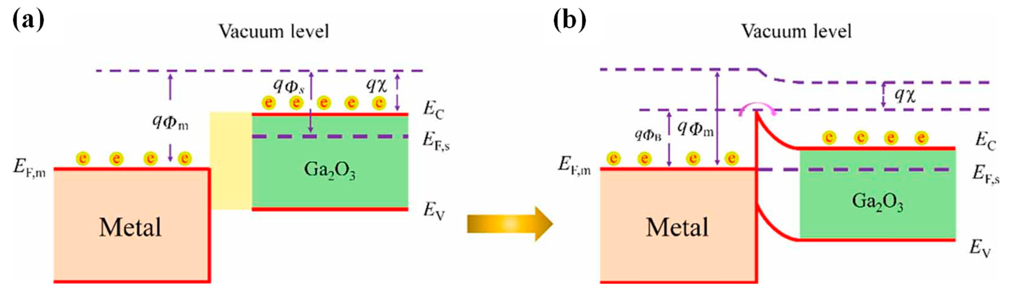
Figure 4.
Device schematic of vertical β-Ga2O3 SBDs on (a) β-Ga2O3 substrate and (b) with β-Ga2O3 epi-layer on β-Ga2O3 substrate.
Figure 4.
Device schematic of vertical β-Ga2O3 SBDs on (a) β-Ga2O3 substrate and (b) with β-Ga2O3 epi-layer on β-Ga2O3 substrate.

Figure 5.
Device schematic of β-Ga2O3 FP-SBDs with (a) SiO2 field plate [144]; (b) SiO2/SiNx bilayer field plate [148]; (c) small-angle beveled field plate [149]; (d) stair field plate [150].

Figure 6.
Device schematic of β-Ga2O3 SBDs with edge termination structure.

Figure 8.
Device schematic of mesa termination structure β-Ga2O3 SBDs with (a) 4 µm deep mesa [195]; (b) PtOx Schottky electrode [196]; (c) beveled F plasma-treated (BFPT) structure (right) [197].

Figure 9.
Device schematic of (a) FP-NB SBD and (b) SEM cross-section image; (c) PB SBD and (d) SEM cross-section image [199]; (e) β-Ga2O3 BFP and SABFP SBDs [200].
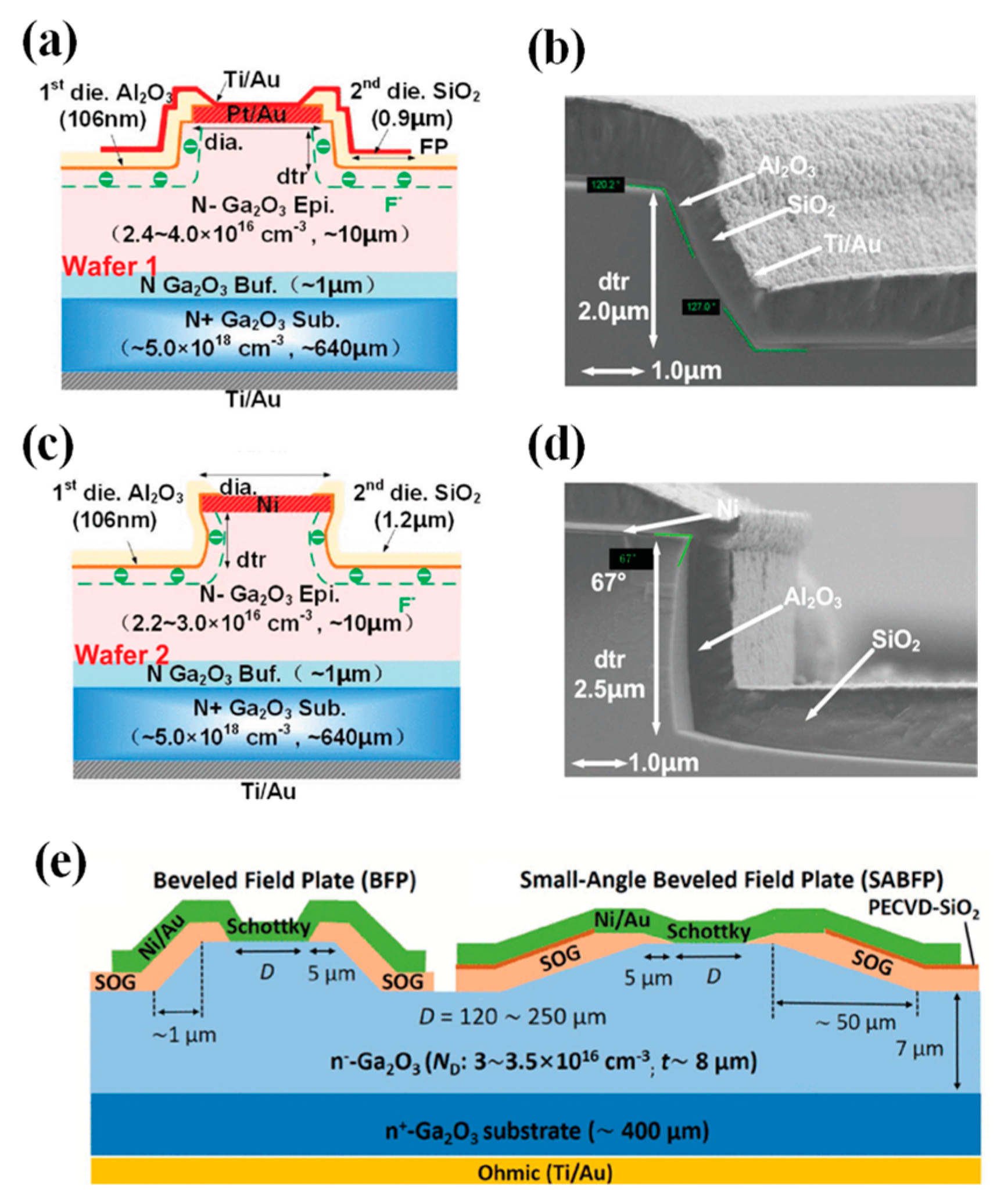
Figure 11.
Device schematic of NiO/β-Ga2O3 HJDs with (a) SiNx/SiO2 bilayer field plate structure [228]; (b) small-angle BFP [229]; (c) Mg ion implantation terminals and SiO2 field plate structure [39].
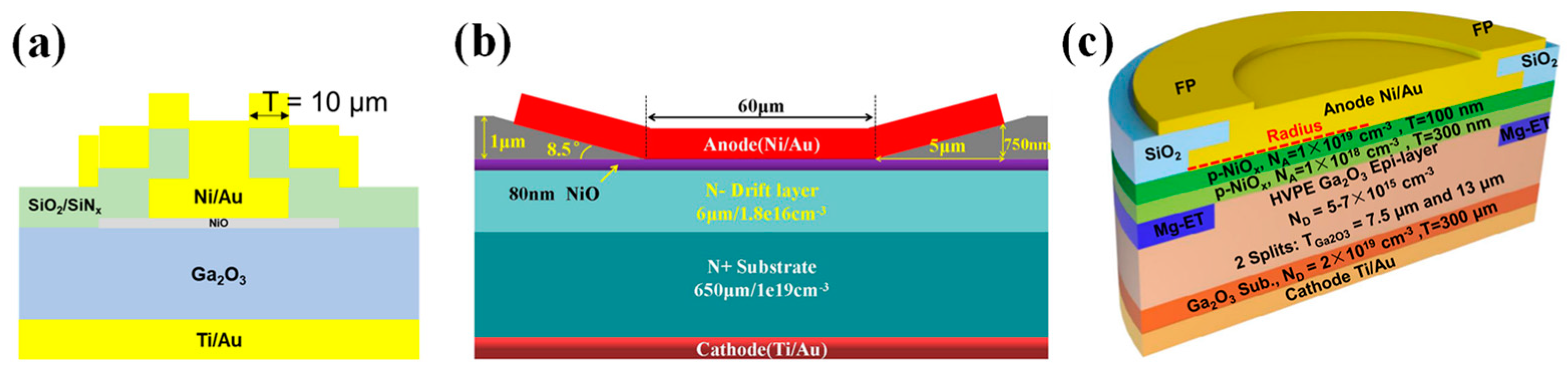
Figure 12.
Device schematic of (a) β-Ga2O3 HJBS diodes with thermally oxidized p-NiO [235]; (b) β-Ga2O3 HJBS diodes with sputter-deposited p-NiO [236]; (c) NiO/β-Ga2O3 HJDs, HJBS-2 µm diodes terminated with p-NiO FLRs, Ni/β-Ga2O3 SBDs, and Ni/β-Ga2O3 SBDs terminated with p-NiO FLRs [237]; (d) β-Ga2O3 HJBS diodes with SiO2 field plate [238]; (e) β-Ga2O3 HJBS diodes with beveled field plate structure (left) and without beveled field plate (right) [239].
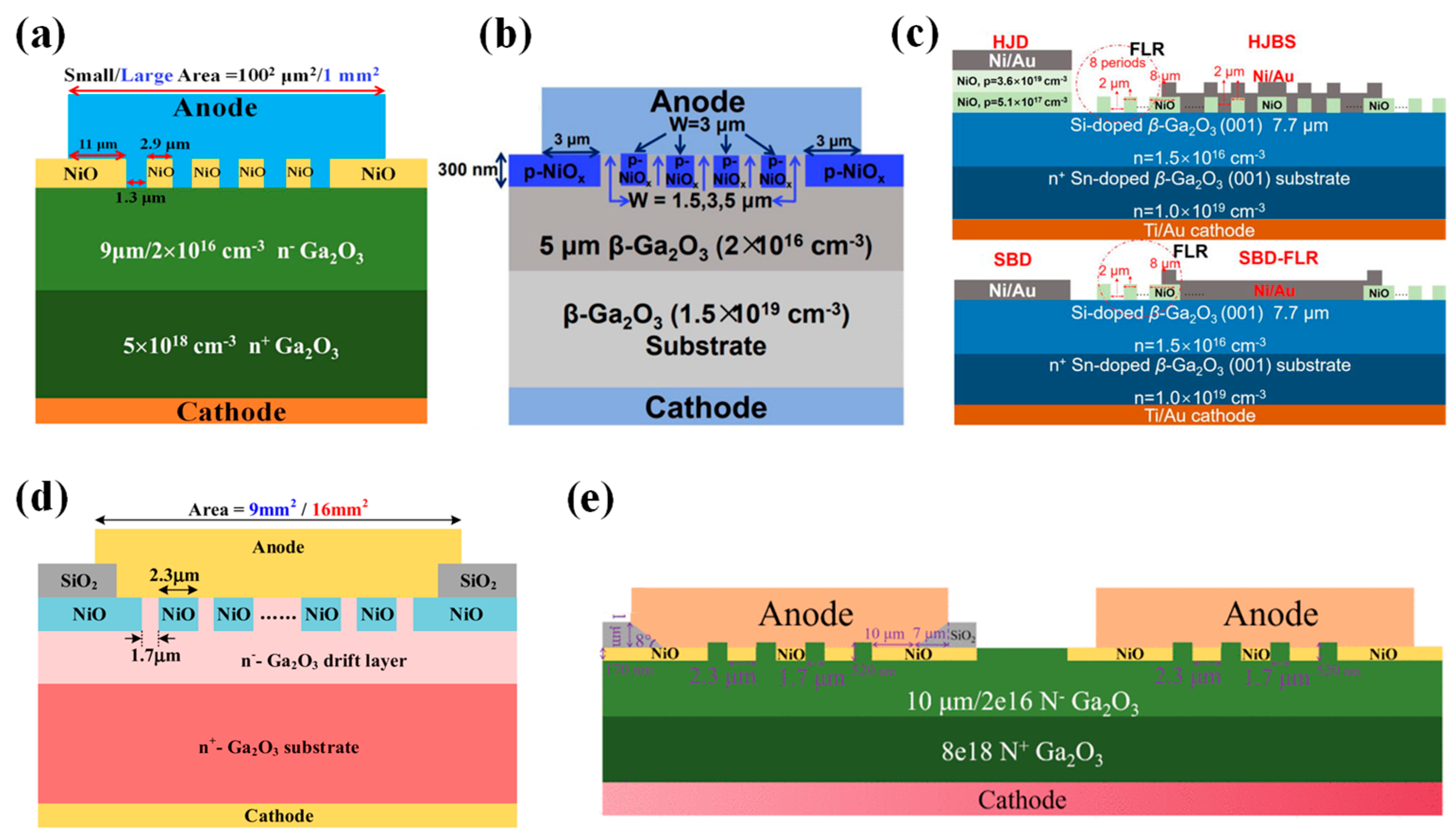
Figure 13.
(a) Schematic cross-sectional diagram of NiOx/β-Ga2O3 HJBS diodes; (b) schematic (top views) of anode layout of stripe HJBS diodes and (c) honeycomb HJBS diodes. (The green regions are p-NiOx and the white regions are Ga2O3.) [240].
Figure 13.
(a) Schematic cross-sectional diagram of NiOx/β-Ga2O3 HJBS diodes; (b) schematic (top views) of anode layout of stripe HJBS diodes and (c) honeycomb HJBS diodes. (The green regions are p-NiOx and the white regions are Ga2O3.) [240].

Figure 14.
Device schematic of (a) β-Ga2O3 SBDs with p-NiO JTE [242]; (b) β-Ga2O3 SBDs with NiO stair-shaped JTE [243]; (c) NiO/β-Ga2O3 HJDs with NiO stair-shaped JTE [244]; (d) β-Ga2O3 SBDs with p-NiOx edge termination extension structure [245]; (e) β-Ga2O3 SBD with edge termination extension and field plate structure [246]; (f) β-Ga2O3 SJ-SBDs [247].

Figure 15.
Device schematic of (a) lateral β-Ga2O3 SBDs on sapphire substrate and top-view microscopy image [248]; (b) lateral β-Ga2O3 SBDs with field plate structure and top-view microscopy image [249]; (c) lateral β-Ga2O3 SBDs with bilayer field plate [38]; (d) β-Ga2O3 lateral super junction SBDs with BaTiO3 dielectric [250]; (e) β-Ga2O3 field-effect rectifier with a p-NiOx gate [251]; (f) lateral β-Ga2O3 RESURF SBDs [37].
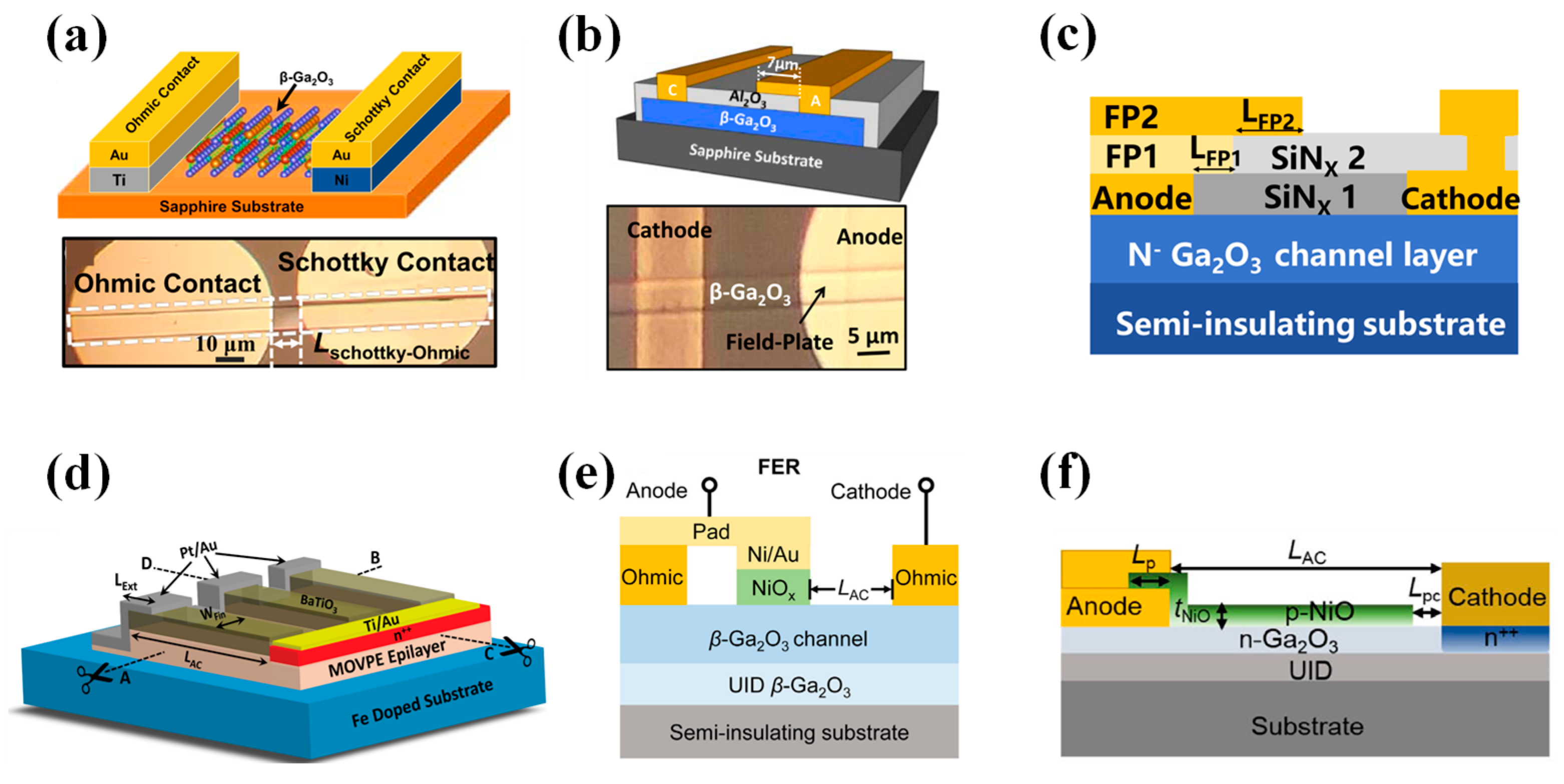
Figure 16.
Schematic of β-Ga2O3 SBDs with (a) bottom-side-cooling package and (b) double-side-cooling flip-chip package [269]; (c) schematic structure of thin-body β-Ga2O3 SBD with flip-chip packaging [271].
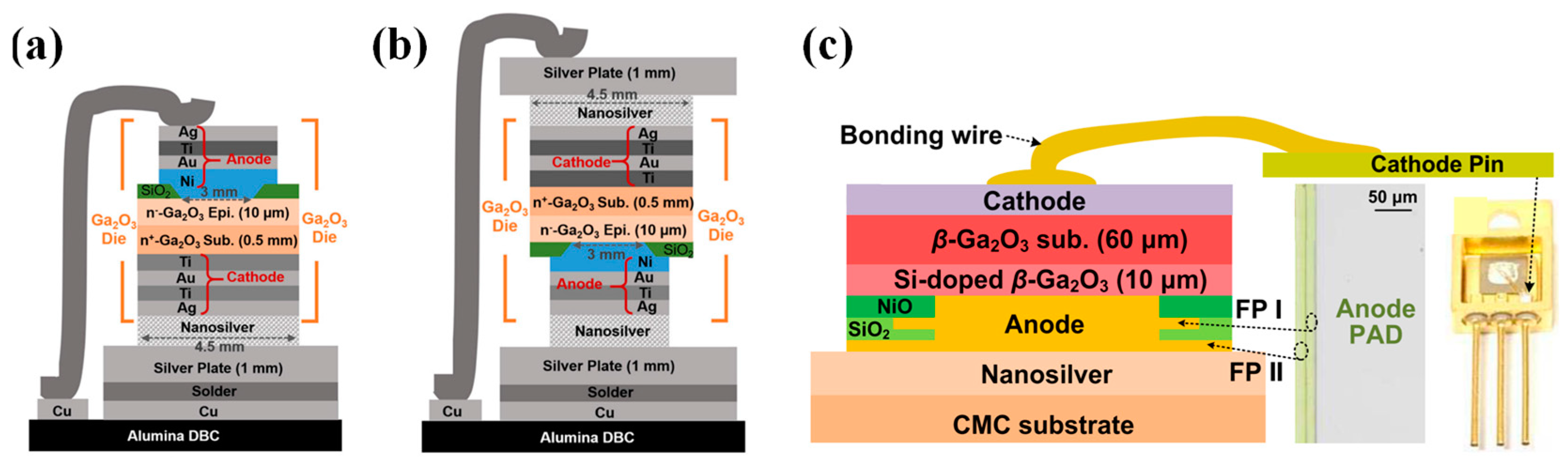
Figure 17.
(a) Schematic of the DC-DC converter based on the β-Ga2O3 SBDs [274]; (b) circuit of the four-stage HW series CW voltage multiplier circuit with β-Ga2O3 HJBS diodes [239].
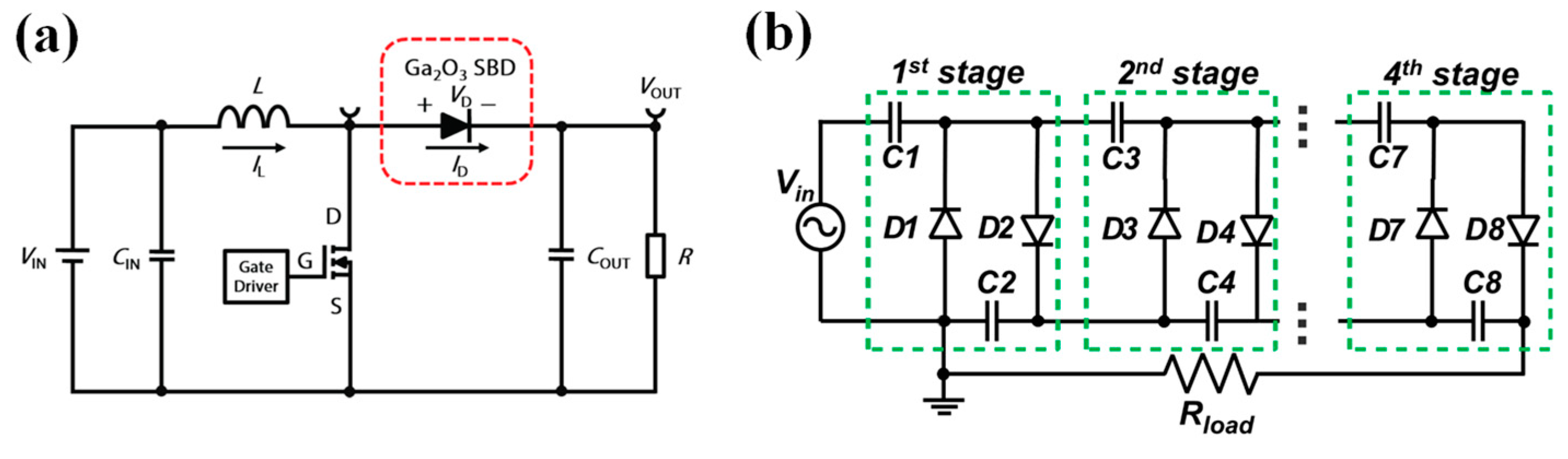

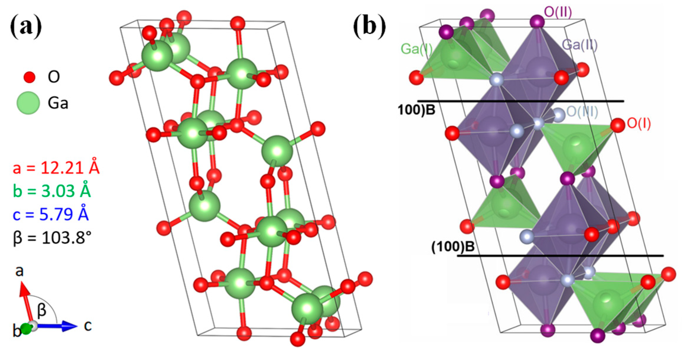
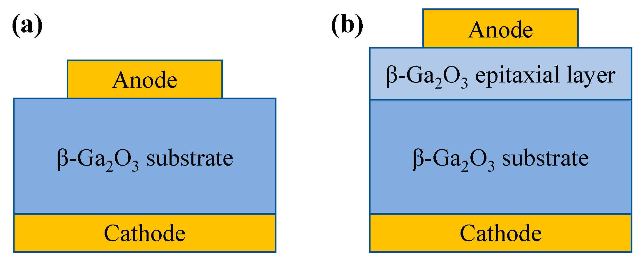
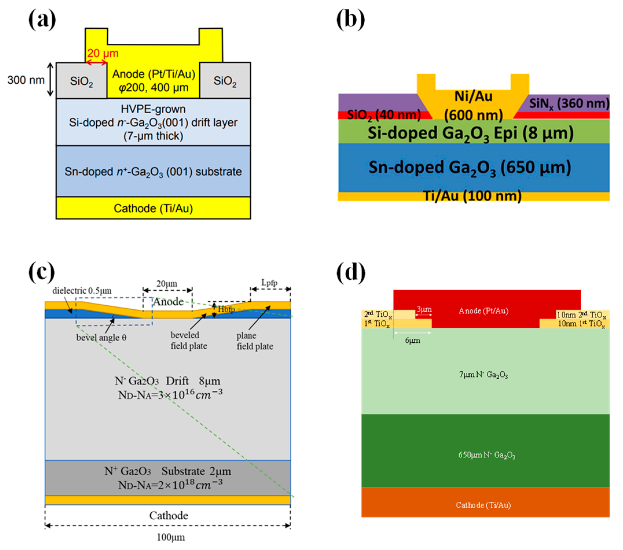
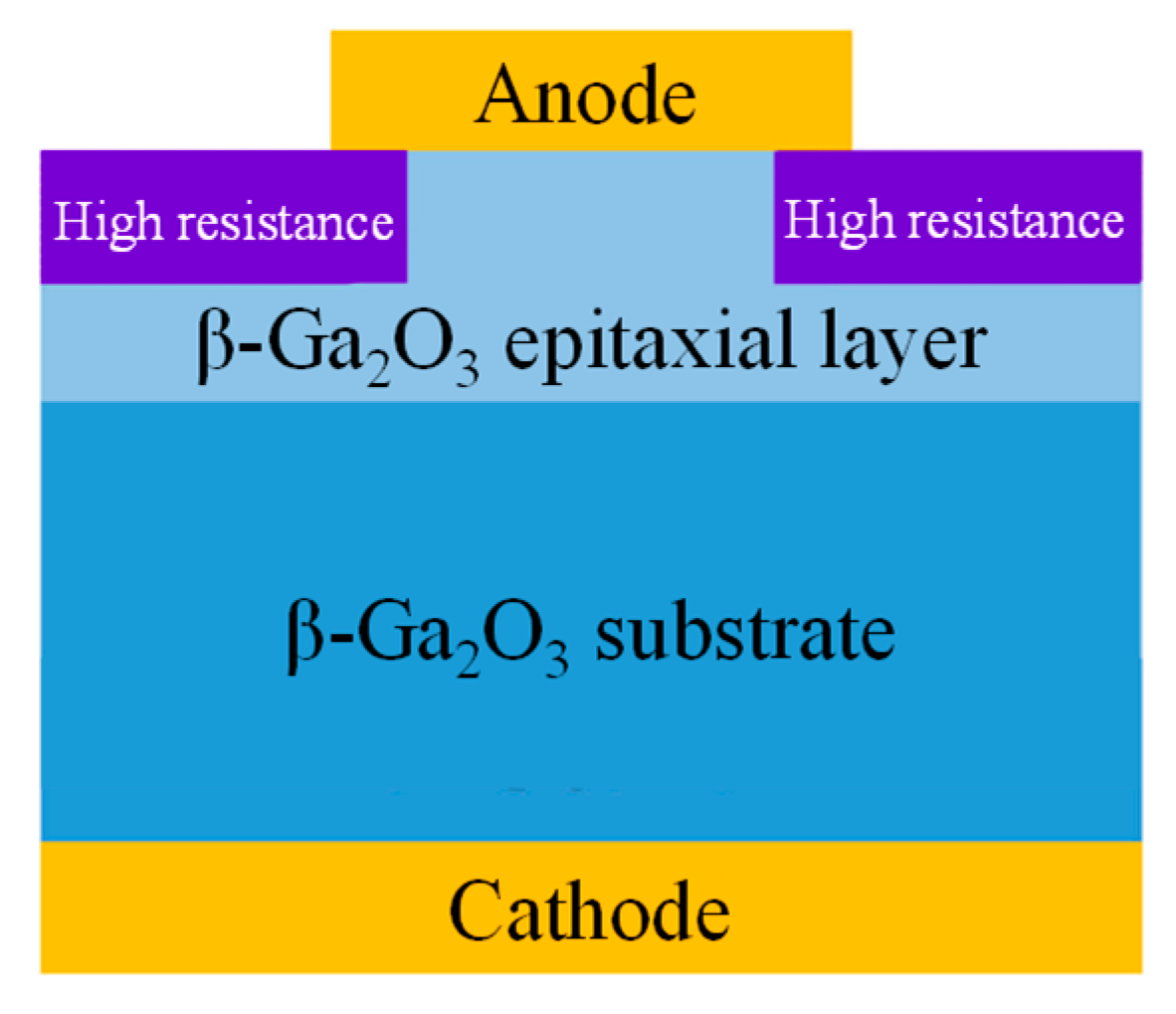
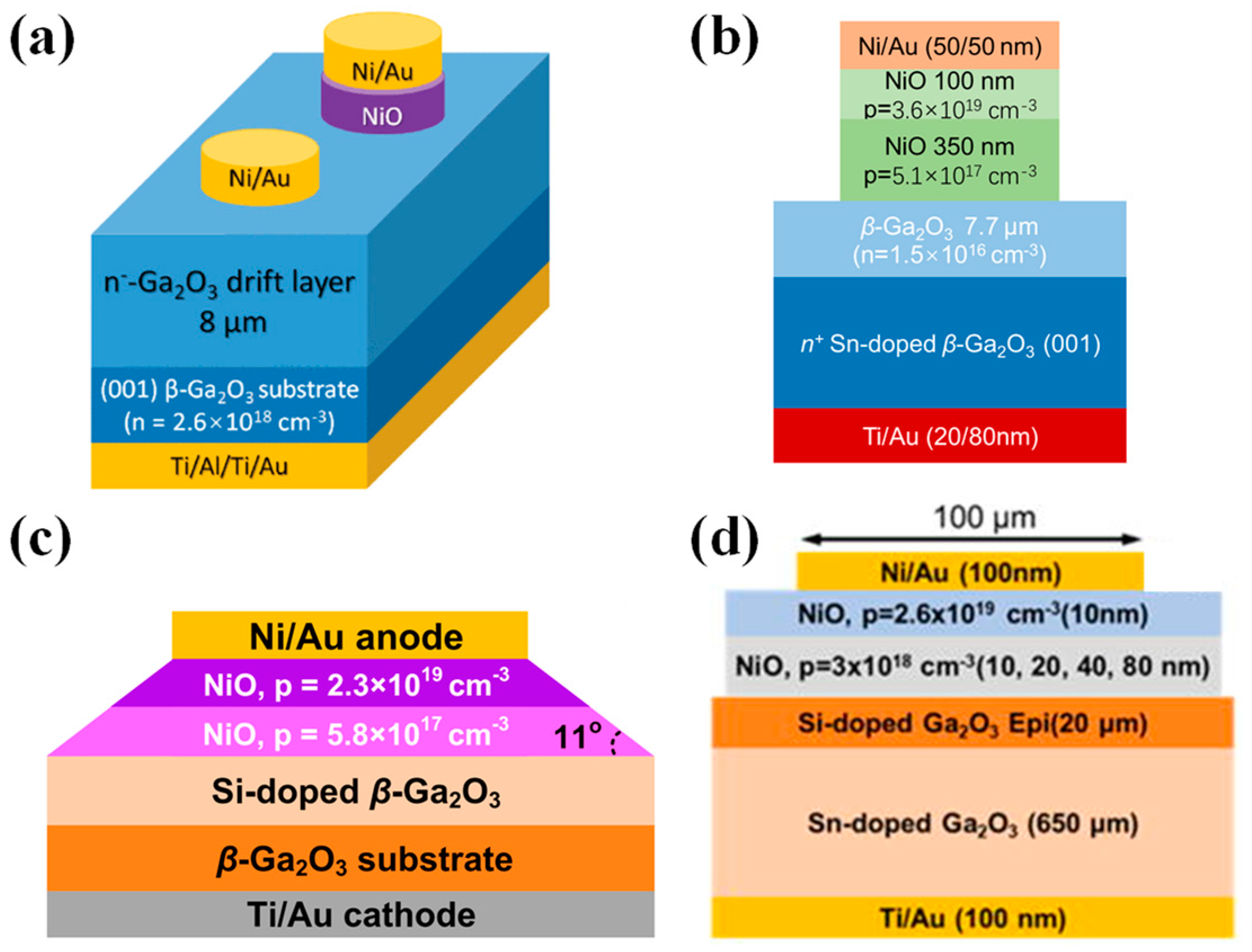
Table 1.
Comparative analysis of performance parameters of different power semiconductor materials [19,96].
| Material Parameters | Si | GaAs | 4H-SiC | GaN | β-Ga2O3 | Diamond |
|---|---|---|---|---|---|---|
| Bandgap, Eg (eV) | 1.1 | 1.43 | 3.25 | 3.4 | 4.7–4.9 | 5.5 |
| Electron mobility, µ (cm2/V·s) | 1480 | 8400 | 1000 | 1250 | 300 | 2000 |
| Breakdown field, Ec (MV/cm) | 0.3 | 0.4 | 2.5 | 3.3 | 8 | 10 |
| Saturation velocity, vs (107 cm/s) | 1 | 1.2 | 2 | 2.5 | 1.8–2 | 1 |
| Dielectric constant, ε | 11.8 | 12.9 | 9.7 | 9 | 10 | 5.5 |
| Thermal conductivity, λ (W/cm·K) | 1.5 | 0.5 | 4.9 | 2.3 | 0.1–0.3 | 20 |
| Baliga, εµEc3 | 1 | 14.7 | 317 | 846 | 3444 | 24,660 |
Table 2.
Comparison of electrical performances for different-structure β-Ga2O3 SBDs.
| Device Structure | Anode Area | Von (V) | IF | Ron | BV | PFOM (GW/cm2) | References |
|---|---|---|---|---|---|---|---|
| (mΩ·cm2) | (kV) | ||||||
| w/o unreliable surface | Φ100 µm | — | — | 2.25 | 1.72 | 1.32 | [138] |
| BTO FP | Φ50–300 µm | — | — | 6.9–8.7 | 2.1 | 0.51–0.64 | [157] |
| Mg ion implantation ET | Φ180 µm | — | 200 A/cm2@2 V | 5.1 | 1.55 | 0.47 | [165] |
| Oxygen-annealing ET | Φ110 µm | — | — | 4.1 | 1.8 | 0.78 | [172] |
| SiO2 ET | Φ180 µm | 1.45 | 400 A/cm2@3 V | 3.4 | 6 | 10.6 | [173] |
| Trench with FP | 100 × 150 µm2 | — | — | 8.8 (pulsed) | 2.89 | 0.95 (pulsed) | [188] |
| Trench with BTO dielectric | 200 × 200 µm2 | — | — | 6.8 | >3 | >1.32 | [190] |
| 1 × 1 mm2 | 0.9 | 3.7 A@5 V (pulsed) | 7.1 | 1.8 | 0.46 | ||
| 2 × 2 mm2 | — | 15 A@5 V (pulsed) | 10.8 | 1.4 | 0.18 | ||
| MT with PtOx | Φ100 µm | 1.45 | — | 7.33 | 2.74 | 1.02 | [196] |
| MT with PBT | Φ100 µm | 1.48 | — | 3.6 | 1.71 | 0.8 | [199] |
| AHJD | Φ100 µm | 1.72 | — | 2.5 | 2.66 | 2.83 | [218] |
| Beveled-mesa HJD | 1 × 1 mm2 | 1.82 | 20 A@ < 12 V | 1.9 | 1.95 | 2 | [219] |
| Double-layered NiO HJD | Φ100 µm | 1.9–2.1 | >100 A/cm2@3 V | 7.9 | 8.9 | 10.2 | [226] |
| 1 × 1 mm2 | — | 4.1 A@10 V | 1.8 | >4 | 9 | ||
| HJD with SiOx/SiOx FP | 1 × 1 mm2 | ~2 | 1 A@3 V | 5.4 | 7 | 9.2 | [228] |
| HJD with BFP | Φ60 µm | 1.6 | — | 1.12 | 2.41 | 5.18 | [229] |
| HJD with FP and ET | Φ150 µm | 1.8 | ~400 A/cm2@5 V | 5.24 | 8.32 | 13.2 | [39] |
| HJD with JTE | Φ100 µm | — | — | 3.9 | >3.2 | 2.5–2.7 | [244] |
| Vertical SJ | — | 1 | — | 0.7 | 2 | 5.71 | [247] |
| Lateral with dual FP and PAAT | LAC=90 µm | 1.02 | 7.43 mA/mm@5 V | 485 | >10 | >0.21 | [38] |
| Lateral SJ with BTO | LAC/WFin = 5 µm/2 µm | — | — | 1.65 | 1.49 | 1.34 | [250] |
| Lateral with charge balance | LAC>30 µm | 1 | — | 270 | >10 | >0.37 | [37] |
Disclaimer/Publisher’s Note: The statements, opinions and data contained in all publications are solely those of the individual author(s) and contributor(s) and not of MDPI and/or the editor(s). MDPI and/or the editor(s) disclaim responsibility for any injury to people or property resulting from any ideas, methods, instructions or products referred to in the content. |
© 2024 by the authors. Licensee MDPI, Basel, Switzerland. This article is an open access article distributed under the terms and conditions of the Creative Commons Attribution (CC BY) license (https://creativecommons.org/licenses/by/4.0/).
Share and Cite
MDPI and ACS Style
He, Y.; Zhao, F.; Huang, B.; Zhang, T.; Zhu, H. A Review of β-Ga2O3 Power Diodes. Materials 2024, 17, 1870. https://doi.org/10.3390/ma17081870
AMA Style
He Y, Zhao F, Huang B, Zhang T, Zhu H. A Review of β-Ga2O3 Power Diodes. Materials. 2024; 17(8):1870. https://doi.org/10.3390/ma17081870
Chicago/Turabian StyleHe, Yongjie, Feiyang Zhao, Bin Huang, Tianyi Zhang, and Hao Zhu. 2024. "A Review of β-Ga2O3 Power Diodes" Materials 17, no. 8: 1870. https://doi.org/10.3390/ma17081870
Note that from the first issue of 2016, this journal uses article numbers instead of page numbers. See further details here.