
Fabrication of Cu2Sn1-xGexS3 Thin-Film Solar Cells via Sulfurization of Cu2GeS3/Cu2SnS3 Stacked Precursors

National Institute of Technology (KOSEN), Nagaoka College, Nagaoka 940-8532, Japan
*
Author to whom correspondence should be addressed.
Materials 2024, 17(8), 1886; https://doi.org/10.3390/ma17081886
Submission received: 4 August 2023
/
Revised: 3 April 2024
/
Accepted: 9 April 2024
/
Published: 19 April 2024
(This article belongs to the Special Issue Science and Technology of Advanced Materials Applied to Society: Including Collections from the Latest Papers of KRIS 2023)
Abstract
:Cu2Sn1-xGexS3 (CTGS) is a compound composed of relatively abundant elements in the crust of the earth. The band gap of CTGS can be tuned by substituting elements at the Sn and Ge sites, making it an attractive material for low-environmental-impact solar cells. In this study, CTGS thin films were fabricated with a controlled [Ge]/([Ge] + [Sn]) composition ratio (x) by combining the co-evaporation method and sulfurization in an infrared furnace. Furthermore, the effect of Na on the CTGS and changes in the solar cell properties were investigated by stacking and sulfurizing NaF on the precursor fabricated using the co-evaporation method. As a result, CTGS with varying x was successfully fabricated by varying the deposition time of the Cu2GeS3 layer using co-evaporation. Additionally, CTGS prepared by doping with Na showed enlarged CTGS crystals compared to Na-free CTGS. The fabricated CTGS solar cells achieved a power conversion efficiency of more than 4.5% after doping with Na.
1. Introduction
Cu2Sn1-xGexS3 (CTGS) is a solid solution of Cu2SnS3 (CTS) and Cu2GeS3 (CGS) and is a promising candidate material for next-generation solar cells. CTS is a p-type semiconductor with a band gap energy of approximately 0.9 eV and a high optical absorption coefficient of more than 104 cm–1 in the visible to the near-infrared region [1]. CGS has been reportedly fabricated in bulk crystals [2], and its band gap energy is estimated to be approximately 1.5 eV [3]. By varying the Ge composition ratio (x), the band gap of CTGS can be tuned almost linearly between 0.9 and 1.5 eV in bulk crystals [4,5,6] and nanoparticles [7], making it suitable as a light-absorbing layer in solar cells. Furthermore, the constituent elements are inexpensive and non-toxic compared to the leading compounds in solar cells, such as Cu(In,Ga)(S,Se)2, CdTe, and Cu2ZnSn(S,Se)4. In addition, excellent atmospheric stability has been reported in CTS-based solar cells [8]. Therefore, solar cells composed of CTGS, which is similar to CTS, are expected to have advantages over perovskite solar cells [9,10], which have been the focus of recent attention, in that they do not contain Pb and are more stable in air. Consequently, various compositions and fabrication processes have been reported for CTGS thin-film solar cells, including CTS cells corresponding to x = 0 and CGS thin-film solar cells corresponding to x = 1. As shown in Table 1 [11,12,13,14,15,16,17,18,19,20], a type of CTGS with x = 0 (i.e., CTS), achieved a power conversion efficiency (PCE) of more than 5% [11,12]. PCEs exceeding 5% have also been reported in CTGS solar cells fabricated by alloying Ge with CTS in thin films fabricated by the sulfurization of Ge/Cu–SnS2 precursors with S and SnS2 [14] and in thin films obtained by the sulfurization of Cu–Sn metal precursors with S and GeS2 vapor [15,16]. In particular, the highest reported PCE of 6.7% was obtained for CTGS-based solar cells using a gradient band gap structure formed by varying x of CTGS in the depth direction of the thin film [16]. Similarly, we previously reported several CTGS thin films fabricated using the co-deposition method, including CTS thin-film solar cells with x = 0 [21,22,23,24,25]. However, none of these CTGS efficiencies are sufficient for practical use, as the PCE does not reach above 20% as in practical Cu(In,Ga)(S,Se)2 and CdTe solar cells [26,27]. In this work, to improve the efficiency of CTGS solar cells, a co-deposition method using a Knudsen cell was employed, which allows precise control of the deposition source temperature. This method can control a wide range of complex processes and compositions, such as the three-stage process (deposition rate vs. time control) used for CIGS film formation [28]. Thus, the advantages include the ease of switching deposition conditions, such as depositing a CTS layer immediately after the CGS layer, and the study of appropriate stacking conditions. Using this co-evaporation method, we prepared a stacking precursor of the Cu2GeS3/Cu2SnS3 structure and fabricated dense, flat, high-quality CTGS thin films by sulfurizing the obtained precursor films. We attempted to fabricate CTGS thin films using CGS/CTS stacking precursors as a method different from that employed in the previous study, in which single-layer precursor thin films were prepared by the co-deposition of CTGS thin films. Furthermore, CTS thin-film solar cells with Na doping by the sulfurization of NaF-deposited precursor thin films have been reported to exhibit improved solar cell characteristics [11,12]. Therefore, we also investigated the effect of Na on CTGS by combining precursor fabrication using the co-evaporation method and sulfurization with NaF stacking and evaluated the resulting changes in the CTGS solar cell’s properties.
2. Materials and Methods
The following materials were procured: Mo disc (99.95%, 3 mm thick, Fruuchi Chemical Corporation, Tokyo, Japan), Cu shot (99.9999%, Fruuchi Chemical Corporation, Japan), Sn shot (99.9999%, Fruuchi Chemical Corporation, Japan), Ge shot (99.999%, Fruuchi Chemical Corporation, Japan), sodium fluoride (NaF, 99%, Nacalai tesque, Inc., Kyoto, Japan), S chunk (99.9999%, Fruuchi Chemical Corporation, Japan), cadmium iodide (CdI2, 99%, FUJIFILM Wako Pure Chemical Corporation, Osaka, Japan), Thiourea (CS(NH2)2, 98%, Nacalai tesque, INC., Kyoto, Japan), ammonia water (NH3, 28 wt%, Fujifilm Wako Pure Chemical Corporation, Osaka, Japan), ZnO: Al sputter target (Al2O3, 2 wt%, 3 mm thick, 99.99%, Fruuchi Chemical Corporation, Japan), and Al (99.99%, Niraco Corporation, Tokyo, Japan).
Figure 1 shows a schematic of the CTGS solar cell fabrication process. The Mo back-contact film is formed on an alkali-free glass substrate EAGLE-XG using DC sputtering. The sputtering conditions are as follows: deposition time, 25 min; applied current, 1.0 A; process pressure, 0.4 Pa; and Ar flow, 20 sccm. CGS and CTS thin films were deposited using a Cu, Ge, Sn, and S co-deposition system (EIKO Co., Tokyo, Japan). The S flux was activated by thermal cracking at 800 °C with S evaporated at 150 °C using the needle valve cracker cell as the S source. The Cu, Sn, and Ge K-cells and the valved cell for S were arranged such that the distance between the aperture position of the cells and the center of the substrate was 215 mm. The CGS layer was prepared by evaporating Cu and Ge with S flux on a Mo-coated substrate under a growth chamber pressure of 10−4 Pa. The evaporation rates for Cu and Ge were 0.22 and 0.35 Å/s, respectively. The deposition time tCGS of the CGS layer was 0.0–1.5 h. tCGS = 0.0 means that the film is not deposited with CGS. Thus, it is a sample fabricated by depositing only the CTS layer. Subsequently, a CTS layer was prepared by depositing Cu and Sn in S flux on the CGS layer. The Sn evaporation rate was 0.35 Å/s. The evaporation time of the CTS layer was varied based on the preceding CGS evaporation time such that the total time for both layers was 3 h. The composition ratio of the fabricated CGS/CTS stacked precursor was measured using wavelength-dispersive X-ray fluorescence (XRF) analysis (ZSX Primus IV, Rigaku, Tokyo, Japan). The NaF layer was deposited on the precursor via thermal evaporation using 10 mg NaF as an evaporation source. Similarly, for comparison, precursors without NaF deposition were prepared. The precursor was placed in a carbon susceptor containing 100 mg of S and sulfurized in an infrared furnace. The sulfurization procedure was implemented by increasing the temperature to 570 °C at a rate of 2 °C/s for 10 min, which was followed by cooling at room temperature. To remove the water-soluble impurities from the sulfurized CTGS thin film, it was immersed in 50 mL of deionized water for 30 min. The composition of these CTGS films was characterized using XRF. The crystal structure was analyzed by performing X-ray diffraction (XRD; MiniFlex, Rigaku, Japan). The surface and cross-sectional morphologies of these thin films were observed using scanning electron microscopy (SEM) (JSM-6060LV, JEOL, Tokyo, Japan). An n-type CdS layer was deposited on the obtained CTGS thin film via chemical bath deposition, and n-type ZnO: Al was prepared via RF sputtering. The reaction conditions for the chemical bath deposition method were previously reported [23]. Here, the CdS buffer layer was an n-type semiconductor with a thickness of approximately 90 nm and was used to form a p-n junction with proper band alignment with CTGS, which was a p-type semiconductor. The transparent conducting oxide layer, ZnO: Al, transmitted light to the CTGS/CdS layer and conducted the photogenerated electrons to the top Al electrode. Finally, solar cells with an EAGLE-XG/Mo/CTGS/CdS/ZnO:Al/Al structure were fabricated by evaporating Al top contacts, and the current density–voltage characteristics were measured using a Xe lamp type solar simulator (SX-UI 500XQ) under irradiation (AM 1.5G and 100 mW/cm2).
3. Results and Discussion
Table 2 shows the composition ratio x = [Ge]/([Ge] + [Sn]) (hereafter denoted as x) values evaluated via XRF analysis using the CGS/CTS stacked precursor and the thin films obtained via sulfurization. In all thin films, the [Cu]/([Ge] + [Sn]) composition ratio was Cu-poor below the stoichiometric composition ratio of 2.0.
In CTGS, Cu-rich compositions are not suitable for solar cell applications because they induce the formation of short-circuiting CuS [1,29]. The [Cu]/([Ge] + [Sn]) composition ratios obtained in this study are all Cu-poor compositions suitable for solar cell applications. The [Ge]/([Ge] + [Sn]) x ratio increased with increasing tCGS. However, x in the sulfurized thin film was slightly lower than in the precursor in both cases. Figure 2 shows the behavior of x before and after sulfurization.
If the composition of the precursor thin film before sulfurization and that of the CTGS thin film after sulfurization are the same (i.e., unchanged), then the plot of the marker overlaps the dotted line in Figure 2. However, in the presented results, the marker is plotted below the dotted line because the composition before sulfurization is different from that after sulfurization. This behavior indicates that the [Ge]/([Ge] + [Sn]) composition ratio has decreased due to sulfurization. The Na-doped CTGS showed a remarkable decrease in x after sulfurization compared to the Na-free CTGS. This result suggests that sulfurization may have re-evaporated Ge-containing compounds. GeS with a higher vapor pressure than SnS is a candidate compound that likely causes re-evaporation [30,31]. Conversely, in the present study, S desorption was avoided by annealing with S lumps. As evidenced, the composition ratio [S]/([Cu] + [Ge] + [Sn]) after sulfurization was greater than the stoichiometric ratio of 1.0 in all thin films. The x = 0.00 thin film of Na-free CTGS could not be measured because it was largely peeled off during immersion in deionized water.
Figure 3 shows the XRD results of the Na-doped and Na-free CTGS thin films. Figure 3a depicts the XRD spectra of Na-doped CTGS, where a peak near the diffraction peak of CTS with a monoclinic structure (ICDD Powder Diffraction File (PDF) #01-070-6338) is observed. Peaks attributable to monoclinic CTS are observed for the sample with x = 0.00, whereas peaks at x = 0.27 and 0.41 are observed at an angle slightly higher than in CTS and lower than in CGS (PDF#01-088-0827). This result is suggested to be due to a decrease in the lattice parameter caused by the substitution of Ge for a part of Sn in CTS, indicating the formation of CTGS. A small peak is evident around 36.4° for the x = 0.27 and 0.44 samples, but no corresponding peak is observed for the x = 0 sample, suggesting the possibility of an impurity phase. Figure 3b shows the XRD spectra of the Na-free CTGS. The peak at x = 0.00 is attributable to CTS with a monoclinic structure. For the samples at x = 0.32 and 0.44, diffraction peaks are observed at angles slightly higher than that of CTS and lower than that of CGS (PDF#01-088-0827). This result is suggested to be due to a decrease in the lattice constant due to the substitution of Ge for some of the Sn in CTS by the formation of the solid solution CTGS. Furthermore, these peaks for the Na-free CTGS are broader than those in the Na-doped sample, suggesting that the [Ge]/([Ge] + [Sn]) composition ratio x in the thin film is not unity in the Na-free sample compared to the Na-doped films and that the composition distribution in the film is larger. In the Na-free CTGS thin film at x = 0.00, a peak is found around 34° that is not observed in the Na-doped sample. This peak near 34° is attributed to SnS2 (PDF #01-084-9295), which can be ascribed to the Cu-poor composition of the precursor. In addition, unattributed peaks were observed at 36° for x = 0.32 and 0.44, which is similar to the Na-doped sample.
Figure 4 shows the magnified XRD spectra near the (200) planes of CTS and CGS in the monoclinic structure. Figure 4a depicts the XRD spectra of the Na-doped CTGS in which the peak shifts to a higher angle as x increases. This behavior implies that the lattice of CTGS shrinks as the amount of Ge-substituted Sn sites in CTS increases. Figure 4b presents the magnified XRD spectrum of the Na-free CTGS. The diffraction peak of the thin film with x = 0 coincides with the peak of CTS in the monoclinic structure. However, for x = 0.32 and 0.44 thin films, broad peaks are observed at angles between those expected for CTS and CGS. This finding indicates that the CTGS thin films do not have a single composition and contain regions of different Ge composition ratios. The peaks of the Na-doped sample are sharper than those of the Na-free sample, indicating that sulfurization with Na doping promotes a single composition of Ge in CTGS. The diffraction angle of the maximum diffraction peak intensity is slightly higher at x = 0.44 than at x = 0.32. As with the Na-doped sample, a decrease in the lattice constant with the increasing Ge composition ratio in the sample is suggested.
Figure 5 presents the diffraction angles of the maximum-intensity peaks, corresponding to the (200) plane of CTGS, as functions of the Ge composition (x) values. In the case of the Na-free CTGS sample, the diffraction peak of the (200) plane detected at x = 0.44 is broad, and the peak top is not clear; thus, an error bar has been included. The peak angles for Na-doped CTGS and Na-free CTGS show a trend of linear shift with increasing x, which is consistent with Vegard’s law. Therefore, the Ge composition can be controlled by sulfurization of the CGS/CTS stacking precursor with varying tCGS with or without Na.
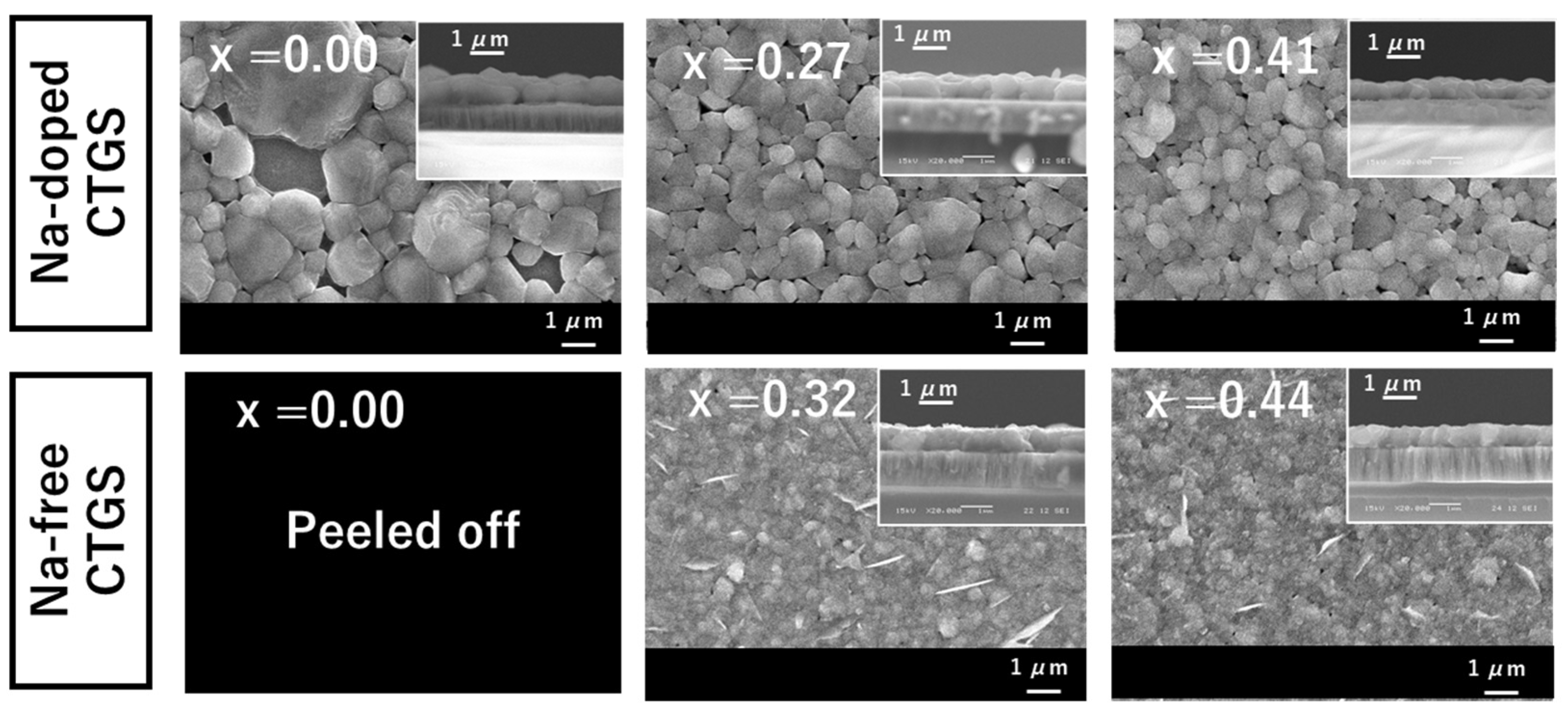
Figure 6 shows the surface and cross-sectional SEM images of the fabricated CTGS thin films after sulfurization. The surfaces of the Na-free CTGS films exhibit fine crystal grains. Thin plate-like compounds are observed on the surfaces of the CTGS thin films with x-values of 0.32 and 0.44. The observation of similar plate-like morphology has been reported in SnS and SnS2 deposition [32,33]. After sulfurization, the concentration of Cu in Na-free CTGS was lower than that in Na-doped CTGS, and SnS2 was detected at x = 0.00, as shown Figure 3b. These results and the similar morphologies suggest that the plate-like segregation observed on the surfaces of the samples at x = 0.32 and 0.44 may be assigned to a small amount of SnS and/or SnS2 that cannot be detected by XRD. Significant crystal growth is observed in the Na-doped CTGS films compared to that in the Na-free CTGS films. The Na-doped CTGS thin film with x = 0.00 shows higher crystal growth, which is consistent with previous reports of CTS [11,23,34]. Similarly, the growth of CTGS crystals is enhanced in the thin films with x-values of 0.27 and 0.41, suggesting that Na plays a positive role in promoting the growth of CTGS crystals. For CTS thin films, the addition of Na has been reported to enlarge the grains of the thin film significantly, and with the help of NaF, a monoclinic CTS structure has reportedly been formed at a lower substrate temperature than without Na addition [34]. Similarly, the addition of Na to the CTGS thin film promotes the growth of crystal grains in the CTGS film during the heat-treatment process, and the CTS and CGS microcrystals in the CGS/CTS stacked precursor film form CTGS. In addition, the grain boundaries reduce as the crystals grow into large crystal grains with monoclinic structures. In this case, the different phases (SnS2, etc.) are consumed as raw materials for the growth of large crystals grain or re-evaporate owing to heat treatment. However, the detailed mechanisms underlying the growth of Na-added CTS and CTGS thin-film crystals remain obscure, and further investigations are required. The voids observed in the Na-doped CTGS thin films may be attributed to the re-evaporation of compounds with high vapor pressures, such as SnS and GeS.
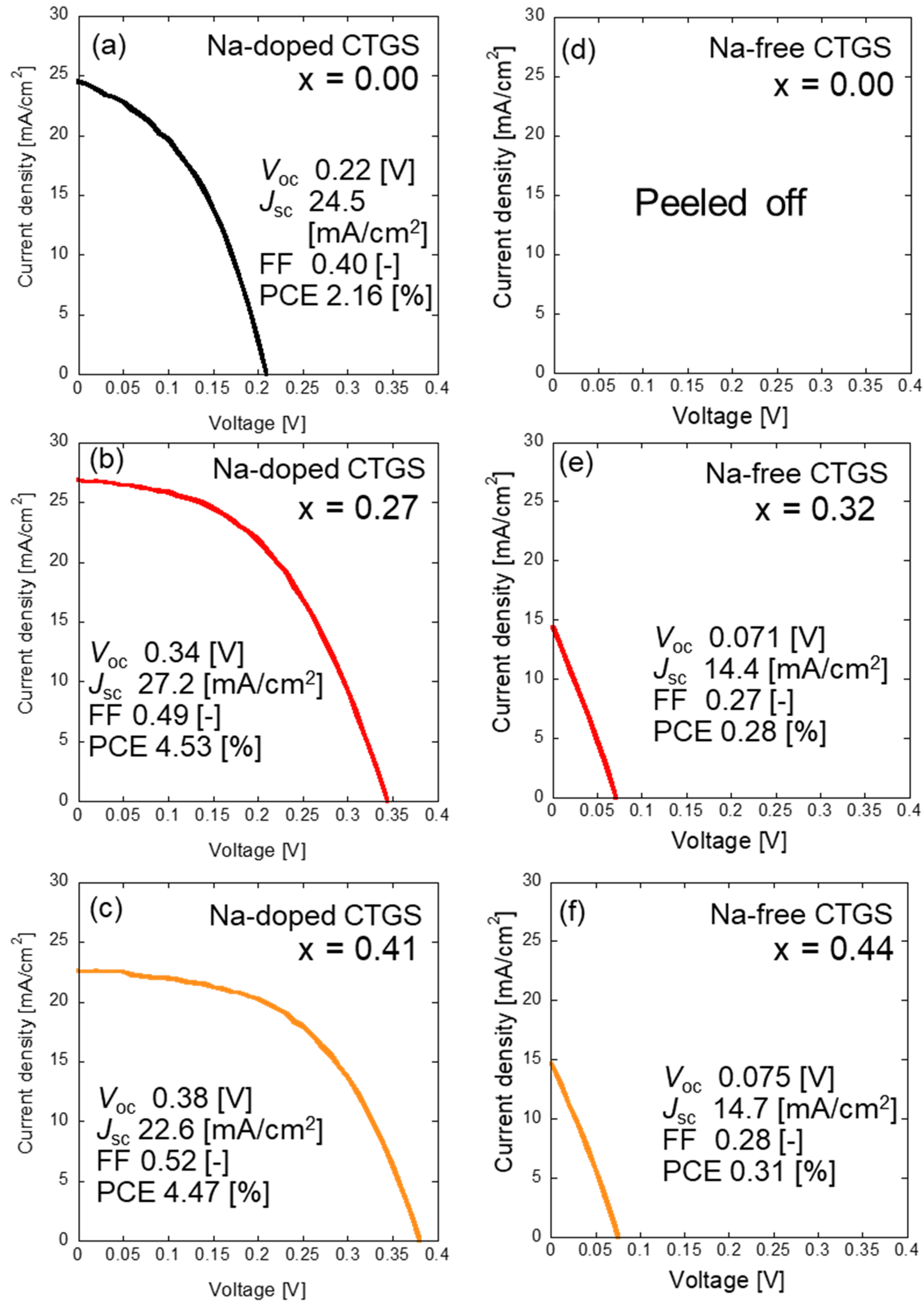
The photovoltaic properties of the solar cells fabricated using these CTGS thin films were studied in detail. Figure 7 shows the measured current density–voltage (J–V) properties of a solar cell based on the fabricated CTGS. The open-circuit voltage (Voc) and short-circuit current density (Jsc) of Na-doped CTGS, shown in Figure 7a–c, are significantly higher than those of Na-free CTGS, shown in Figure 7d–f. This trend is similar to the reported effect of Na doping on CTS solar cells [23]. The poor photovoltaic properties of the Na-free CTGS solar cells could be attributed to the presence of plate-like impurities on the surface (observed in the SEM images), which induce carrier recombination at the p-n interface. Additionally, bulk recombination at the CTGS grain boundaries and/or defects in the CTGS grains possibly contribute to the observed poor performance of the device. In contrast, no impurity is visible on the surface of the Na-doped CTGS thin film. The improved electromotive force characteristics of the device may be attributed to the reduction in photo-excited carrier recombination losses due to the reduction in the grain boundaries during the crystal growth.
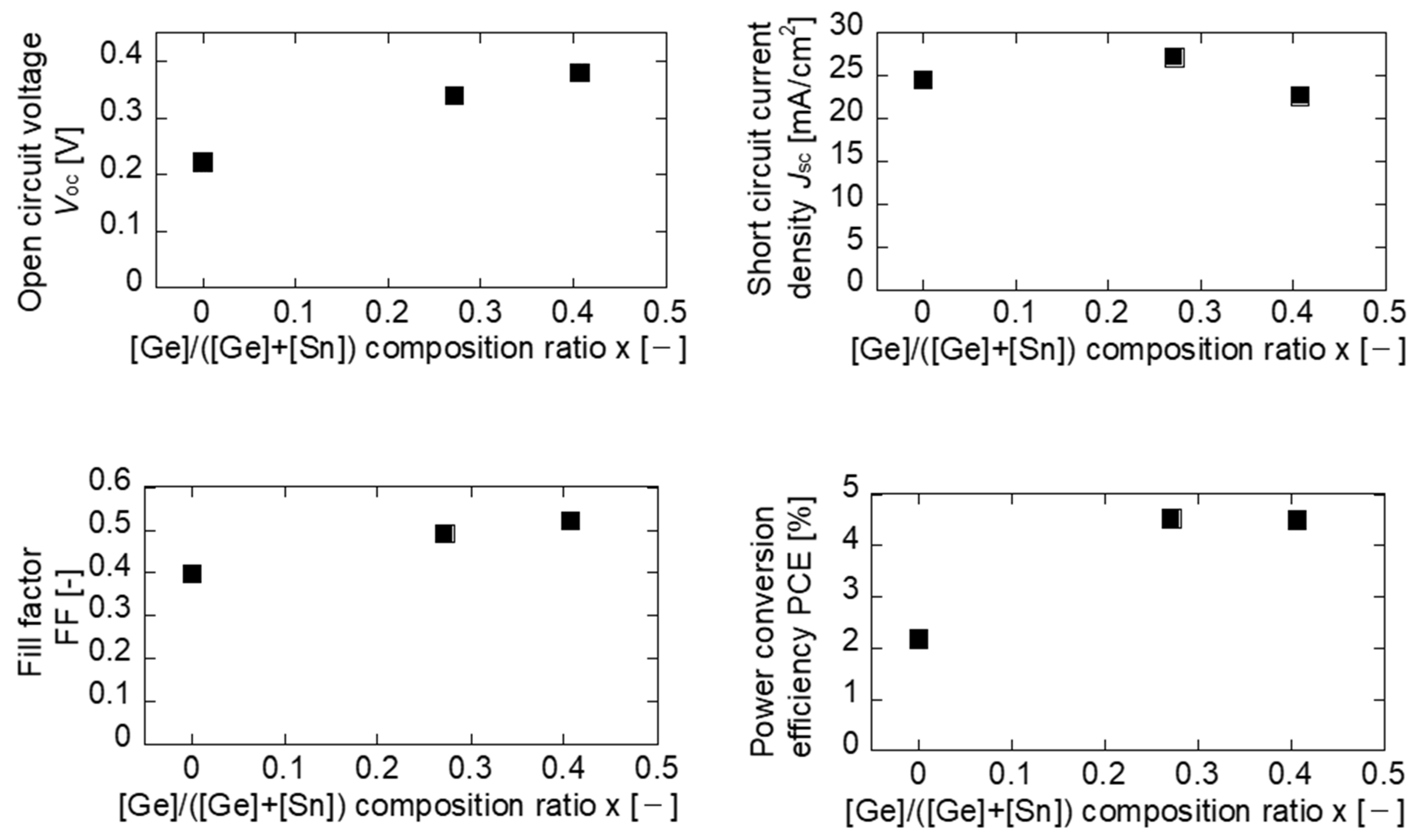
Next, we analyze the dependence of the photovoltaic properties of the fabricated Na-doped CTGS solar cells on x. The x-dependences of Voc, Jsc, fill factor (FF), and PCE of the Na-doped CTGS are shown in Figure 8. The values of Voc at x = 0.27 and 0.41 are higher than that at x = 0.00, and the highest Voc of 0.38 V is obtained at x = 0.41. This increase in Voc is attributed to the widening of the band gap due to Ge alloying. In contrast, Jsc maximizes at x = 0.27 and decreases at x = 0.41. The decrease in Jsc is presumably due to the decrease in the current caused by the increased CTGS band gap. The FF exceeds that at x = 0.00 when both x = 0.27 and 0.41. The PCE of the CTGS solar cells with x = 0.27 and 0.41 is approximately 4.5%, representing a sufficient increase over the efficiency values obtained for the CTS with x = 0.00 by adding Ge and forming a solid solution CTGS.
4. Conclusions
In this study, CTGS thin films were fabricated with a controlled [Ge]/([Ge] + [Sn]) composition ratio x by combining the co-evaporation and sulfurization methods. During the process of fabricating CGS/CTS stacked precursors using the co-evaporation method, the x-value of CTGS was controlled by varying the deposition time of CGS. Furthermore, NaF deposition and sulfurization on the precursor increased the grain size of CTGS, which is similar to previously reported results for CTS. In the solar cell device constructed using the fabricated CTGS thin film, Jsc and Voc improved significantly with Na doping owing to the crystal-growth-promoting effect of Na on CTGS.
Author Contributions
CTGS thin film fabrication, T.T., D.M. and M.T.; Solar cell fabrication of CTS thin film, T.T., D.M. and M.T.; Measurement of CTGS thin films and solar cells, T.T., D.M., M.T. and K.J.; Writing—Original draft preparation, T.T.; Conceptualization, Funding acquisition, Writing—Review and Editing, Supervision, H.A. All authors have read and agreed to the published version of the manuscript.
Funding
This work was partly supported by the Japan Society for the Promotion of Science KAKENHI (grant no. JP19H02663).
Institutional Review Board Statement
Not applicable.
Informed Consent Statement
Not applicable.
Data Availability Statement
Data are contained within the article.
Acknowledgments
The authors gratefully acknowledge Y. Shimamune of the National Institute of Technology, Nagaoka College, for his assistance with the measurements of the J–V characteristics and quantum efficiencies.
Conflicts of Interest
The authors declare no conflicts of interest.
References
- Aihara, N.; Araki, H.; Takeuchi, A.; Jimbo, K.; Katagiri, H. Fabrication of Cu2SnS3 thin films by sulfurization of evaporated Cu-Sn precursors for solar cells. Phys. Status Solidi C 2013, 10, 1086–1092. [Google Scholar] [CrossRef]
- De Chalbaud, L.M.; de Delgado, G.D.; Delgado, J.M. Synthesis and single-crystal structural study of Cu2GeS3. Mater. Res. Bull. 1997, 32, 1371–1376. [Google Scholar] [CrossRef]
- Chen, Q.; Maeda, T.; Wada, T. Optical properties and electronic structures of Cu2SnS3, Cu2GeS3, and their solid solution Cu2(Ge,Sn)S3. Jpn. J. Appl. Phys. 2018, 57, 08RC20. [Google Scholar] [CrossRef]
- Araki, H.; Yamano, M.; Nishida, G.; Takeuchi, A.; Aihara, N.; Tanaka, K. Synthesis and characterization of Cu2Sn1-xGexS3. Phys. Status Solidi C 2017, 10, 1600199. [Google Scholar] [CrossRef]
- Fujita, R.; Saito, N.; Kosugi, K.; Tanaka, K. Preparation of Cu2Sn1-xGexS3 bulk single crystals by chemical vapor transport with iodine. J. Cryst. Growth 2018, 498, 258–262. [Google Scholar] [CrossRef]
- Aihara, N.; Tanaka, K. Photoluminescence characterization of Cu2Sn1-xGexS3 bulk single crystals. AIP Adv. 2018, 8, 095323. [Google Scholar] [CrossRef]
- Peng, X.; Zhang, S.; Xiang, Y. Solvothermal synthesis of Cu2Zn(Sn1-xGex)S4 and Cu2(Sn1-xGex)S3 nanoparticles with tunable band gap energies. J. Alloys Comp. 2015, 640, 75–81. [Google Scholar] [CrossRef]
- Ghorpade, U.V.; Suryawanshi, M.P.; Shin, S.W.; Kim, I.; Ahn, S.K.; Yun, J.H.; Jeong, C.; Kolekar, S.S.; Kim, J.H. Colloidal wurtzite Cu2SnS3 (CTS) nanocrystals and their applications in solar cells. Chem. Mater. 2016, 28, 3308–3317. [Google Scholar] [CrossRef]
- Liu, H.; Xiang, L.; Gao, P.; Wang, D.; Yang, J.; Chen, X.; Li, S.; Shi, Y.; Gao, F.; Zhang, Y. Improvement strategies for stability and efficiency of perovskite solar cells. Nanomaterials 2022, 12, 3295. [Google Scholar] [CrossRef]
- Wang, S.; Li, M.-H.; Jiang, Y.; Hu, J.-S. Instability of solution-processed perovskite films: Origin and mitigation strategies. Mater. Futures 2023, 2, 012102. [Google Scholar] [CrossRef]
- Chantana, J.; Tai, K.; Hayashi, H.; Nishimura, T.; Kawano, Y.; Minemoto, T. Investigation of carrier recombination of Na-doped Cu2SnS3 solar cell for its improved conversion efficiency of 5.1%. Sol. Energy Mater Sol. Cells 2020, 206, 110261. [Google Scholar] [CrossRef]
- Kanai, A.; Sugiyama, M. Na induction effects for J–V properties of Cu2SnS3 (CTS) solar cells and fabrication of a CTS solar cell over-5.2% efficiency. Sol. Energy Mater Sol. Cells 2021, 231, 111315. [Google Scholar] [CrossRef]
- Htay, M.T.; Mandokoro, T.; Seki, H.; Sakaizawa, T.; Momose, N.; Taishi, T.; Hashimoto, Y.; Ito, K. Influence of Ge composition in the Cu2Sn1-xGexS3 thin-film photovoltaic absorber prepared by sulfurization of laminated metallic precursor. Sol. Energy Mater. Sol. Cells 2015, 140, 312–319. [Google Scholar] [CrossRef]
- Hayashi, H.; Chantana, J.; Kawano, Y.; Nishimura, T.; Minemoto, T. Influence of Ge/(Ge+Sn) composition ratio in Cu2Sn1-xGexS3 thin-film solar cells on their physical properties and photovoltaic performances. Sol. Energy Mater Sol. Cells 2020, 208, 110382. [Google Scholar] [CrossRef]
- Umehara, M.; Takeda, Y.; Motohiro, T.; Sakai, T.; Awano, H.; Maekawa, R. Cu2Sn1-xGexS3(x = 0.17) Thin-film solar cells with high conversion efficiency of 6.0%. Appl. Phys. Express 2013, 6, 045501. [Google Scholar] [CrossRef]
- Umehara, M.; Tajima, S.; Aoki, Y.; Takeda, Y.; Motohiro, T. Cu2Sn1−xGexS3 solar cells fabricated with a graded bandgap structure. Appl. Phys. Express 2016, 9, 072301. [Google Scholar] [CrossRef]
- He, M.; Kim, J.; Suryawanshi, M.P.; Lokhande, A.C.; Gang, M.; Ghorpade, U.V.; Lee, D.S.; Kim, J.H. Influence of sulfurization temperature on photovoltaic properties of Ge alloyed Cu2SnS3 (CTGS) thin film solar cells. Sol. Energy Mater. Sol. Cells 2018, 174, 94–101. [Google Scholar] [CrossRef]
- Malaquias, J.C.; Wu, M.; Lin, J.; Robert, E.V.C.; Sniekers, J.; Binnemans, K.; Dale, P.J.; Fransaer, J. Electrodeposition of germanium-containing precursors for Cu2(Sn,Ge)S3 thin film solar cells. Electrochim. Acta 2017, 251, 651–659. [Google Scholar] [CrossRef]
- Araki, H.; Chino, K.; Kimura, K.; Aihara, N.; Jimbo, K.; Katagiri, H. Fabrication of Cu2GeS3-based thin film solar cells by sulfurization of Cu/Ge stacked precursors. Jpn. J. Appl. Phys. 2014, 53, 05FW10. [Google Scholar] [CrossRef]
- Jin, X.; Zhang, L.; Jiang, G.; Liu, W.; Zhu, C. High open-circuit voltage of ternary Cu2GeS3 thin film solar cells from combustion synthesized Cu-Ge alloy. Sol. Energy Mater. Sol. Cells 2017, 160, 319–327. [Google Scholar] [CrossRef]
- Kanai, A.; Araki, H.; Takeuchi, A.; Katagiri, H. Annealing temperature dependence of photovoltaic properties of solar cells containing Cu2SnS3 thin films produced by co-evaporation. Phys. Status Solidi B 2015, 252, 1239–1243. [Google Scholar] [CrossRef]
- Kanai, A.; Toyonaga, K.; Chino, K.; Katagiri, H.; Hideaki, A. Fabrication of Cu2SnS3 thin-film solar cells with power conversion efficiency of over 4%. Jpn. J. Appl. Phys. 2015, 54, 08KC06. [Google Scholar] [CrossRef]
- Sasagawa, S.; Nishida, G.; Takeuchi, A.; Katagiri, H.; Hideaki, A. Effect of sodium addition on Cu2SnS3 thin-film solar cells fabricated on alkali-free glass substrates. Jpn. J. Appl. Phys. 2018, 57, 08RC11. [Google Scholar] [CrossRef]
- Sasagawa, S.; Yago, A.; Kanai, A.; Araki, H. Cu2(Sn1-xGex)S3 solar cells prepared via co-evaporation and annealing in germanium sulfide and sulfur vapor. Phys. Status Solidi C 2017, 14, 1600193. [Google Scholar] [CrossRef]
- Kanai, A.; Araki, H.; Ohashi, R.; Sugiyama, M. Sulfurization of Cu2(Sn,Ge)S3 thin films deposited by co-evaporation. Jpn. J. Appl. Phys. 2020, 59, SCCD01. [Google Scholar] [CrossRef]
- Green, M.A.; Dunlop, E.D.; Yoshita, M.; Kopidakis, N.; Bothe, K.; Siefer, G.; Hao, X. Solar cell efficiency tables (Version 63). Prog. Photovolt. 2024, 32, 3–13. [Google Scholar] [CrossRef]
- Scarpulla, M.A.; McCandless, B.; Phillips, A.B.; Yan, Y.; Heben, M.J.; Wolden, C.; Xiong, G.; Metzger, W.K.; Mao, D.; Krasikov, D.; et al. CdTe-based thin film photovoltaics: Recent advances, current challenges and future prospects. Sol. Energy Mater. Sol. Cells 2023, 255, 112289. [Google Scholar] [CrossRef]
- Huang, C.-H.; Chuang, W.-J.; Lin, C.-P.; Jan, Y.-L.; Shih, Y.-C. Deposition technologies of high-efficiency CIGS solar cells: Development of two-step and co-evaporation processes. Crystals 2018, 8, 296. [Google Scholar] [CrossRef]
- Hamamura, K.; Chantana, J.; Suzuki, K.; Minemoto, T. Influence of Cu/(Ge + Sn) composition ratio on photovoltaic performances of Cu2Sn1-xGexS3 solar cell. Sol. Energy 2017, 149, 341–346. [Google Scholar] [CrossRef]
- Nikolaev, R.E.; Vasilyeva, I.G. A new way of phase identification, of AgGaGeS4∙nGeS2 crystals. J. Solid State Chem. 2013, 203, 340. [Google Scholar] [CrossRef]
- Piacente, V.; Foglia, S.; Scardala, P. Sublimation study of the tin sulphides SnS2, Sn2S3 and SnS. J. Alloys Comp. 1991, 177, 17–30. [Google Scholar] [CrossRef]
- Ye, Q.; Xu, D.; Cai, B.; Lu, J.; Yi, H.; Ma, C.; Zheng, Z.; Yao, J.; Ouyang, G.; Yang, G. High-performance hierarchical O-SnS/I-ZnIn2S4 photodetectors by leveraging the synergy of optical regulation and band tailoring. Mater. Horiz. 2022, 9, 2364–2375. [Google Scholar] [CrossRef] [PubMed]
- Pyeon, J.J.; Baek, I.-H.; Song, Y.G.; Kim, G.S.; Cho, A.-J.; Lee, G.-Y.; Han, J.H.; Chung, T.-M.; Hwang, C.S.; Kang, C.-Y.; et al. Highly sensitive flexible NO2 sensor composed of vertically aligned 2D SnS2 operating at room temperature. J. Mater. Chem. C 2020, 8, 11874–11881. [Google Scholar] [CrossRef]
- Suzuki, K.; Chantana, J.; Minemoto, T. Na role during sulfurization of NaF/Cu/SnS2 stacked precursor for formation of Cu2SnS3 thin film as absorber of solar cell. Appl. Surf. Sci. 2017, 414, 140–146. [Google Scholar] [CrossRef]
Figure 1.
Schematic of the CTGS-based solar cell fabrication process.

Figure 2.
Relationship between x before and after sulfurization of obtained thin films. The horizontal axis represents x before sulfurization, and the vertical axis represents x after sulfurization. The dotted line represents the case in which no difference in composition exists between before and after.
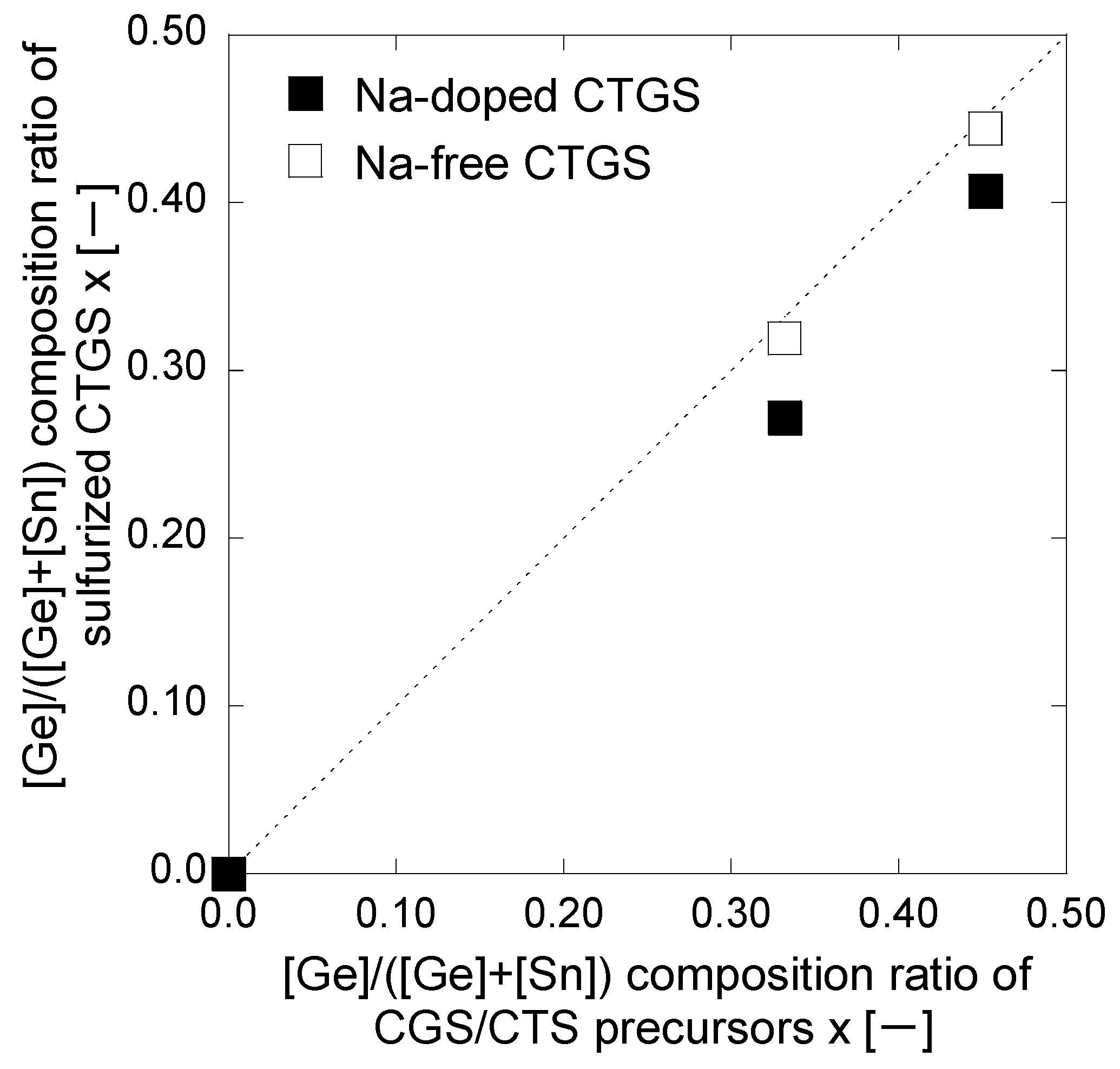
Figure 3.
(a) XRD spectra for Na-doped CTGS samples with varying values of x. (b) XRD spectra for Na non-doped CTGS with varying x.
Figure 3.
(a) XRD spectra for Na-doped CTGS samples with varying values of x. (b) XRD spectra for Na non-doped CTGS with varying x.

Figure 4.
(a) Magnified XRD spectra near the (200) plane of monoclinic-CTS and monoclinic-CGS in Na-doped CTGS and (b) magnified XRD spectra of Na-free CTGS. Arrows indicate the position of the maximum peak intensity of the diffraction peaks corresponding to the (200) plane in CTS and CTGS.
Figure 4.
(a) Magnified XRD spectra near the (200) plane of monoclinic-CTS and monoclinic-CGS in Na-doped CTGS and (b) magnified XRD spectra of Na-free CTGS. Arrows indicate the position of the maximum peak intensity of the diffraction peaks corresponding to the (200) plane in CTS and CTGS.
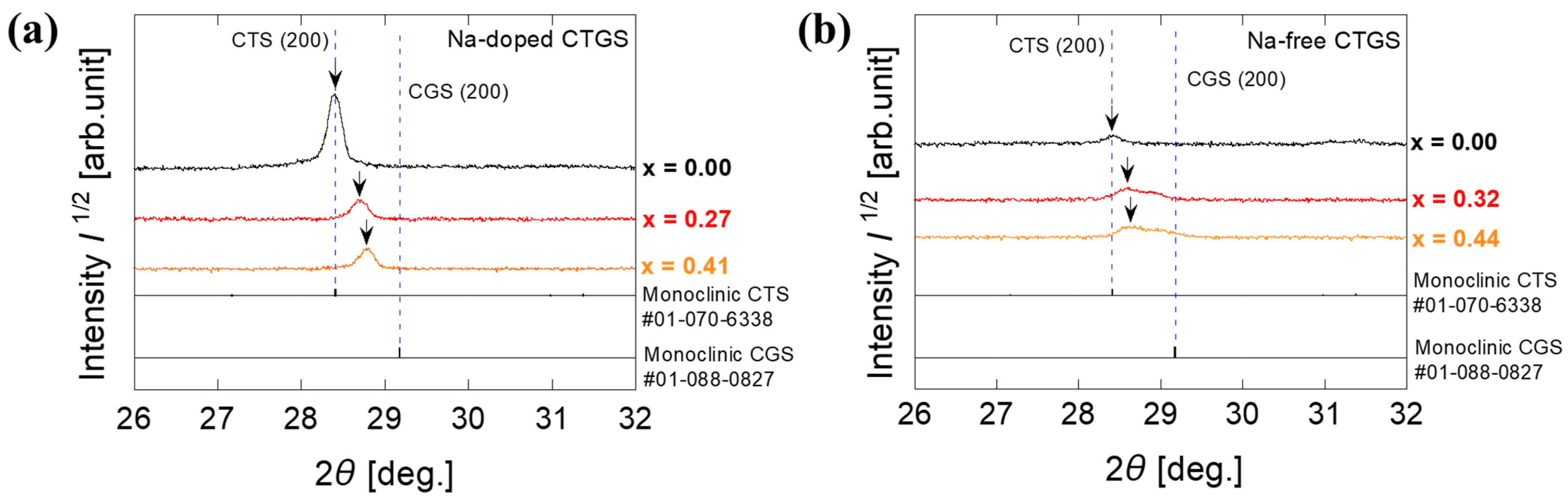
Figure 5.
Open and closed circles represent the angles of the peaks corresponding to the (200) plane of the CTS (PDF #01-070-6338) at x = 0 and the CGS (PDF #01-088-0827) at x = 1, respectively. The dotted line connecting them represents the expected diffraction angle of the (200) plane relative to the Ge composition x-value based on Vegard’s law. The open and closed squares represent the diffraction angles of the peak corresponding to the (200) plane of Na-free CTGS and Na-doped CTGS relative to the Ge composition x-value, respectively.
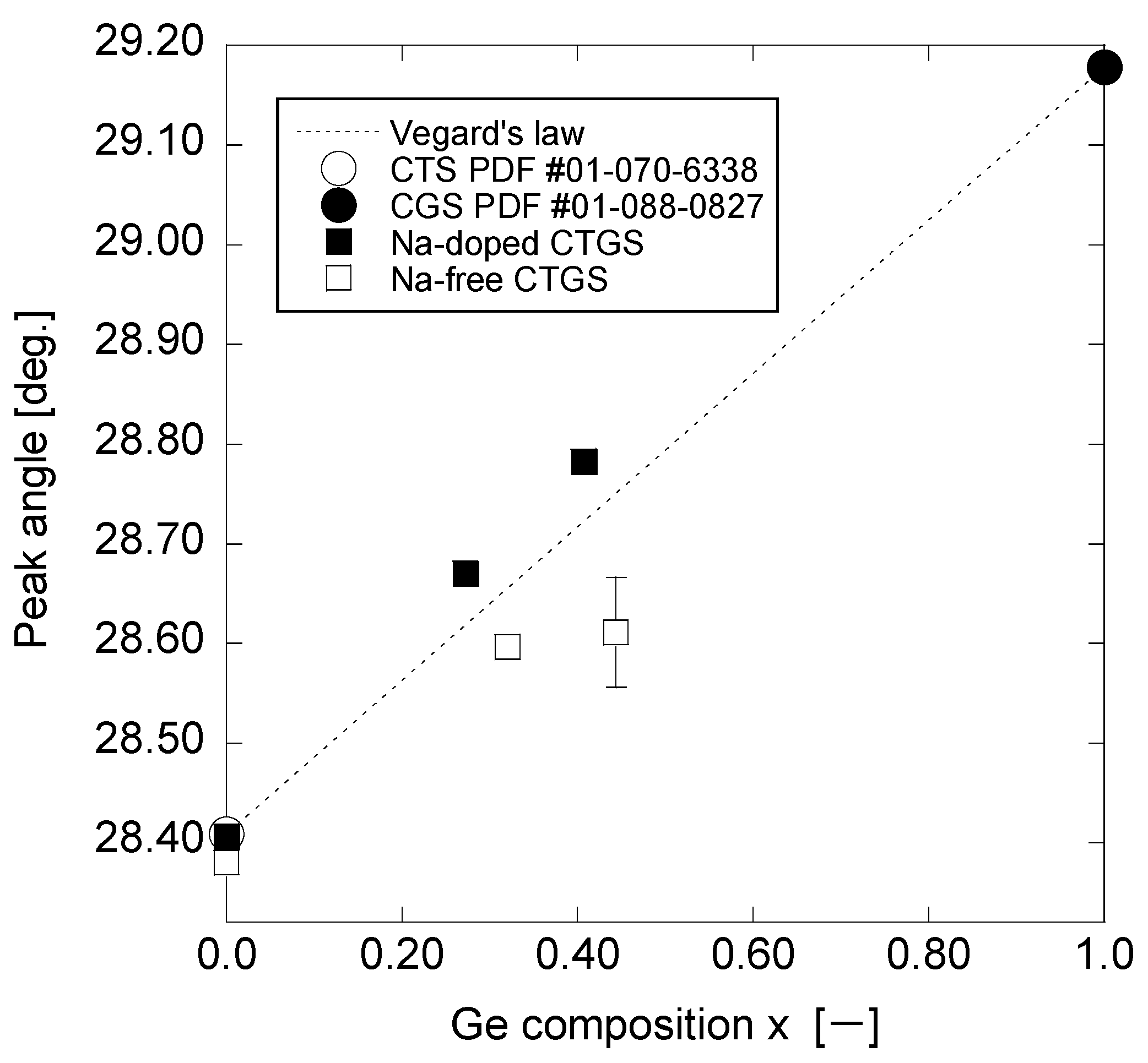
Figure 6.
Surface and cross-sectional SEM images of Na-doped and Na-free CTGS.

Figure 7.
J–V curves of the cells showing the best photovoltaic characteristics among the CTGS solar cells fabricated for each condition. Photovoltaic properties of (a–c) Na-doped CTGS solar cells and (d–f) Na-free CTGS solar cells.
Figure 7.
J–V curves of the cells showing the best photovoltaic characteristics among the CTGS solar cells fabricated for each condition. Photovoltaic properties of (a–c) Na-doped CTGS solar cells and (d–f) Na-free CTGS solar cells.

Figure 8.
The x-dependence of photovoltaic properties in Na-doped CTGS solar cells.

Table 1.
Reported fabrication methods of CTS, CGS, and CTGS thin-film solar cells; range of [Ge]/([Ge] + [Sn]) composition ratios; and PCEs.
Table 1.
Reported fabrication methods of CTS, CGS, and CTGS thin-film solar cells; range of [Ge]/([Ge] + [Sn]) composition ratios; and PCEs.
| Precursor | Method | [Ge]/([Ge] + [Sn]) | PCE [%] | Ref. |
|---|---|---|---|---|
| Soda lime glass (SLG)/Mo/Cu-SnS2/NaF | Sputtering and annealing with S and SnS | 0 | 5.1 | [11] |
| SLG/Mo/Cu/SnS2/NaF | Sputtering and annealing with S | 0 | 5.2 | [12] |
| SLG/Mo/Ge, Sn, and Cu laminated layers | Sputtering and annealing with S in a closed tube | 0–1.0 | ~2 | [13] |
| SLG/Mo/Ge/Cu–SnS2 | Sputtering and annealing with S and SnS2 | 0–0.58 | 5.6 | [14] |
| SLG/Mo/Cu–Sn | Co-sputtering and annealing with S and GeS2 | 0, 0.17 | 6.0 | [15] |
| SLG/Mo/Cu–Sn | Co-sputtering and annealing with S and GeS2 | Graded band gap structure | 6.7 | [16] |
| SLG/Mo/Sn/Ge/Cu | Sputtering and annealing with S | 0.061–0.110 | 2.14 | [17] |
| SLG/Mo/Cu(Sn,Ge) | Electrodeposition and annealing with S and GeS | 0.83 | 0.7 | [18] |
| SLG/Mo/Cu/Ge | Evaporation and annealing with S | 1.0 | 1.70 | [19] |
| SLG/Mo/Cu–Ge | Annealing of Cu-Ge alloy prepared by combustion method with S | 1.0 | 2.67 | [20] |
Table 2.
Composition ratios (x) of CGS/CTS stacked precursor and sulfurized CTGS measured using XRF. Sulfurized CTGS was designated as Na-doped CTGS and Na-free CTGS, respectively, depending on the presence or absence of NaF during sulfurization.
Table 2.
Composition ratios (x) of CGS/CTS stacked precursor and sulfurized CTGS measured using XRF. Sulfurized CTGS was designated as Na-doped CTGS and Na-free CTGS, respectively, depending on the presence or absence of NaF during sulfurization.
| tCGS [h] | [Cu]/([Ge] + [Sn]) | [Ge]/([Ge] + [Sn]) x | [S]/([Cu] + [Ge] + [Sn]) | |
|---|---|---|---|---|
| CGS/CTS precursor | 0.0 | 1.58 | 0.00 | 1.07 |
| 1.0 | 1.67 | 0.33 | 1.00 | |
| 1.5 | 1.68 | 0.45 | 0.98 | |
| Na-doped CTGS | 0.0 | 1.60 | 0.00 | 1.15 |
| 1.0 | 1.91 | 0.27 | 1.26 | |
| 1.5 | 1.94 | 0.41 | 1.16 | |
| Na-free CTGS | 0.0 | Peeled off | Peeled off | Peeled off |
| 1.0 | 1.80 | 0.32 | 1.07 | |
| 1.5 | 1.81 | 0.44 | 1.07 |
Disclaimer/Publisher’s Note: The statements, opinions and data contained in all publications are solely those of the individual author(s) and contributor(s) and not of MDPI and/or the editor(s). MDPI and/or the editor(s) disclaim responsibility for any injury to people or property resulting from any ideas, methods, instructions or products referred to in the content. |
© 2024 by the authors. Licensee MDPI, Basel, Switzerland. This article is an open access article distributed under the terms and conditions of the Creative Commons Attribution (CC BY) license (https://creativecommons.org/licenses/by/4.0/).
Share and Cite
MDPI and ACS Style
Tasaki, T.; Jimbo, K.; Motai, D.; Takahashi, M.; Araki, H. Fabrication of Cu2Sn1-xGexS3 Thin-Film Solar Cells via Sulfurization of Cu2GeS3/Cu2SnS3 Stacked Precursors. Materials 2024, 17, 1886. https://doi.org/10.3390/ma17081886
AMA Style
Tasaki T, Jimbo K, Motai D, Takahashi M, Araki H. Fabrication of Cu2Sn1-xGexS3 Thin-Film Solar Cells via Sulfurization of Cu2GeS3/Cu2SnS3 Stacked Precursors. Materials. 2024; 17(8):1886. https://doi.org/10.3390/ma17081886
Chicago/Turabian StyleTasaki, Takeshi, Kazuo Jimbo, Daiki Motai, Masaya Takahashi, and Hideaki Araki. 2024. "Fabrication of Cu2Sn1-xGexS3 Thin-Film Solar Cells via Sulfurization of Cu2GeS3/Cu2SnS3 Stacked Precursors" Materials 17, no. 8: 1886. https://doi.org/10.3390/ma17081886
Note that from the first issue of 2016, this journal uses article numbers instead of page numbers. See further details here.