3. Results and Discussion
Theoretical modeling is essential prior to any experimental investigation, in order to fully understand the various physical phenomena at play and optimize structure parameters. The theoretical modeling, presented herein, considers the case of an extremely thin (5 nm) FSP layer coated on a ZnO thin film grown on a sapphire substrate. The Source-Terms method is applied in order to model the emission of the FSP layer and ZnO thin film [
18,
32]. The applied model was shown to present good agreement with experimental results [
33].
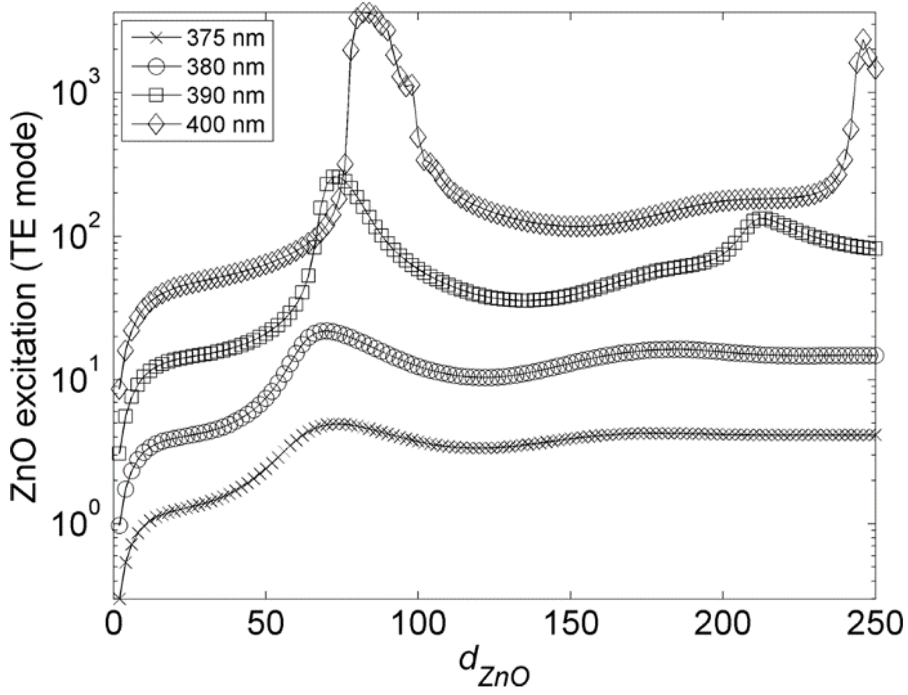
Figure 3 presents the evolution of the ZnO excitation of the FSP layer (
i.e., the intensity of the ZnO emission inside the FSP layer) as a function of the ZnO film thickness (
dZnO). The graphs presented in
Figure 3 are normalized to
dZnO = 0 and shifted by half an order of magnitude in the
y-axis. Since ZnO emission is preferably TE-polarized [
33,
34], only the TE mode was considered in the calculations. Calculations were carried out at the wavelengths of 375 nm (×), 380 nm (○), 390 nm (□), and 400 nm (◊), in order to account for the spectral redshift which occurs in ZnO emission when it passes from a spontaneous emission regime (at 375 nm) to a stimulated emission regime (
cf. Section 2.3).
Figure 3.
Evolution of the ZnO excitation as a function of the ZnO layer thickness (
dZnO) and emission wavelength. Graphs are shifted by half an order of magnitude and normalized to
dZnO = 0. Reprinted with permission from [
18]. Copyright 2010 AIP Publishing LLC.
Figure 3.
Evolution of the ZnO excitation as a function of the ZnO layer thickness (
dZnO) and emission wavelength. Graphs are shifted by half an order of magnitude and normalized to
dZnO = 0. Reprinted with permission from [
18]. Copyright 2010 AIP Publishing LLC.
Figure 3 reveals that a ZnO excitation optimum exists for each of the considered wavelengths. Optimum ZnO excitation occurs for thicknesses of
dZnO = λ
ZnO/2
nZnO, where λ
ZnO and
nZnO are respectively the emission wavelength and refractive index of the ZnO thin film. At these thicknesses, the ZnO thin film is a single-mode waveguiding slab.
Figure 3 shows that the gradual redshift of the ZnO emission from 375 nm to 400 nm results in a drastic increase in the ZnO excitation. This is due to the emphasis of the guided mode [
18], as the extinction coefficient (κ) is reduced from 0.311 at 375 nm to 0.004 at 400 nm [
30].
Figure 3 shows that guided ZnO emission has more important impact on the FSP layer excitation compared to the outwards-emitted ZnO emission. ZnO guided emission provides the most efficient way to excite the FSP layer, as it allows for the FSP layer to be repeatedly excited via the tail of the evanescent wave.
In order to experimentally validate the G-WET, extremely thin (10 nm) FSP (
cf. Section 2.2) layers were spincoated on a quartz substrate (sample denoted S0) and a 170 nm thick ZnO thin film grown on sapphire (sample denoted S1) [
19]. The samples were excited using a pulsed nitrogen laser (λ = 337.1 nm, 4 ns pulse duration) operating at a repetition rate of 10 Hz. Polymer fluorescence was collected using an objective lens with a 0.13 numerical aperture focused onto a large core (400 µm diameter) optical fiber connected to a 50 cm focal length spectrometer equipped with a CCD Peltier-cooled camera. Neutral density filters were used in order to control the pumping intensity.
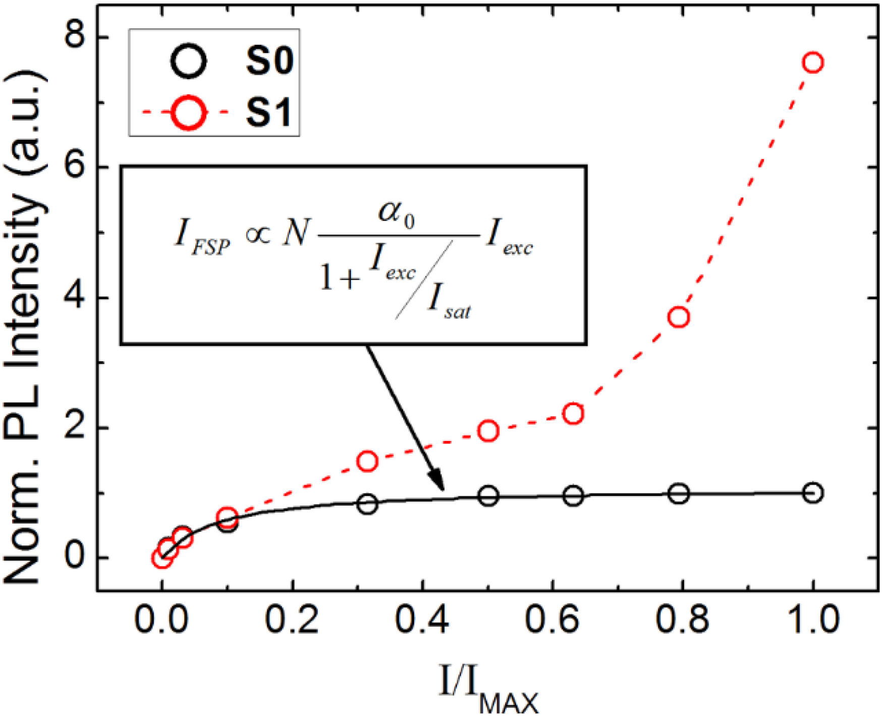
Figure 4 presents the evolution of the FSP peak intensity (λ = 468 nm) for S0 and S1 samples as a function of the normalized pumping intensity (
I/
IMAX). Peak intensities are normalized to the maximum peak intensity presented by S0 (
i.e., at
I/
IMAX = 1).
Figure 4 shows that the FSP layer coated on quartz (
i.e., S0) saturates in the fluorescence peak intensity (black circles) at high pumping intensities according to the formula in insert. The fluorescence saturation of S0 is attributed to the absorption saturation of the FSP layer lying under direct laser excitation [
19].
Figure 4.
Comparison between the photoluminescence of the fluorescent polymer film coated on quartz, S0 sample (black circles) and on the ZnO layer, S1 sample (green circles) as a function of the normalized pumping intensity (
I/
IMAX). The plotted PL intensity values are taken at λ ~ 468 nm and normalized by the maximum PL intensity recorded for the S0 sample. Reprinted with permission from [
19]. Copyright 2014 American Chemical Society.
On the other hand,
Figure 4 reveals that the FSP layer coated on ZnO (
i.e., S1) exhibits a superlinear (2.5 power) increase in fluorescence peak intensity (red circles) at high pumping intensities, eventually reaching an 8-fold enhancement compared to S0. Experimental investigations [
19] show that the superlinear dependence of the FSP fluorescence is tightly linked to stimulated ZnO plasma emission (
i.e.,
N-line), proving the occurrence of a radiative energy transfer from the ZnO thin film towards the FSP layer.
The fluorescence enhancement, in the case of S1, is attributed to an efficient excitation of the polymer layer lying outside of the area defined by the laser spot via the waveguided ZnO stimulated emission (
i.e., a “geometrical” effect). The geometrical effect is confirmed by photoluminescence (PL) measurements shown in
Figure 5.
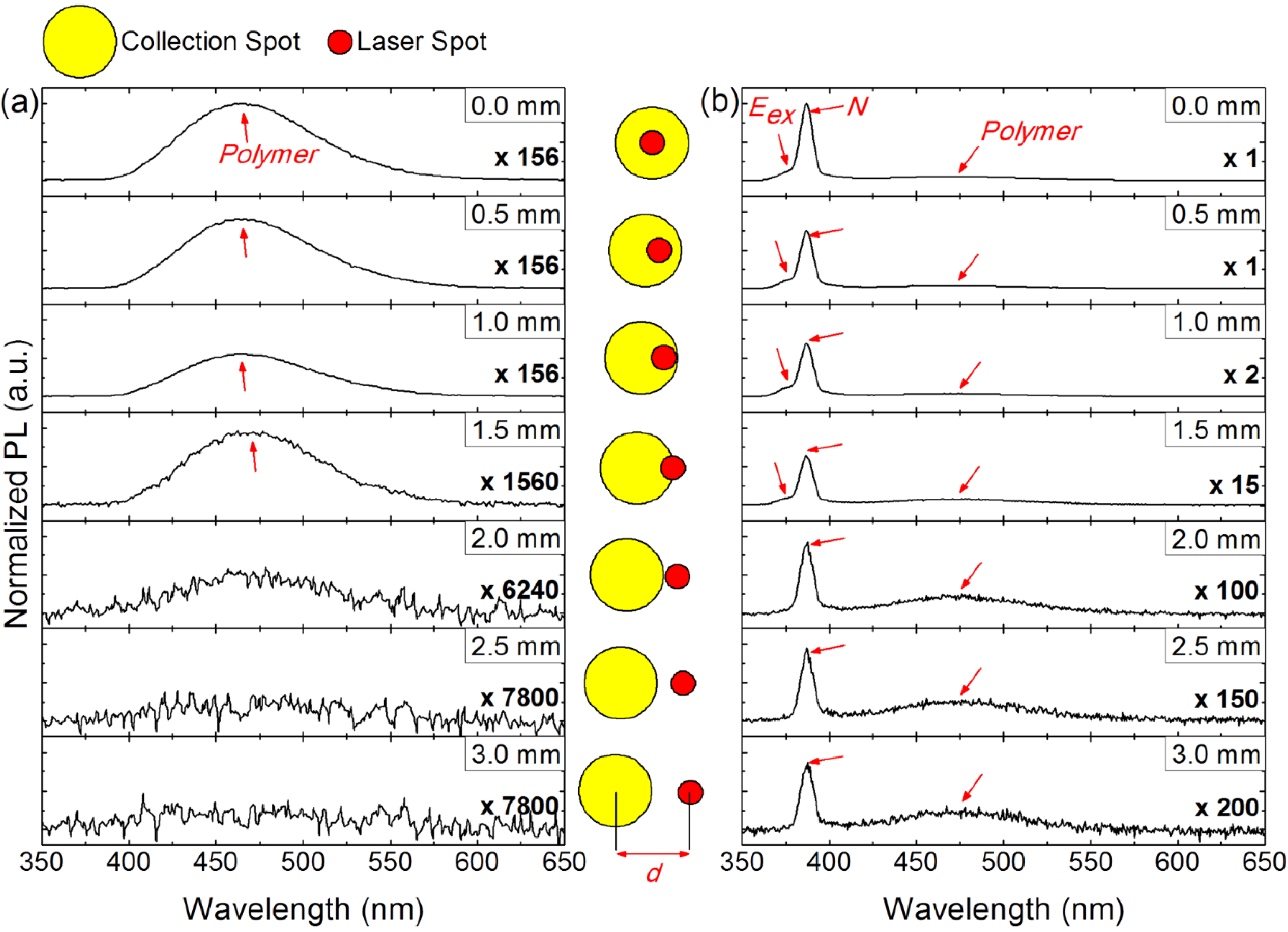
Figure 5.
Evolution of the photoluminescence (PL) spectra for the polymer fluorescent film coated on quartz, S0 sample (
a) and on the ZnO layer, S1 sample (
b) as a function of the distance (
d) separating the center laser spot and the axis of the collection objective. The PL spectra are all plotted on the same
y-axis scale and normalized by the PL intensity recorded at the maximum emission wavelength of the
N-line for
d = 0 mm. The inset between the two figures presents a sketch of the evolution of d. Reprinted with permission from [
19]. Copyright 2014 American Chemical Society.
Figure 5 shows the evolution of the PL spectra collected on S0 (a) and S1 (b) as the misalignment (
d) between the collection axis and the laser spot is gradually increased. The value of
d is indicated in the legend of each graph and is illustrated in the inset of
Figure 5. The PL setup, considered here, has a collection spot area diameter of 3 mm and a laser spot diameter of 1mm. At
d = 2 mm, the collection spot is thus externally tangent to the laser spot, as illustrated in
Figure 5.
Figure 5a shows that, in the case of S0, the fluorescent polymer area is solely defined by the laser spot. In fact, the polymer fluorescence spectrum, as shown in
Figure 5a, totally vanishes for
d ≥ 2 mm. For S0, the polymer layer is uniquely excited by the laser beam. On the other hand,
Figure 5b clearly shows that, in the case of S1, the fluorescent polymer area is strictly larger than that of the laser spot. For S1, the polymer fluorescence spectrum, as shown in
Figure 5b, is still collected for
d ≥ 2 mm. The polymer fluorescence, in the case of S1, results of two fluorescing areas. A smaller area, defined by the laser spot (depicted by the dark green star in
Figure 1b), that is mainly excited by the laser beam; and a larger area, defined outside of the laser spot (depicted by the light green in
Figure 1b), that is mainly excited by the waveguided ZnO stimulated plasma
N-line emission at 386 nm. This is evidenced by the
N-line peak collected at
d ≥ 2 mm. Meanwhile, the spectral filtering (
i.e., attenuation) for
d ≥ 2 mm of the ZnO spontaneous emission at 375 nm, denoted by
Eex, evidences on the waveguided nature of the
N-line (the extinction coefficient κ of ZnO is decreased from 0.311 at 375 nm to 0.056 at 386 nm).
The experimental investigation reveal almost one order of magnitude fluorescence enhancement by spincoating the FSP on a ZnO thin film. Furthermore, the experimental investigation proves the important role of waveguided ZnO emission in having an efficient fluorescence excitation of extremely thin FSP layers. The experimental results are in good agreement with the previously discussed theoretical results which also revealed the importance of waveguided ZnO emission. However, the theoretical modeling predicted a 30-fold enhancement of the polymer fluorescence. The prediction is overestimated mainly due to the fact that the theoretical modeling did not account for the real values of the polymer and ZnO quantum yield.
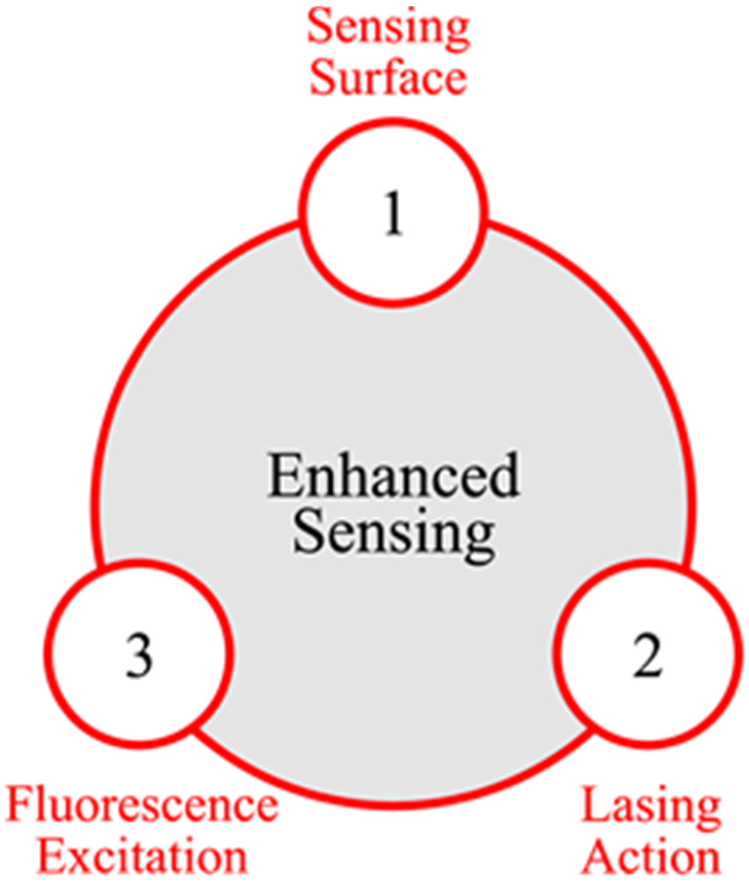
As previously mentioned, nanostructured materials present many interesting properties which can be extremely beneficial for sensing applications. In the following, we present a preliminary theoretical study on the enlarged sensing surface and photonic band-gap of ZnO nanostructures. The theoretical study, presented henceforth, considers the case of hexagonally distributed ZnO nanorods and perforated ZnO thin films. Hexagonal distribution is chosen as it presents the most compact packing arrangement and therefore the most interesting geometric and photonic properties.
Nanostructured materials can exhibit extremely high specific surfaces which can help increase polymer sensitivity by enlarging the polymer sensing surface and enhancing fluorescence signal without diminishing their response time and quenching efficiency [
16]. We define the gain in sensing surface (
RG) as the ratio between the surface area of a FSP layer coated on a nanostructured support and that of a FSP layer coated on a smooth plan. Considering a homogeneous FSP coating over the whole coated area,
RG, of any given geometry, can be determined through simple geometrical calculations.
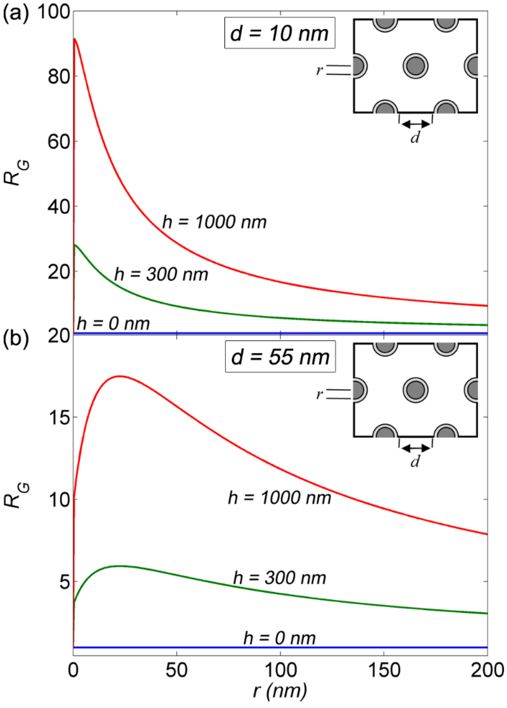
Figure 6 represents the evolution of
RG for a hexagonal array of nanorods as a function of the rods radius (
r) for various rod heights (
h = 0 nm, 300 nm, and 1000 nm) and for two fixed values of the air gap (
d = 10 nm (a) and 55 nm (b)) separating two adjacent polymer coated nanorods (see
Figure 6 inset). For the figure insets hereafter grey is for ZnO and white is for air. The calculated values of
RG are obtained for a fixed polymer thickness of 5 nm. As shown in
Figure 6a,b, for
h = 0 or
r = 0 (
i.e., no nanorods), the surface presents no gain and, as expected,
RG has a value of 1. However, for any given value of
h and
r differing from 0,
RG presents a value higher than 1. In other words, any array of nanorods, no matter the structure parameters, will exhibit an enlarged sensing surface compared to a smooth plane. In general,
Figure 6 shows that the enlarged sensing surface (
i.e.,
RG) is more important for a higher (
i.e., increasing
h) and denser (
i.e., decreasing
d) stacking of nanorods. For
h > 0,
RG exhibits an optimum value. As seen in
Figure 6a,b, the optimum value of
RG shifts towards higher values of
r as
d increases. For the considered structure parameters, the highest calculated value for
RG reaches a value of ~90 (almost two order of magnitude) and is obtained for
r ≈ 0.4 nm,
d = 10 nm and
h = 1000 nm. For
d = 10 nm (
Figure 6a), the optimum value of
RG exists at the smallest value of
r ≠ 0, which results in a very abrupt change from
RG = 1 at
r = 0 to
RG ≈ 90 at
r ≈ 0.4. Nonetheless, nanorods of such high aspect ratio (
r ≈ 0.4 nm and
h = 1000 nm) are experimentally hard to realize. More reasonable structure parameters, such as
r = 50 nm,
d = 55 nm and
h = 1000 nm, reduces the surface gain to an order of a 15-fold (one order of magnitude). Nonetheless, this remains an important enhancement factor. It is essential to stress that a facile technique for the growth of urchin-like ZnO nanostructures was recently reported by our team [
35]. The grown urchin-like structures exhibited a high aspect ratio with ZnO nanorods of a diameter of around 15 nm and a length of 500 nm. With such dimensions, the urchin-like nanostructures should result in a gain in sensing surface of more than two-orders of magnitude as compared to a flat surface. Moreover, the urchin-like nanostructures exhibited a high internal quantum efficiency of 23% at room temperature. The luminescence properties of urchin-like nanostructures are thus also potentially interesting for achieving an efficient G-WET.
Figure 6.
Evolution of the surface gain (RG) for hexagonally ordered ZnO nanorods as a function of the radius (r) and for various nanorod height (h). (a) presents the case of d = 10 nm and (b) presents the case of d = 55 nm.
Figure 6.
Evolution of the surface gain (RG) for hexagonally ordered ZnO nanorods as a function of the radius (r) and for various nanorod height (h). (a) presents the case of d = 10 nm and (b) presents the case of d = 55 nm.
In analogy to
Figure 6,
Figure 7 represents the evolution of
RG for a hexagonal array of nanoholes, perforated in a ZnO thin film, as a function of the nanoholes radius
r for various values of film thicknesses (
h = 0 nm, 300 nm, and 1000 nm) and for two fixed values of the air gap (
d = 10 (a) and 55 nm (b)) separating two adjacent polymer coated nanoholes (see
Figure 7 inset). The polymer thickness is again fixed to 5 nm. The calculated values of
RG for the nanoholes, shown in
Figure 7, exhibit a similar behavior to the calculated values of
RG for the nanorods, shown in
Figure 6. As seen in
Figure 7, gains in sensing surface are expected independently of structures parameters (
i.e.,
RG is bigger than 1 for any value of
r and
h differing from 0). Moreover, the enlarged sensing surface (
i.e.,
RG) is more important for a deeper (
i.e., increasing
h) and denser (
i.e., decreasing
d) stacking of nanoholes. However, perforated thin films, in general, present smaller values of
RG compared to nanorods. The highest
RG calculated for perforated thin films reaches a value of ~45 for
r ≈ 15 nm,
d = 10 nm and
h = 1000 nm. However, arrays of nanoholes with such dimensions are hard to perforate, especially in ZnO thin films. Moreover, nanoholes with such radius (
r ≈ 15) are hard to homogeneously coat with a polymer, due to the limited polymer penetration inside the holes (surface wetting problem). Again, more feasible nanoholes [
20] lead to a 15-fold enhancement (one order of magnitude) in the sensing surface.
Figure 7.
Evolution of the surface gain (RG) for hexagonally ordered nanoholes as a function of the radius (r) and for various nanorod heights (h). (a) presents the case of d = 10 nm and (b) presents the case of d = 55 nm.
Figure 7.
Evolution of the surface gain (RG) for hexagonally ordered nanoholes as a function of the radius (r) and for various nanorod heights (h). (a) presents the case of d = 10 nm and (b) presents the case of d = 55 nm.
As previously mentioned, optical gain is an essential feature of the G-WET concept. It is clear that higher optical gains and reduced lasing thresholds are desirable for more efficient energy transfers. ZnO micro- and nanostructures can be thus important for such purposes. We recently showed [
21] that ZnO microdisks exhibited a reduced lasing threshold compared to the initial lasing threshold measured for the ZnO thin film before microstructuring. The reduced lasing threshold was attributed to the optical feedback occurring inside the microstructures. Such structures are extremely interesting as they are easy to realize, especially at a large scale, and they should allow for an efficient G-WET process at low pumping intensities. On the other hand, templated growth offers an easy and cheap alternative for the realization of nanostructures. Recent advances on assisted sphere self-assembly in our team allow for the realization of hexagonally ordered ZnO nanostructures on a large scale [
36]. Such large scale and cheap ZnO nanostructuring is interesting for many functional applications including sensors.
Hexagonal arrays of ZnO nanostructures are photonic crystals (PhCs) and thus present interesting photonic properties. Recent studies have shown that the photonic band-gap (PBG) plays a crucial role in reducing the lasing threshold in ZnO PhCs [
20]. Therefore, it is essential to determine the structure parameters that are required to obtain the desired PBG. For this purpose, plane wave expansion (PWE) calculations [
37,
38] were carried out using a photonics design automation software ‘RSoft’. PWE method offers a fast and accurate technique to determine the photonic band diagram, and therefore the PBG, of PhCs. Before proceeding, it is essential to note that, hereafter, transverse magnetic (TM) polarization is defined as the electric field being parallel to the rods/holes; while transverse electric (TE) polarization is define as the electric field running around the rods/holes.
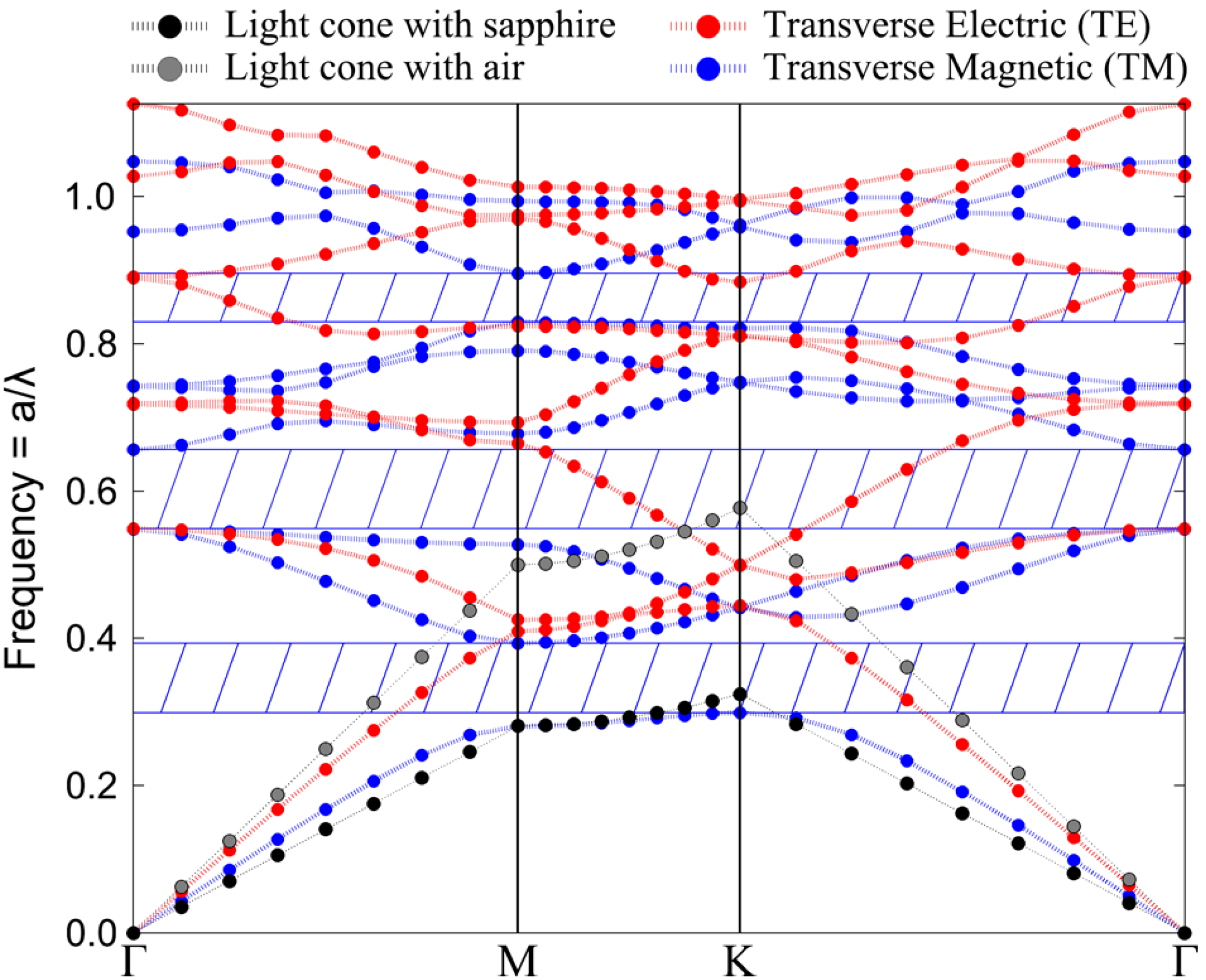
Figure 8 shows the photonics band diagram obtained at λ = 375 nm for a hexagonal distribution of ZnO nanorods having radius on period ratio (
r/
a) of 0.3. The
x-axis represents the wave-vector
k (
kx,
ky), where Γ (0,0), M (π/
a,
), and K (4π/3
a, 0) are the symmetry points of the hexagonal lattice in reciprocal space.
Figure 8 shows that the considered ZnO nanorods structure parameters exhibit 3 TM-polarized PBGs. It is important to note that the photonic band diagram of a given periodic geometry is solely dependent on
r/
a. By plotting the evolution of the PBG as a function of
r/
a, we obtain the photonic band-gap map. Moreover, the
y-axis is conventionally expressed in normalized frequency which is equivalent to
a/λ; such is the case in
Figure 8. However, the
y-axis hereafter will be directly expressed in terms of the center-center periodicity (
a) for more practical reasons.
Figure 8.
Photonic band diagram of ZnO nanorods having radius to center-center periodicity ratio of 0.3.
Figure 8.
Photonic band diagram of ZnO nanorods having radius to center-center periodicity ratio of 0.3.
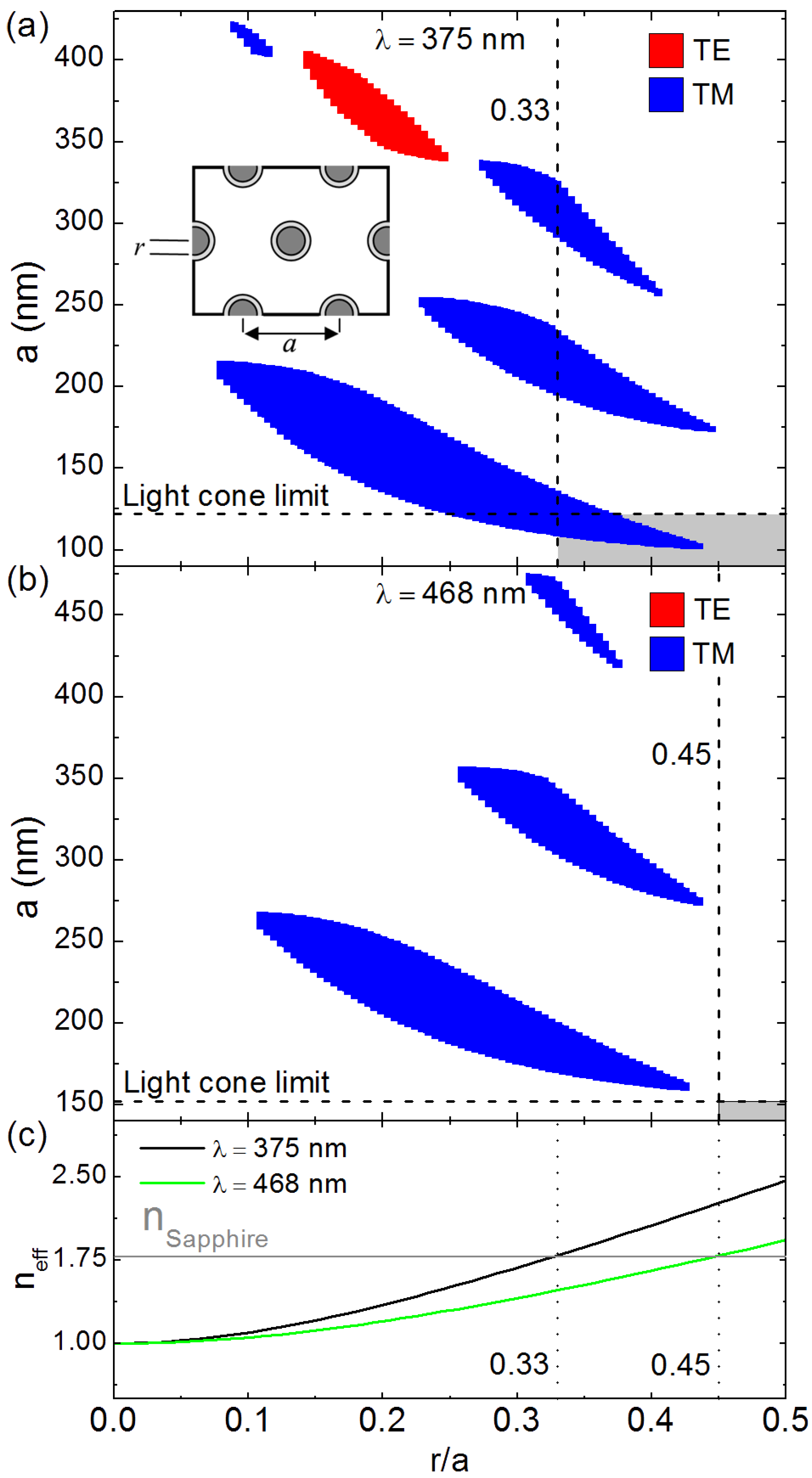
Figure 9.
(a) Photonic band-gap map of ZnO nanorods for λ = 375 nm; (b) Photonic band-gap map of ZnO nanorods for λ = 468 nm; (c) Effective refractive index of the ZnO nanorods obtained by Maxwell-Garnett approximation for λ = 375 nm and 468 nm.
Figure 9.
(a) Photonic band-gap map of ZnO nanorods for λ = 375 nm; (b) Photonic band-gap map of ZnO nanorods for λ = 468 nm; (c) Effective refractive index of the ZnO nanorods obtained by Maxwell-Garnett approximation for λ = 375 nm and 468 nm.
Figure 9a,b respectively show the PBG map calculated for a hexagonal lattice of ZnO nanorods at λ = 375 nm (ZnO excitonic emission) and λ = 468 nm (polymer emission) for the TE (red) and TM (blue) modes. As expected,
Figure 9a,b shows that ZnO nanorods have a preferably TM polarized band-gap. For λ = 375 nm,
Figure 9a shows the existence of several TM band-gap for
r/
a values ranging from 0.08 to 0.43 and a values ranging from 100 nm to 430 nm. In addition,
Figure 9a shows the existence of a TE bandgap for
r/
a values ranging from 0.15 to 0.25 and a values ranging from 337 nm to 404 nm. On the other hand, for λ = 468 nm,
Figure 9b shows only TM polarized bandgaps for
r/
a values ranging from 0.11 to 0.43 and a values ranging from 160 nm to 470 nm. The photonic gap map is an effective tool for the choice of the structure parameters
a and
r. However, other considerations must also be taken into account in order to make the best choice of structure parameters. For instance, photonic band-gaps only affect light that is guided within the structured layer (
i.e., ZnO nanorods). We recall that here we are dealing with ZnO nanostructures on sapphire. For such nanostructures, PBGs are only interesting if they lie under the limit
a/λ = 0.325 defined by the light cone between the ZnO structures and the sapphire substrate [
34]. For structures having
a/λ = 0.325, light begins leaking into the sapphire substrate. Therefore, structures with
a < 122 nm for λ = 375 nm and
a < 152 nm for λ = 468 nm would be most suitable for having a photonic band-gap effect. Another important issue is the effective refractive index. The nanostructured layer presents effective medium resulting from the mixture of air and ZnO. It is, therefore, essential for the nanostructured layer to have an effective refractive index greater than that of the sapphire substrate in order to support guided modes.
Figure 9c presents the evolution of the effective refractive index (
neff) obtained using Maxwell-Garnett approximation [
39,
40] for a hexagonal lattice of ZnO nanorods as a function of
r/
a. As expected,
Figure 9c shows that
neff increases with increasing
r/
a. Moreover,
Figure 9c shows that
neff is only greater than the refractive index of sapphire for
r/
a > 0.33 for λ = 375 nm and
r/
a > 0.45 for λ = 468 nm.
Figure 9a thus shows that the limits of the light cone and the effective refractive index at λ = 375 nm (
a < 122 nm and
r/
a > 0.33) are only verified by a narrow window of the first order TM-polarized PBG. Meanwhile,
Figure 9b shows no PBG verifying the light cone and effective refractive index limits at λ = 468 nm (
a < 152 nm and
r/
a > 0.45). It is important to stress that ZnO emission is mostly TE polarized [
33,
34]. Thus, for a PBG effect, perforated ZnO photonic crystal slabs would be more suitable than ZnO nanorods, as they present preferably TE polarized bandgaps [
20,
34]. Nevertheless, ZnO nanorods are more interesting for having high light extraction efficiency, due to their low effective refractive index. Moreover, ZnO nanorods would be more interesting for enlarging the sensing surface. ZnO nanorods present a more important specific surface (
Figure 6) compared to perforated ZnO thin films (
Figure 7).
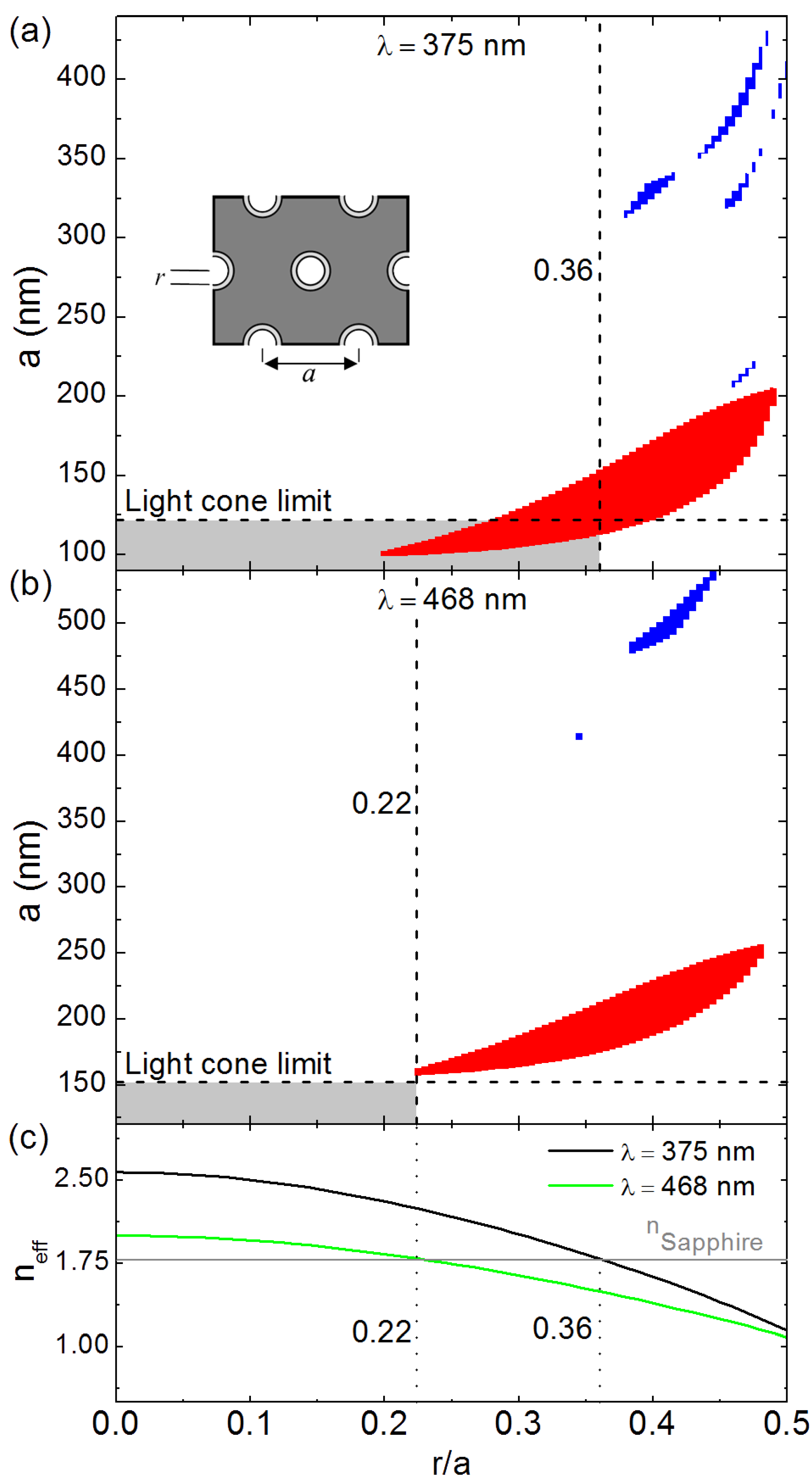
Similarly to
Figure 9,
Figure 10a,b respectively show the PBG map calculated for a hexagonal lattice of air nanoholes perforated in a ZnO slab at λ = 375 nm (ZnO excitonic emission) and λ = 468 nm (polymer emission) for the TE (red) and TM (blue) modes. As expected,
Figure 10a,b shows that the perforated ZnO slab has a preferably TE polarized band-gap. For λ = 375 nm,
Figure 10a shows the existence of TE band-gap for
r/
a values ranging from 0.2 to 0.49 and
a values ranging from 100 nm to 204 nm. In addition,
Figure 10 shows the existence of several TM bandgaps for
r/
a values ranging from 0.38 to 0.5 and
a values ranging from 200 nm to 430 nm. On the other hand, for λ = 468 nm,
Figure 10b shows TE polarized bandgap for
r/
a values ranging from 0.22 to 0.48 and
a values ranging from 160 nm to 256 nm.
Figure 10b also shows the existence of a TM polarized bandgap for
r/
a values ranging from 0.34 to 0.44 and
a values ranging from 415 nm to 540 nm. As previously mentioned, perforated ZnO slabs are most suitable for a pronounced photonic band gap effect on ZnO emission. We remind that
a < 122 nm for λ = 375 nm and
a < 152 nm for λ = 468 nm define the limits of the light cone between the ZnO slab and the sapphire substrate.
Figure 10c presents the evolution of the effective refractive index (
neff) obtained using Maxwell-Garnett approximation for a hexagonal lattice of air nanoholes perforated in ZnO slab as a function of
r/
a. As expected,
Figure 10c shows that
neff decreases with increasing
r/
a.
Figure 10c shows that
neff is only greater than the refractive index of sapphire for
r/
a < 0.36 for λ = 375 nm and
r/
a < 0.25 for λ = 468 nm.
Figure 10a thus shows that the limits of the light cone and the effective refractive index at λ = 375 nm (
a < 122 nm and
r/
a < 0.36) are only verified by a narrow window of the first order TE-polarized PBG. Meanwhile,
Figure 10b shows no PBG verifying the light cone and effective refractive index limits at λ = 468 nm (
a < 152 nm and
r/
a < 0.25). Structures which have
r/
a = 0.3 and
a = 116 nm should present interesting photonic band-gap properties.
Figure 10.
(a) Photonic band-gap map of perforated ZnO slab for λ = 375 nm; (b) Photonic band-gap map of perforated ZnO slab for λ = 468 nm; (c) Effective refractive index of the perforated ZnO slab obtained by Maxwell-Garnett approximation for λ = 375 nm and 468 nm.
Figure 10.
(a) Photonic band-gap map of perforated ZnO slab for λ = 375 nm; (b) Photonic band-gap map of perforated ZnO slab for λ = 468 nm; (c) Effective refractive index of the perforated ZnO slab obtained by Maxwell-Garnett approximation for λ = 375 nm and 468 nm.
Photonic band-gaps result from an ordered optical feedback occurring over a large scale. However, ZnO nanostructures, such as nanorods, can offer many photonic properties over a much smaller, even individual, scale. Such photonic properties can be extremely interesting for the fluorescence excitation of extremely thin polymer layers.
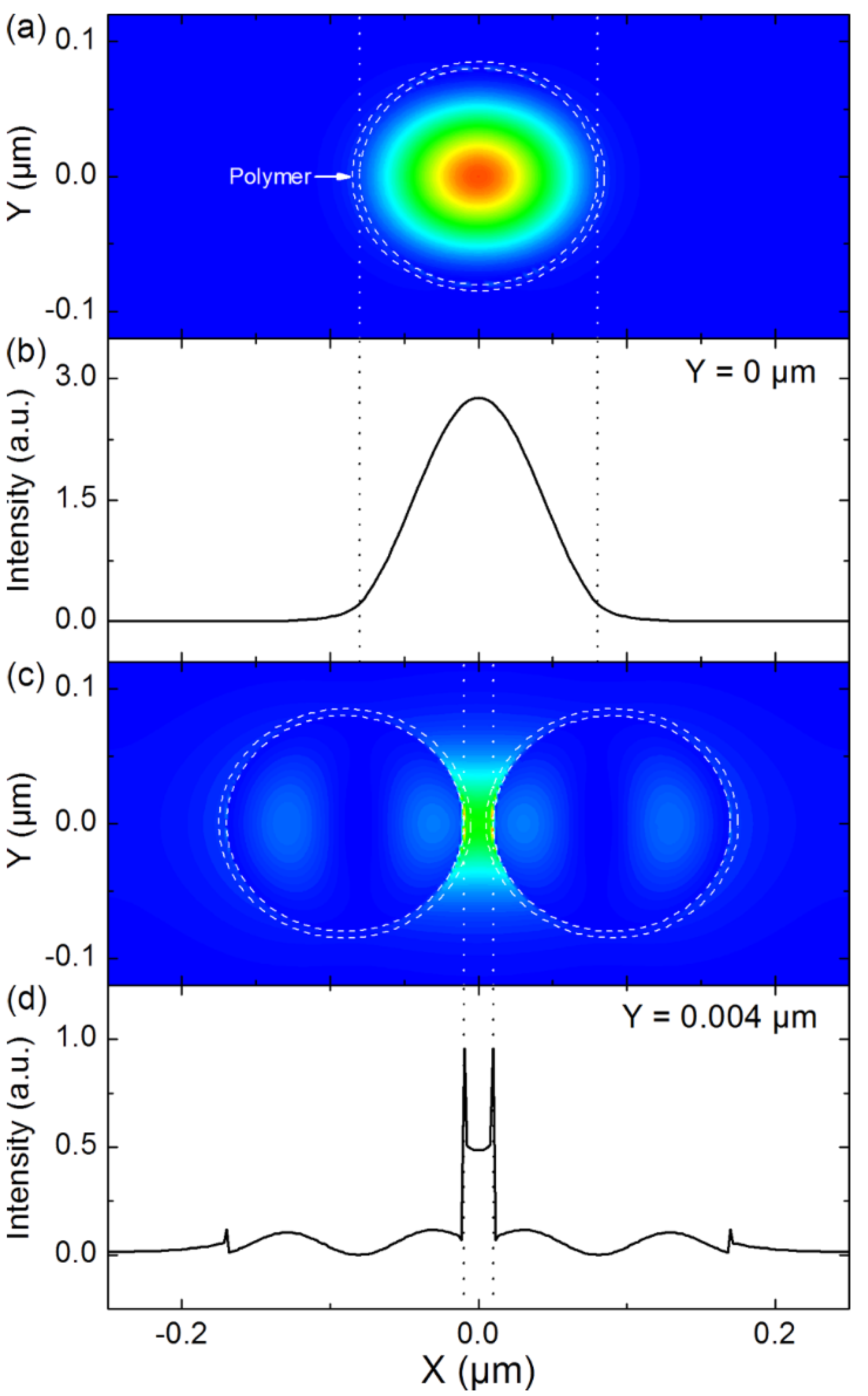
Figure 11 shows finite element method (FEM) results for a ZnO nanorod (
Figure 11a,b) and two coupled ZnO nanorods (
Figure 11c,d). The FEM calculations were realized at λ = 375 nm. For the two structures, the ZnO nanorods has a diameter of 160 nm. The two coupled ZnO nanorods are separated by a 20 nm air gap.
Figure 11a shows the Poynting vector amplitude distribution of the guided mode in the ZnO nanorod. As seen is
Figure 11a, a ZnO nanorod can support guided modes even at a nanometric scale.
Figure 11b shows an X-Cut of the guided mode profile at the middle of the ZnO nanorod (
i.e.,
Y = 0 µm). As expected,
Figure 11b shows that the guided mode has a Gaussian profile. The guided mode is highly confined inside the ZnO nanorod. Only a small part of the evanescent tail, sticks out of the ZnO nanorod.
Figure 11c shows the Poynting vector amplitude distribution of the gap mode for the coupled ZnO nanorods. As seen in
Figure 11c, the energy of the gap mode is confined within the 20 nm air gap in between the two ZnO nanorods.
Figure 11d shows a X-cut of the gap mode profile slight above the middle of the two nanorods (at
Y = 0.004 µm).
Figure 11d reveals the existence of a sharp peak at the edge of each ZnO nanorod.
Figure 11d thus shows that the energy of the gap mode is strongly confined at the air/ZnO interface. The dashed circles in
Figure 11a,c defines the limits of the area that would occupy a 5 nm thick polymer coated on the ZnO nanorods. For the polymer fluorescence excitation, two quantities are to be considered, the excitation intensity over the whole polymer area and the excitation intensity at a local scale. The excitation intensity over the whole polymer area for
Figure 11c (
i.e., the coupled ZnO nanorods) is almost 2 times higher than that of
Figure 11a (
i.e., the single ZnO nanorod). The gap mode can thus lead to a two-fold enhancement in the polymer fluorescence. Compared to the guided mode (
Figure 11a), the gap mode (
Figure 11c) is confinement within a much smaller surface. The local excitation intensity of the gap mode in the polymer layer (
Figure 11d) can reach up to 4–5 times that of the guided mode. Such high local intensities can be extremely beneficial for polymer layers exhibiting ASE, as they can lead to a drastic decrease of the lasing threshold. Such gap modes can be manifested in densely stacked randomly ordered ZnO nanorods.
To summarize, nanostructured ZnO offers a multitude of possible choices to enhance the signal of nanothin fluorescence sensing polymers. Random arrays of ZnO nanostructures, such as densely stacked ZnO nanowires with high aspect ratio, have a very large sensing surface and can exhibit strongly confined gap modes within the polymer volume, which can lead to a drastic enhancement in polymer fluorescence. Ordered arrays of ZnO nanostructures, on the other hand, offer the advantage of having a photonic bandgap. The photonic bandgap of perforated ZnO thin films is most appropriate for such purposes, as ZnO emission is preferable TE polarized. Perforated ZnO thin films exhibit lower lasing threshold, which can lead to a more efficient G-WET effect and therefore a better fluorescence excitation. It is evident that the use of ZnO nanostructures can most certainly lead to a drastic enhancement in the polymer fluorescence. However, at this level, it is hard to estimate, the enhancement factors that the various ZnO nanostructures would present, as the behavior of the polymer fluorescence towards the various photonic phenomena in act is still not deeply understood. Both experimental and theoretical (such as active FDTD) investigations are thus needed in order to determine the enhancement factors and to further understand the impact that each effect has on the polymer fluorescence.
Figure 11.
(a) Contour map of the Poynting vector amplitude distribution for the guided mode in a ZnO nanorod (defined by the inner dashed circle) with a diameter of 160 nm; (b) X-cut at Y = 0 µm for the guided mode profile for the ZnO nanorod; (c) Contour map of the Poyting vector amplitude distribution for the gap mode for 2 coupled ZnO nanorods (defined by the inner dashed circles). The coupled nanorods have a diameter of 160 nm and are separated by a 20 nm air gap; (d) X-cut at Y = 0.004 µm for the gap mode profile for the coupled ZnO nanorods.


