
Transient Photocurrent Response of Plasmon-Enhanced Polymer Solar Cells with Gold Nanoparticles

Abstract
:1. Introduction
2. Experimental
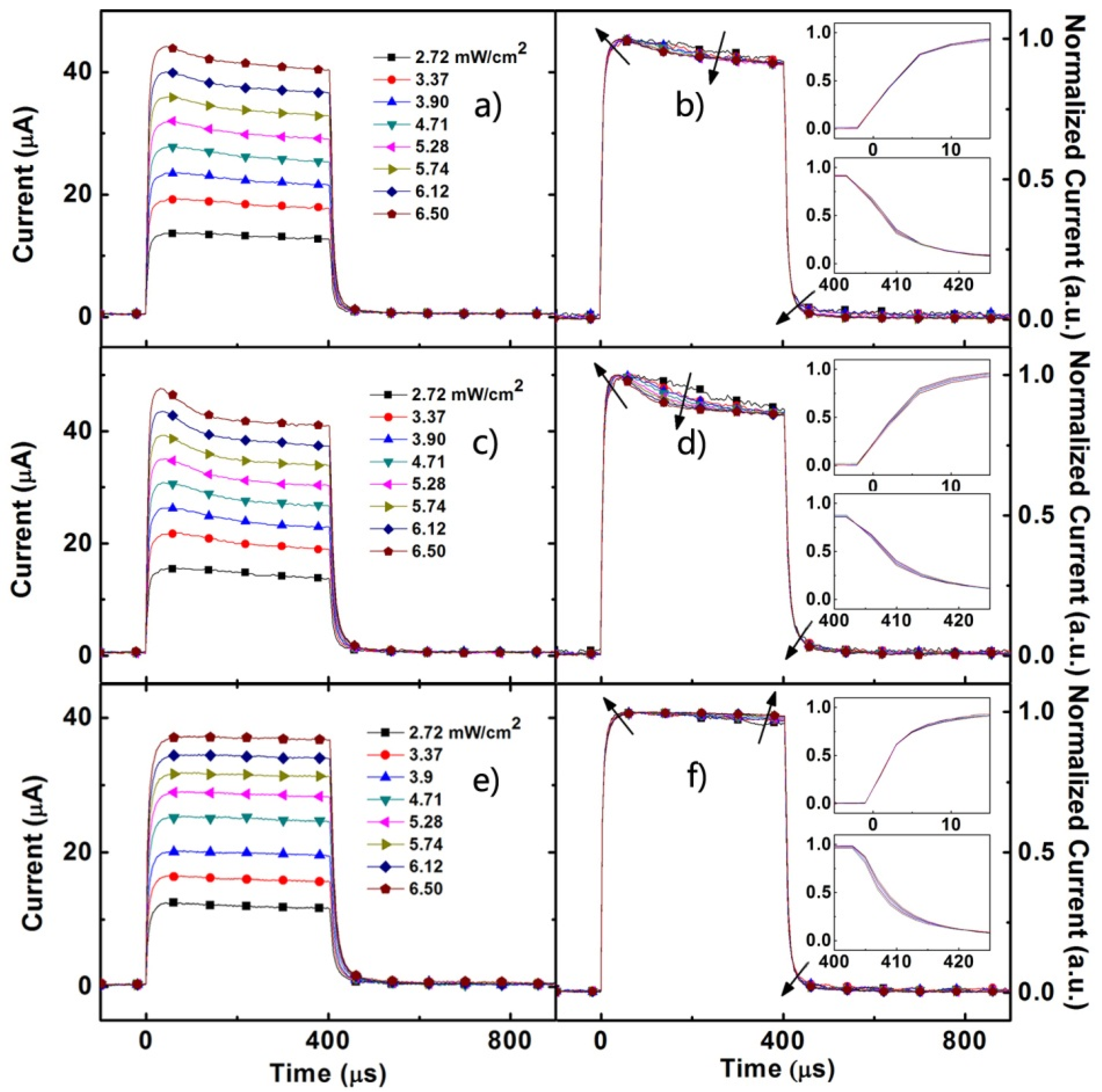
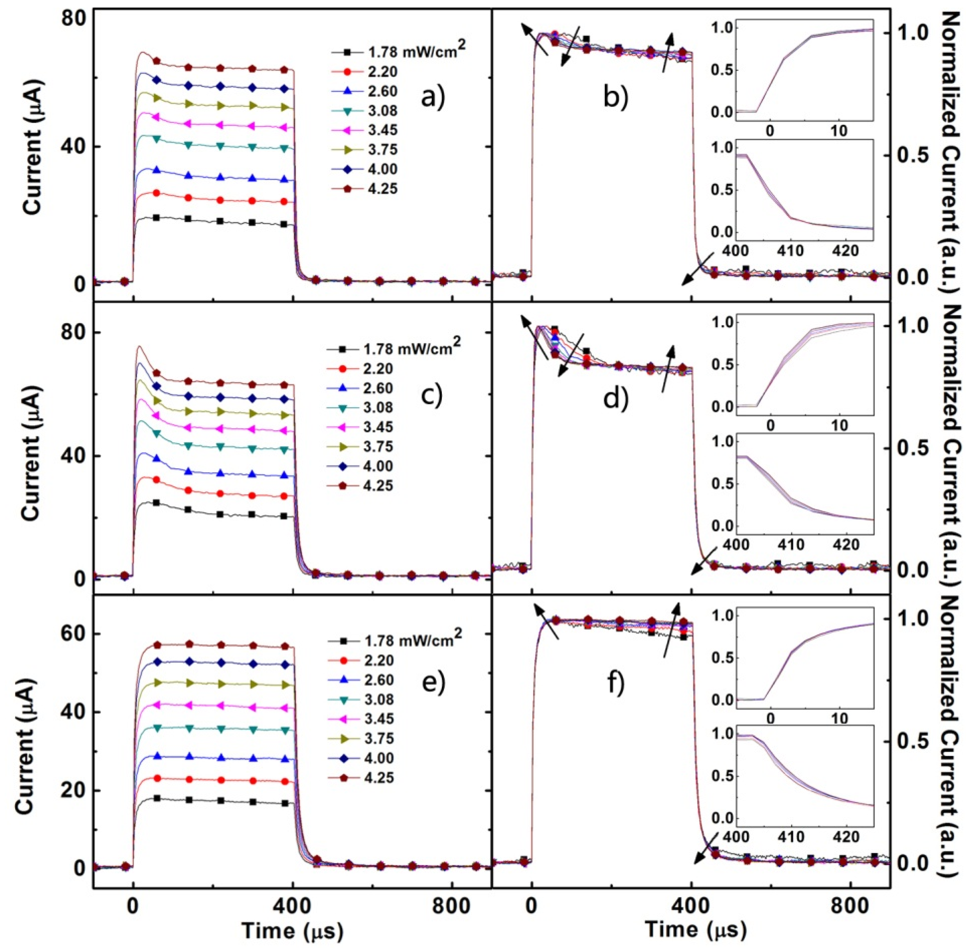
3. Discussion


| Devices | JSC (mA/cm2) | VOC (V) | Fill factor | PCE (%) |
|---|---|---|---|---|
| Device A | 8.18 | 0.62 | 0.58 | 2.93 |
| Device B | 8.50 | 0.62 | 0.57 | 2.98 |
| Device C | 7.63 | 0.62 | 0.56 | 2.64 |


4. Conclusions
Acknowledgments
Author Contributions
Conflicts of Interest
References
- Kippelen, B.; Bredas, J.L. Organic photovoltaics. Energy Environ. Sci. 2009, 2, 251–261. [Google Scholar] [CrossRef]
- Helgesen, M.; Sondergaard, R.; Krebs, F.C. Advanced materials and processes for polymer solar cell devices. J. Mater. Chem. 2010, 20, 36–60. [Google Scholar] [CrossRef]
- You, J.; Dou, L.; Yoshimura, K.; Kato, T.; Ohya, K.; Moriarty, T.; Emery, K.; Chen, C.-C.; Gao, J.; Li, G.; et al. A polymer tandem solar cell with 10.6% power conversion efficiency. Nat. Commun. 2013, 4, 1446–1455. [Google Scholar] [CrossRef] [PubMed]
- He, Z.C.; Zhong, C.M.; Huang, X.; Wong, W.Y.; Wu, H.B.; Chen, L.W.; Su, S.J.; Cao, Y. Simultaneous enhancement of open-circuit voltage, short-circuit current density, and fill factor in polymer solar cells. Adv. Mater. 2011, 23, 4636–4643. [Google Scholar] [CrossRef] [PubMed]
- Shim, J.W.; Zhou, Y.; Fuentes-Hernandez, C.; Dindar, A.; Guan, Z.; Cheun, H.; Kahn, A.; Kippelen, B. Studies of the optimization of recombination layers for inverted tandem polymer solar cells. Sol. Energy Mater. Sol. Cells 2012, 107, 51–55. [Google Scholar] [CrossRef]
- Liang, Y.; Xu, Z.; Xia, J.; Tsai, S.-T.; Wu, Y.; Li, G.; Ray, C.; Yu, L. For the bright future-bulk heterojunction polymer solar cells with power conversion efficiency of 7.4%. Adv. Mater. 2010, 22, E135–E138. [Google Scholar] [CrossRef] [PubMed]
- Zou, Y.P.; Najari, A.; Berrouard, P.; Beaupré, S.; Aïch, B.R. A Thieno[3,4-c]pyrrole-4,6-dione-Based Copolymer for Efficient Solar Cells. J. Am. Chem. Soc. 2010, 132, 5330–5331. [Google Scholar] [CrossRef] [PubMed]
- Gilot, J.; Barbu, I.; Wienk, M.M.; Janssen, R.A.J. The use of ZnO as optical spacer in polymer solar cells: Theoretical and experimental study. Appl. Phys. Lett. 2007, 91, 113520–113522. [Google Scholar] [CrossRef]
- Gilot, J.; Wienk, M.M.; Janssen, R.A.J. Optimizing polymer tandem solar cells. Adv. Mater. 2010, 22, E67–E71. [Google Scholar] [CrossRef] [PubMed]
- Sista, S.; Park, M.-H.; Hong, Z.R.; Wu, Y.; Hou, J.H.; Kwan, W.L.; Li, G.; Yang, Y. Highly Efficient Tandem Polymer Photovoltaic Cells. Adv. Mater. 2010, 22, 380–383. [Google Scholar] [CrossRef] [PubMed]
- Pillai, S.; Green, M.A. Plasmonics for photovoltaic applications. Sol. Energy Mater. Sol. Cells 2010, 94, 1481–1486. [Google Scholar] [CrossRef]
- Dionne, J.A.; Sweatlock, L.A.; Atwater, H.A.; Polman, A. Planar metal plasmon waveguides: Frequency-dependent dispersion, propagation, localization, and loss beyond the free electron model. Phys. Rev. B 2005, 72. [Google Scholar] [CrossRef]
- Catchpole, K.R.; Polman, A. Design principles for particle plasmon enhanced solar cells. Appl. Phys. Lett. 2008, 93. [Google Scholar] [CrossRef]
- Chou, C.H.; Chen, F.C. Plasmonic nanostructures for light trapping in organic photovoltaic devices. Nanoscale 2014, 6, 8444–8458. [Google Scholar] [CrossRef] [PubMed]
- Yang, J.; You, J.; Chen, C.-C.; Hsu, W.-C.; Tan, H.; Zhang, X.W.; Hong, Z.; Yang, Y. Plasmonic Polymer Tandem Solar Cell. ACS Nano 2011, 5, 6210–6217. [Google Scholar] [CrossRef] [PubMed]
- Stavytska-Barba, M.; Salvador, M.; Kulkarni, A.; Ginger, D.S.; Kelley, A.M. Plasmonic Enhancement of Raman Scattering from the Organic Solar Cell Material P3HT/PCBM by Triangular Silver Nanoprisms. J. Phys. Chem. C 2011, 115, 20788–20794. [Google Scholar] [CrossRef]
- Qiao, L.; Wang, D.; Zuo, L.; Ye, Y.; Qian, J.; Chen, H.; He, S. Localized surface plasmon resonance enhanced organic solar cell with gold nanospheres. Appl. Energy 2011, 88, 848–852. [Google Scholar] [CrossRef]
- Heo, M.; Cho, H.; Jung, J.-W.; Jeong, J.-R.; Park, S.; Kim, J.Y. High-Performance Organic Optoelectronic Devices Enhanced by Surface Plasmon Resonance. Adv. Mater. 2011, 23. [Google Scholar] [CrossRef] [PubMed]
- Wang, D.H.; Park, K.H.; Seo, J.H.; Seifter, J.; Jeon, J.H.; Kim, J.K.; Park, J.H.; Park, O.O.; Heeger, A.J. Enhanced Power Conversion Efficiency in PCDTBT/PC70BM Bulk Heterojunction Photovoltaic Devices with Embedded Silver Nanoparticle Clusters. Adv. Energy Mater. 2011, 5, 766–770. [Google Scholar] [CrossRef]
- Xie, F.X.; Choy, W.C.H.; Wang, C.C.D.; Sha, W.E.I.; Fung, D.D.S. Improving the efficiency of polymer solar cells by incorporating gold nanoparticles into all polymer layers. Appl. Phys. Lett. 2011, 99. [Google Scholar] [CrossRef] [Green Version]
- Wu, J.-L.; Chen, F.-C.; Hsiao, Y.-S.; Chien, F.-C.; Chen, P.; Kuo, C.-H.; Huang, M.H.; Hsu, C.-S. Surface Plasmonic Effects of Metallic Nanoparticles on the Performance of Polymer Bulk Heterojunction Solar Cells. ACS Nano 2011, 5, 959–967. [Google Scholar] [CrossRef] [PubMed]
- Wang, D.H.; Kim, D.Y.; Choi, K.W.; Seo, J.H.; Im, S.H.; Park, J.H.; Park, O.O.; Heeger, A.J. Enhancement of Donor-Acceptor Polymer Bulk Heterojunction Solar Cell Power Conversion Efficiencies by Addition of Au Nanoparticles. Angew. Chem. Int. Ed. 2011, 50, 5519–5523. [Google Scholar] [CrossRef] [PubMed]
- Jung, K.; Song, H.-J.; Lee, G.; Ko, Y.; Ahn, K.J.; Choi, H.; Kim, J.Y.; Ha, K.; Song, J.; Lee, J.-K.; et al. Plasmonic Organic Solar Cells Employing Nanobump Assembly via Aerosol-Derived Nanoparticles. ACS Nano 2014, 8, 2590–2601. [Google Scholar] [CrossRef] [PubMed]
- Chuang, M.-K.; Lin, S.-W.; Chen, F.-C.; Chub, C.-W.; Hsuc, C.-S. Gold nanoparticle-decorated graphene oxides for plasmonic-enhanced polymer photovoltaic devices. Nanoscale 2014, 6, 1573–1579. [Google Scholar] [CrossRef] [PubMed]
- McNeill, C.R.; Hwang, I.; Greenham, N.C. Photocurrent transients in all-polymer solar cells: Trapping and detrapping effects. J. Appl. Phys. 2009, 106. [Google Scholar] [CrossRef]
- Mihailetchi, V.D.; Wildeman, J.; Blom, P.W.M. Space-Charge Limited Photocurrent. Phys. Rev. Lett. 2005, 94. [Google Scholar] [CrossRef]
- Perez-Juste, J.; Pastoriza-Santos, I.; Liz-Marzan, L.M.; Mulvaney, P. Gold nanorods: Synthesis, characterization and applications. Coord. Chem. Rev. 2005, 249, 1870–1901. [Google Scholar] [CrossRef]
- Seo, S.S.; Wang, X.H.; Murray, D. Direct monitoring of gold nanorod growth. Ionics 2009, 15, 67–71. [Google Scholar] [CrossRef]
- Jägeler-Hoheisel, T.; Selzer, F.; Riede, M.; Leo, K. Direct Electrical Evidence of Plasmonic Near-Field Enhancement in Small Molecule Organic Solar Cells. J. Phys. Chem. C 2014, 118, 15128–15135. [Google Scholar] [CrossRef]
- Fang, Y.; Hou, Y.; Lou, Z.; Teng, F.; Tang, A.; Hu, Y. Surface plasmonic effect and scattering effect of Au nanorods on the performance of polymer bulk heterojunction solar cells. Sci. China Technol. Sci. 2013, 56, 1865–1869. [Google Scholar] [CrossRef]
- Lee, J.H.; Park, J.H.; Kim, J.S.; Lee, D.Y.; Cho, K. High efficiency polymer solar cells with wet deposited plasmonic gold nanodots. Organ. Electron. 2009, 10, 416–420. [Google Scholar] [CrossRef]
- Shuttle, C.G.; Hamilton, R.; Nelson, J.; O’Regan, B.C.; Durrant, J.R. Measurement of Charge-Density Dependence of Carrier Mobility in an Organic Semiconductor Blend. Adv. Funct. Mater. 2010, 20, 698–702. [Google Scholar] [CrossRef]
- Li, Z.; McNeill, C.R. Transient photocurrent measurements of PCDTBT:PC70BM and PCPDTBT:PC70BM Solar Cells: Evidence for charge trapping in efficient polymer/fullerene blends. J. Appl. Phys. 2011, 109. [Google Scholar] [CrossRef]
- Hwang, I.; McNeill, C.R.; Greenham, N.C. Drift-diffusion modeling of photocurrent transients in bulk heterojunction solar cells. J. Appl. Phys. 2009, 106. [Google Scholar] [CrossRef]
- Li, Z.; Gao, F.; Greenham, N.C.; McNeill, C.R. Comparison of the Operation of Polymer/Fullerene, Polymer/Polymer, and Polymer/Nanocrystal Solar Cells: A Transient Photocurrent and Photovoltage Study. Adv. Funct. Mater. 2011, 21, 1419–1431. [Google Scholar] [CrossRef]
- Ginger, D.S.; Greenham, N.C. Charge injection and transport in films of CdSe nanocrystals. J. Appl. Phys. 2000, 87. [Google Scholar] [CrossRef]
- Lifshitz, E.; Dag, I.; Litvitn, I.D. Optically Detected Magnetic Resonance Study of Electron/Hole Traps on CdSe Quantum Dot Surfaces. J. Phys. Chem. B 1998, 102, 9245–9250. [Google Scholar] [CrossRef]
© 2015 by the authors; licensee MDPI, Basel, Switzerland. This article is an open access article distributed under the terms and conditions of the Creative Commons Attribution license (http://creativecommons.org/licenses/by/4.0/).
Share and Cite
Fang, Y.; Hou, Y.; Hu, Y.; Teng, F. Transient Photocurrent Response of Plasmon-Enhanced Polymer Solar Cells with Gold Nanoparticles. Materials 2015, 8, 4050-4060. https://doi.org/10.3390/ma8074050
Fang Y, Hou Y, Hu Y, Teng F. Transient Photocurrent Response of Plasmon-Enhanced Polymer Solar Cells with Gold Nanoparticles. Materials. 2015; 8(7):4050-4060. https://doi.org/10.3390/ma8074050
Chicago/Turabian StyleFang, Yi, Yanbing Hou, Yufeng Hu, and Feng Teng. 2015. "Transient Photocurrent Response of Plasmon-Enhanced Polymer Solar Cells with Gold Nanoparticles" Materials 8, no. 7: 4050-4060. https://doi.org/10.3390/ma8074050