1. Introduction
Microfluidic devices have become key tools in many fields, including analytical chemistry, life sciences, and medicine, in conjunction with the ongoing development and increased utilization of labs-on-a-chip and micro total analysis systems (µTAS) [
1,
2,
3,
4,
5]. This growth has primarily been based on various novel fabrication techniques [
6,
7,
8] for downsizing and integrating all of the micro/nanocomponents necessary for a given function, such as a reaction or analysis. These components include both fluid-control elements (pumps, valves, etc.) and functional elements (heaters, separation structures, and so on). Bioanalytical devices for DNA sequencing and protein analysis were the first major application of microfluidic devices [
9,
10,
11,
12], but these devices have been rapidly adopted in other scientific areas, especially in collaborations between medicine and engineering [
13]. The current trend is growth in point-of-care, personalized medicine and medical implant devices, and an expanding range of component materials [
8,
14,
15].
In this context, basic studies regarding microprocessing technologies and materials that will enable effective fabrication of three-dimensional (3D) microchannel structures are required to improve the performance, functionality, and packing density of these devices [
5,
16,
17,
18,
19]. In some cases, two-dimensional microchannels have been patterned on substrates made of glass or polymeric materials, including heat-curable silicone elastomers. These substrates are typically laminated together to obtain the desired three-dimensional structures. However, lamination is insufficient to satisfy the requirements of all three-dimensional structures because the extensibility of such structures is limited to the direction parallel to the substrate surface.
Recently, it has been reported that 3D channel structures can be rapidly fabricated using 3D printers, which have become popular as they represent convenient manufacturing tools. Additionally, the specific functions of microfluidic systems can be easily expanded based on both the lamination of two-dimensional microfabricated substrates and the assembly of 3D parts made of more than one material. Examples include transparent microchannels made of glass to allow for observations, high conductivity surfaces made of metals and acting as electrodes, and flexible structures made of silicone. Despite these advantages, fluid leaks originating at the joints between rough surfaces remain a critical problem associated with microfluidic devices composed of several parts and with imprecise structures.
In the present study, we developed and investigated a novel fabrication technique to address this challenge. A paraffin-based polymer and a photo-curable silicone elastomer were employed to fabricate a liquid-tight microchannel on a rough surface, with the paraffin polymer serving as a mold for the microchannel, which was made of silicone elastomer. The shape transfer capability of the paraffin polymer mold was assessed by evaluating the surface roughness of the finished product. Additionally, the performance of the liquid-tight microchannel between the microchannel substrate made of silicone elastomer and the bottom substrate made of acrylonitrile butadiene styrene resin (ABS) resin was verified with a demonstration of electrophoresis in the microchannel.
2. Materials and Methods
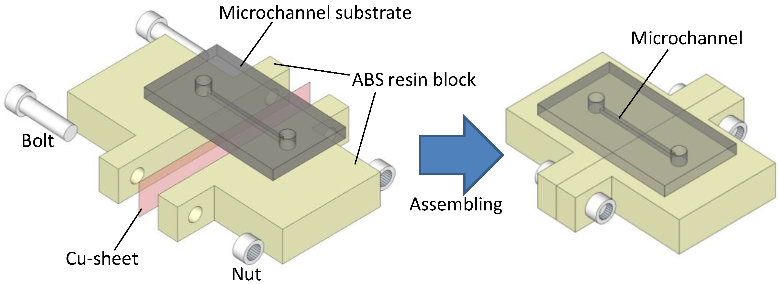
To verify the proposed fabrication technique, we demonstrated electrophoresis in a microfluidic device made by the technique shown in
Figure 1. This device incorporated a straight microchannel with a height of 90 µm, a width of 500 µm and a length of 3 mm. The lower surface of the channel was composed of two ABS resin blocks, each 30 × 30 × 5 mm
3 and fabricated using a 3D printer (Mojo 3D printer, Stratasys Inc., Eden Prairie, MN, USA). A 50-µm-thick copper sheet was used as the electrode during electrophoresis, sandwiched tightly between the blocks using two nuts and two bolts.
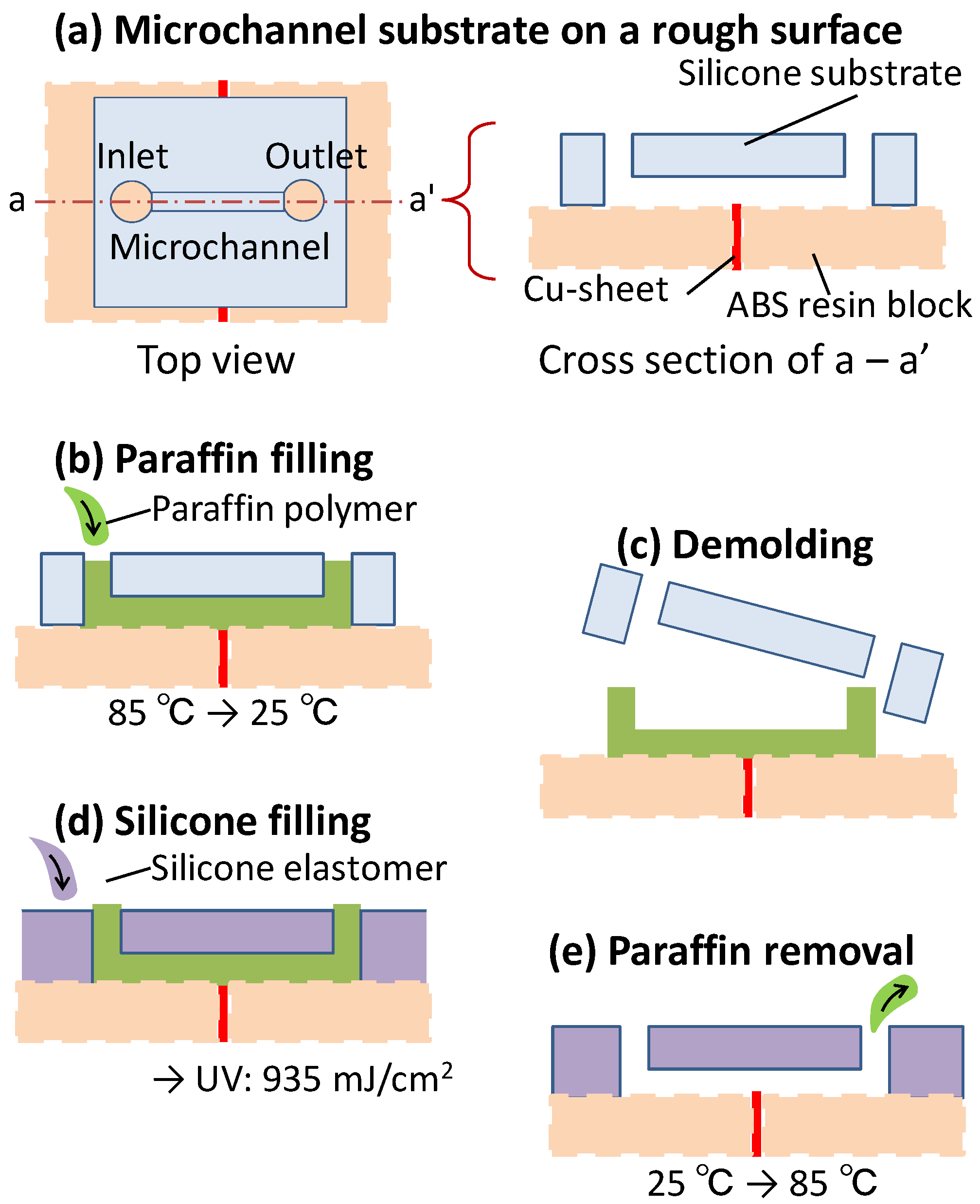
Figure 2 summarizes the proposed technique for the creation of a liquid-tight microchannel. The initial microchannel structure on the silicone substrate is made using a conventional lithography technique [
20]. Although the structure on the substrate is typically employed directly as the microchannel, it is important to consider the possibility of liquid leaks in the case that the bottom substrate contains joints between various parts or exhibits significant roughness (
Figure 2a).
In the first step of the proposed technique, a paraffin polymer (Hayashi Pure Chemical Ind. Co., Ltd., Osaka, Japan) is heated to 85 °C and injected into the microchannel mold, which is sealed at its base by the bottom substrate, as shown in
Figure 2b. A key point here is that the microchannel mold must be held down tightly on the substrate using a rubber band prior to injecting the paraffin. After cooling the paraffin polymer to room temperature, the microchannel substrate is peeled away from the substrate as in
Figure 2c. The microchannel structure is now transferred to the paraffin polymer on the substrate used to help form the microchannel, even if the substrate includes joints or has significant roughness. As shown in
Figure 2d, the photo-curable silicone elastomer (X-34-4184, Shin-Etsu Silicone, Tokyo, Japan) is then cast into the mold to seal any possible spaces that could result in leaks along the bottom substrate. This elastomer is subsequently cured without the application of high temperature, by UV light irradiation at an energy of 0.94 J/cm
2, using a low-pressure mercury lamp (Multilight: ML-251, Ushio Inc., Tokyo, Japan) equipped with a 365 nm wavelength bandpass filter [
21]. This low temperature fabrication process maintains the shape of the microchannel structure formed by the low melting point paraffin polymer. Additionally, gaps between the elastomer and the bottom surface caused by distortion of the elastomer are avoided owing to the unique low-shrinkage characteristics of the elastomer. Following 30 min of light exposure, the paraffin polymer in the microchannel is removed by heating the apparatus to 85 °C (
Figure 2e).
3. Experimental Section
To verify the applicability of the proposed technique for microfabrication, the shape transfer capability of the fabricated microchannel was evaluated as an indicator of the accuracy of this process. This was accomplished by assessing the shape and roughness of the paraffin polymer mold and the channel using laser microscopy (VK-X210, Keyence, Osaka, Japan).
Additionally, to estimate the sealing performance of the fabricated microchannel, we performed the electrophoresis of a fluorescent molecule (fluorescein, F1300, Molecular Probes, Inc., Eugene, OR, USA) dissolved in distilled water at 10 µg/mL. The fluorescent emission of the fluorescein, as assessed using a fluorescent microscopy system (Microscope: IX 73, Olympus, Tokyo, Japan; Camera: DP72, Olympus), was used to visualize leakage of the solution from the microchannel. During these leak tests, the fluorescein solution was injected into the microchannel at a rate of 10 mL/min via a syringe pump (Kd Scientific, Holliston, MA, USA) and a voltage of 20 V was applied to initiate electrophoresis. The negative terminal of an electronic power supply (P4K-80M, Matsusada, Shiga, Japan) was connected to the copper sheet of the device, while the positive terminal was connected to a wire placed in the outlet of the channel, as shown in
Figure 3.
4. Results and Discussion
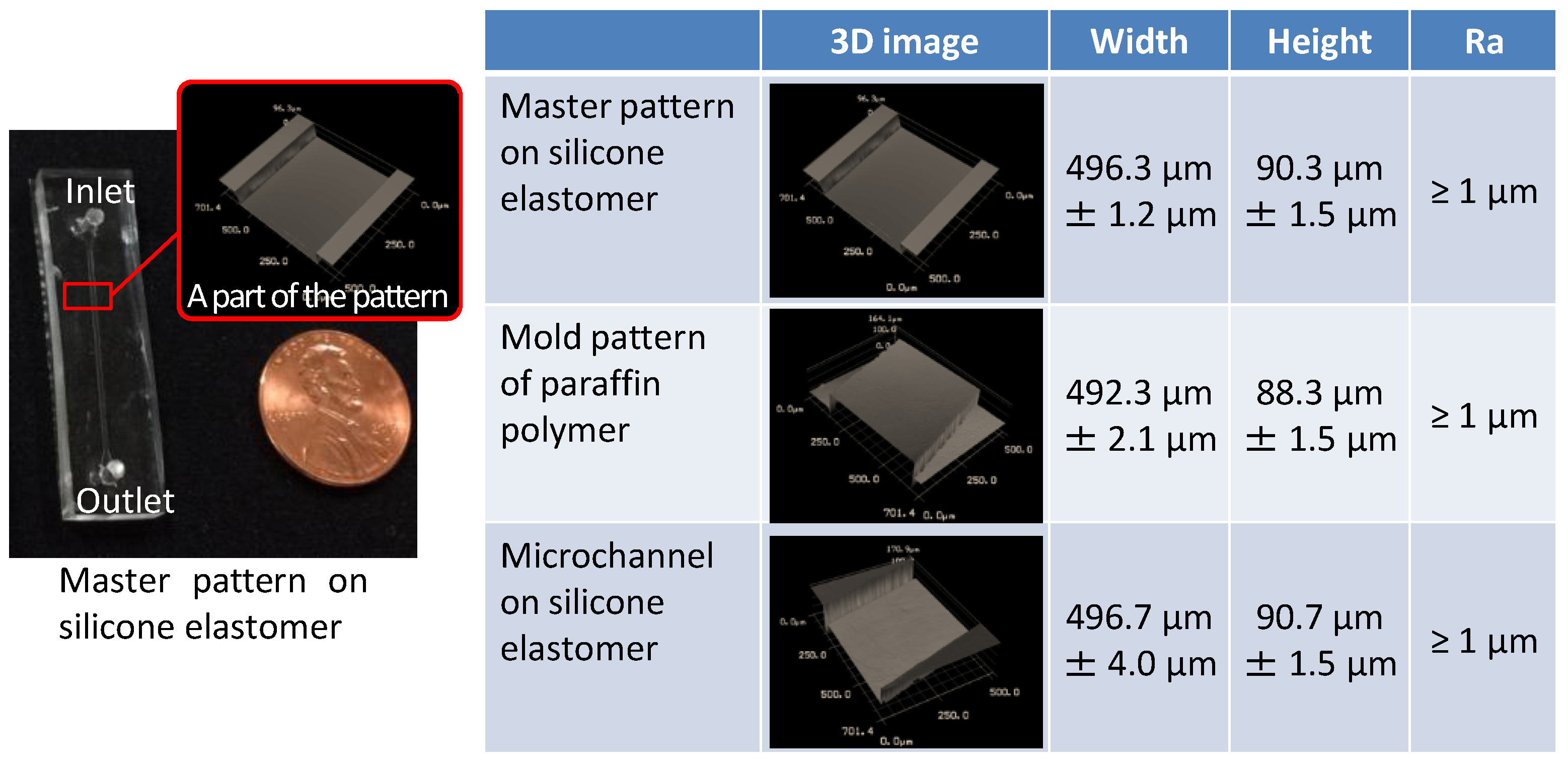
Figure 4 shows microscopy images of the channel structure fabricated by the proposed technique, applying a master pattern with a width of 496.3 µm and a height of 90.3 µm. Although the dimensions of the molded paraffin presented in this figure are 0.8%–2.2% smaller than the master pattern, the completed microchannel on the silicone elastomer was in good agreement with the master pattern, and the difference is 0.1%–0.4%. It is therefore likely that the apparent difference in the paraffin pattern dimensions was simply a measurement error.
The arithmetic average of the roughness (Ra) over a 300 × 300 µm2 region of each of these patterns was less than 1 µm, which was the minimum value of roughness resolution in the measurement system employed. Although we consider that additional evaluation depending on the intended application will be necessary in future, the roughness resolution obtained in the present study was sufficient for the purposes of our demonstration. These results indicate that the master pattern was successfully transferred to the paraffin polymer and subsequently to the silicone elastomer, the dimensions of which were in good agreement with those of the master pattern.
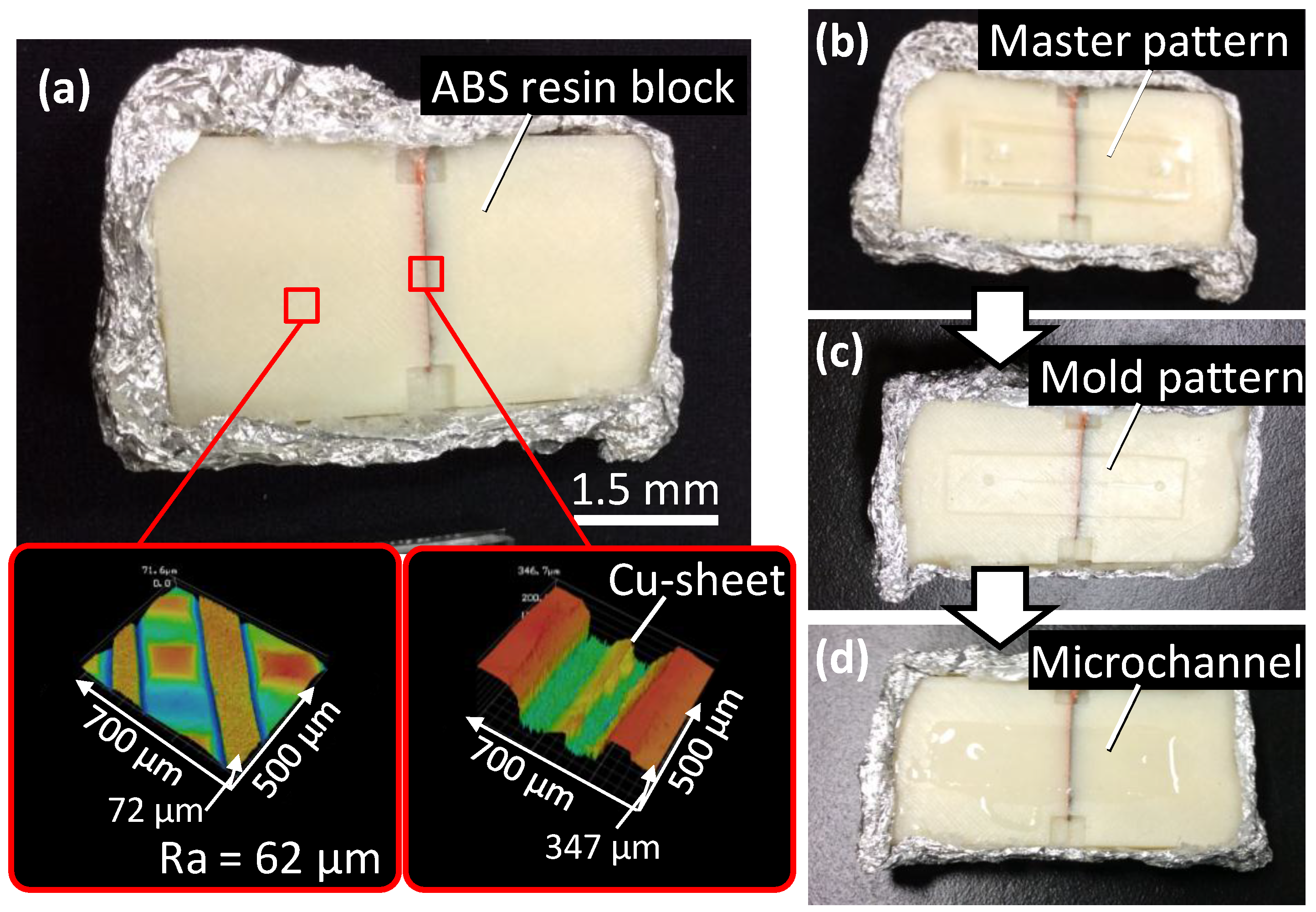
Figure 5 presents images of the actual substrates during this process.
Figure 5a shows the bottom substrate, composed of a copper sheet and an ABS resin block, the surface of which had a net-like morphology with a
Ra of 62 µm over a 1.4 × 1.1 mm
2 area. The gap at the joint between the copper sheet and the resin block was 175 µm wide and 219 µm deep. The master pattern on the bottom substrate was transferred to the silicone elastomer through the molded pattern of the paraffin polymer, as shown in
Figure 5b–d.
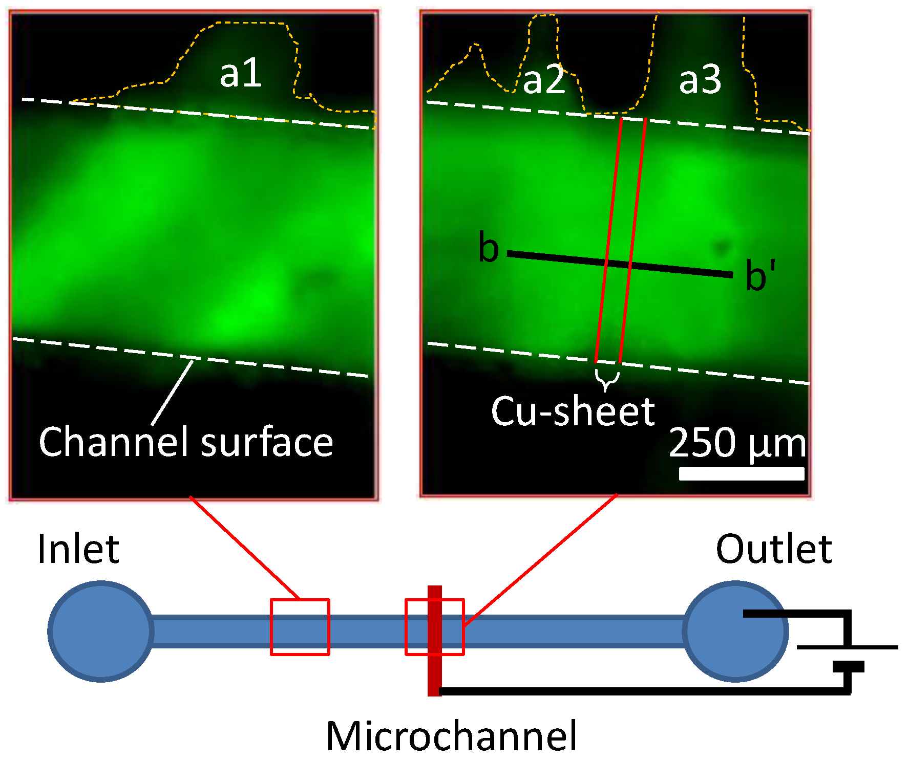
Electrophoresis was demonstrated utilizing the microchannel of the fabricated device. In the case of a microchannel substrate made using a conventional technique, it would be impossible to confirm any structures, including the boundaries of the microchannel, because the significant roughness of the bottom substrate would have resulted in leaks of the injected solution. In the present device, however, the fluorescent image of the fluorescein in the microchannel clearly indicated the boundary of the channel surface in the microchannel made by this new technique, as shown in
Figure 6. In these images, the variable intensity in the microchannel indicates a difference in depth resulting from the roughness of the bottom substrate. Although a small amount of fluorescein was confirmed to have leaked to the exterior of the channel (as indicated at the sites labeled a1, a2 and a3 in
Figure 6), the fluorescent intensity and apparent flow of the fluorescein in the microchannel demonstrate that there was negligible dead end space.
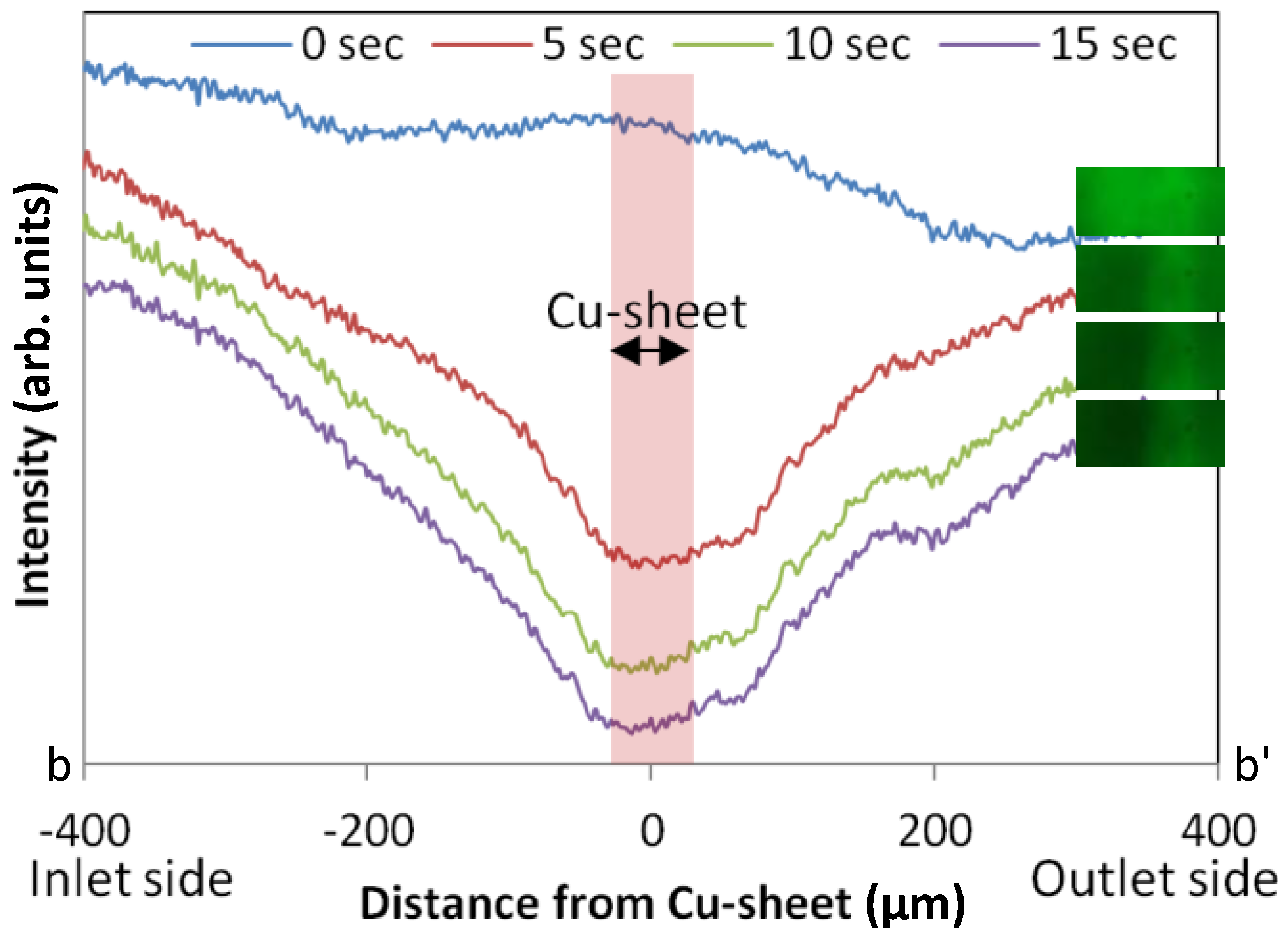
Figure 7 presents the result of the electrophoresis of fluorescein in the microchannel. The change in the signal intensity, which was obtained by subtracting a background, was measured for 15 s after applying a voltage to the line between b and b’ indicated in
Figure 6. Over the first 5 s, the intensity rapidly decreased in the vicinity of the copper sheet due to electrophoresis. It is evident from this result that the proposed technique has the potential to fabricate unique structures using several different materials for various applications.
5. Conclusions
As a means of improving the 3D construction of microfluidic devices, we developed a novel technique for fabricating liquid-tight microchannels between two different device components. Using this method, a microchannel was formed using a photo-curable silicone polymer and was tightly sealed against a bottom substrate which had both joined parts and significant roughness. From measurements of the microchannel dimensions and the roughness of the transferred structure, it was evident that the master pattern was successfully transferred first to the paraffin polymer with a 0.8%–2.2% difference and then to the silicone elastomer with a 0.1%–0.4% difference, which was in good agreement with the dimensions of the master pattern. A liquid-tight microchannel of photo-curable silicone was successfully fabricated on this very rough substrate (Ra = 62 µm). As the operation example of a microfluidic device which has a three-dimensional structure composed of several parts such as an electrode of copper, a bottom substrate of ABS resin and a microchannel of silicone, an experiment of electrophoresis in the microchannel was demonstrated.
We believe that the microfabrication technique presented in this paper will have a wide range of applications regarding the construction of unique structures composed of several different materials for various end uses.
Acknowledgments
This work was partially supported by CREST, Japan Science and Technology Agency (25289096), JSPS KAKENHI Grant Number 15K20989 and JKA RING!RING! Project for the financial support (FY2015, No. 27-183).
Author Contributions
Katsuo Mogi conceived and designed the experiments; Katsuo Mogi and Kenshiro Sakata performed the experiments; Katsuo Mogi analyzed the data; Katsuo Mogi, Yuki Hashimoto and Takatoki Yamamoto contributed reagents/materials/analysis tools; Katsuo Mogi wrote the paper.
Conflicts of Interest
The authors declare no conflict of interest.
References
- Mogi, K.; Fujii, T. A microfluidic device for stepwise size-based capturing of suspended particles. J. Micromech. Microeng. 2010, 20, 055015. [Google Scholar] [CrossRef]
- Arata, H.F.; Kumemura, M.; Sakaki, N.; Fujita, H. Towards single biomolecule handling and characterization by mems. Anal. Bioanal. Chem. 2008, 391, 2385–2393. [Google Scholar] [CrossRef] [PubMed]
- Craighead, H. Future lab-on-a-chip technologies for interrogating individual molecules. Nature 2006, 442, 387–393. [Google Scholar] [CrossRef] [PubMed]
- Mohammed, M.I.; Desmulliez, M.P. Lab-on-a-chip based immunosensor principles and technologies for the detection of cardiac biomarkers: A review. Lab Chip 2011, 11, 569–595. [Google Scholar] [CrossRef] [PubMed]
- Chin, L.K.; Yu, J.Q.; Fu, Y.; Yu, T.; Liu, A.Q.; Luo, K.Q. Production of reactive oxygen species in endothelial cells under different pulsatile shear stresses and glucose concentrations. Lab Chip 2011, 11, 1856–1863. [Google Scholar] [CrossRef] [PubMed]
- Miccio, L.; Memmolo, P.; Grilli, S.; Ferraro, P. All-Optical Microfluidic Chips for Reconfigurable Dielectrophoretic Trapping through Slm Light Induced Patterning. Lab Chip 2012, 12, 4449–4454. [Google Scholar] [CrossRef] [PubMed]
- Mogi, K.; Fujii, T. A Novel Assembly Technique with Semi-Automatic Alignment for PDMS Substrates. Lab Chip 2013, 13, 1044–1047. [Google Scholar] [CrossRef] [PubMed]
- Mogi, K.; Sugii, Y.; Yamamoto, T.; Fujii, T. Rapid fabrication technique of nano/microfluidic device with high mechanical stability utilizing two-step soft lithography. Sens. Actuators B: Chem. 2014, 201, 407–412. [Google Scholar] [CrossRef]
- Lagally, E.T.; Medintz, I.; Mathies, R.A. Single-molecule DNA amplification and analysis in an integrated microfluidic device. Anal. Chem. 2001, 73, 565–570. [Google Scholar] [CrossRef] [PubMed]
- Khandurina, J.; McKnight, T.E.; Jacobson, S.C.; Waters, L.C.; Foote, R.S.; Ramsey, J.M. Integrated system for rapid pcr-based DNA analysis in microfluidic devices. Anal. Chem. 2000, 72, 2995–3000. [Google Scholar] [CrossRef] [PubMed]
- Zheng, B.; Roach, L.S.; Ismagilov, R.F. Screening of protein crystallization conditions on a microfluidic chip using nanoliter-size droplets. J. Am. Chem. Soc. 2003, 125, 11170–11171. [Google Scholar] [CrossRef] [PubMed]
- Urushidani, M.; Sugii, Y.; Mogi, K.; Hishida, K. Investigation of Near Surface Flow Field and Glycocalyx Dimension of Endothelial Cells by Confocal Micro-PIV and Super-Resolution Microscopy. In Proceedings of the 17th International Symposium on Applications of Laser Techniques to Fluid Mechanics, Lisbon, Portugal, 7–10 July 2014.
- Myers, F.B.; Lee, L.P. Innovations in optical microfluidic technologies for point-of-care diagnostics. Lab Chip 2008, 8, 2015–2031. [Google Scholar] [CrossRef] [PubMed]
- Carlborg, C.F.; Haraldsson, T.; Oberg, K.; Malkoch, M.; van der Wijngaart, W. Beyond pdms: Off-stoichiometry thiol-ene (oste) based soft lithography for rapid prototyping of microfluidic devices. Lab Chip 2011, 11, 3136–3147. [Google Scholar] [CrossRef] [PubMed]
- Daridon, A.; Fascio, V.; Lichtenberg, J.; Wutrich, R.; Langen, H.; Verpoorte, E.; de Rooij, N.F. Multi-layer microfluidic glass chips for microanalytical applications. Fresenius J. Anal. Chem. 2001, 371, 261–269. [Google Scholar] [CrossRef] [PubMed]
- Yu, M.; Wang, Q.; Patterson, J.E.; Woolley, A.T. Multilayer polymer microchip capillary array electrophoresis devices with integrated on-chip labeling for high-throughput protein analysis. Anal. Chem. 2011, 83, 3541–3547. [Google Scholar] [CrossRef] [PubMed]
- Thorsen, T.; Maerkl, S.J.; Quake, S.R. Microfluidic large-scale integration. Science 2002, 298, 580–584. [Google Scholar] [CrossRef] [PubMed]
- Gerasopoulos, K.; McCarthy, M.; Royston, E.; Culver, J.N.; Ghodssi, R. Nanostructured nickel electrodes using the tobacco mosaic virus for microbattery applications. J. Micromech. Microeng. 2008, 18, 1–8. [Google Scholar] [CrossRef]
- Lee, K.S.; Boccazzi, P.; Sinskey, A.J.; Ram, R.J. Microfluidic chemostat and turbidostat with flow rate, oxygen, and temperature control for dynamic continuous culture. Lab Chip 2011, 11, 1730–1739. [Google Scholar] [CrossRef] [PubMed]
- Whitesides, G.M.; Ostuni, E.; Takayama, S.; Jiang, X.; Ingber, D.E. Soft lithography in biology and biochemistry. Annu. Rev. Biomed. Eng. 2001, 3, 335–373. [Google Scholar] [CrossRef] [PubMed]
- Mogi, K.; Hashimoto, Y.; Tsukahara, T.; Terano, M.; Yoshino, M.; Yamamoto, T. Nanometer-level high-accuracy molding using a photo-curable silicone elastomer by suppressing thermal shrinkage. RSC Adv. 2015, 5, 10172–10177. [Google Scholar] [CrossRef]
© 2016 by the authors; licensee MDPI, Basel, Switzerland. This article is an open access article distributed under the terms and conditions of the Creative Commons Attribution (CC-BY) license (http://creativecommons.org/licenses/by/4.0/).


