A High Step-Up Partial Power Processing DC/DC T-Source Converter for UPS Application


1
Electrical and Electronics Engineering Department, Shiraz University of Technology, Shiraz 71557-13876, Iran
2
Department of Mechanical and Electrical Engineering, Electrical Engineering Section, University of Southern Denmark, 5230 Odense, Denmark
*
Authors to whom correspondence should be addressed.
Sustainability 2020, 12(24), 10464; https://doi.org/10.3390/su122410464
Submission received: 31 August 2020
/
Revised: 19 November 2020
/
Accepted: 9 December 2020
/
Published: 14 December 2020
(This article belongs to the Special Issue Uninterruptible Power Supplies (UPS))
Abstract
:In this paper, a new modified structure of a DC/DC T-source converter is proposed. Since the proposed converter provides high voltage gain, it is suitable for photovoltaic integration into uninterruptible power supply (UPS) systems. The proposed structure employs partial power processing technique to increase the output voltage as well as efficiency without requiring new hardware. Partial power converters (PPCs) process only a fraction of flowing power while the remaining power directly flows through output. This generally causes an improvement in efficiency and output voltage. A total of two structures are presented: conventional partial power T-source converters and improved partial power T-source converters. The key advantage of the improved partial power converter is a higher voltage gain. Furthermore, it reduces the voltage and the current stresses on switches and diodes. The steady-state operation principles are described for both converters and the governed rules and equations are derived. The PPCs and full power converter are compared in terms of efficiency, voltage gain, voltage stress, and current stress of converter elements. The converter performance is evaluated through experimental and simulation studies. The presented results show good consistency with the theoretical analysis.
1. Introduction
Uninterruptible power supply (UPS) systems have been extensively used in the infrastructure of data centers, communication networks, and IT servers [1,2]. Recently, several studies focused on integrating multiple energy sources into the UPS systems to enhance the performance under all operation modes [3]. As a promising solution, integrating the photovoltaic (PV) system as an eco-friendly generation system into UPS (Figure 1) helps to reduce the cost of the electricity from the grid [4]. The ordinary solution is the connection of several PV arrays in series, but this method is not optimal mainly because of partial shading conditions and mismatched parameters [5,6,7]. Employing step-up DC/DC converters is the other method to build up DC link voltage [8,9] (blue converter in Figure 1). Output characteristics of PV are nonlinear and depend on the temperature, irradiance intensity, and angle; therefore, the maximum power can be extracted only at one operation point [10,11,12]. The PV-side converter should be able to execute the maximum power point tracking (MPPT) algorithm to extract the maximum available power [13,14].
Boosting the capability of the classical boost converter is limited due to the practical constraints; hence, the following structures and techniques are presented in the literature to provide high voltage gain [15,16]:
- Structures based on a high-frequency transformer and coupled inductors;
- Employing voltage lift techniques;
- Employing voltage multiplier circuits;
- Impedance source converters;
- Partial power converters (PPCs).
Impedance-source converters are single-stage buck-boost converters, which can work for DC/AC, AC/DC, AC/AC, and DC/DC energy conversions [17,18]. The following advantages of these topologies make them suitable for low-voltage photovoltaic applications: high boosting capability; higher efficiency due to single-stage operation; lower number of active switches; immunity to switching transient short circuits.
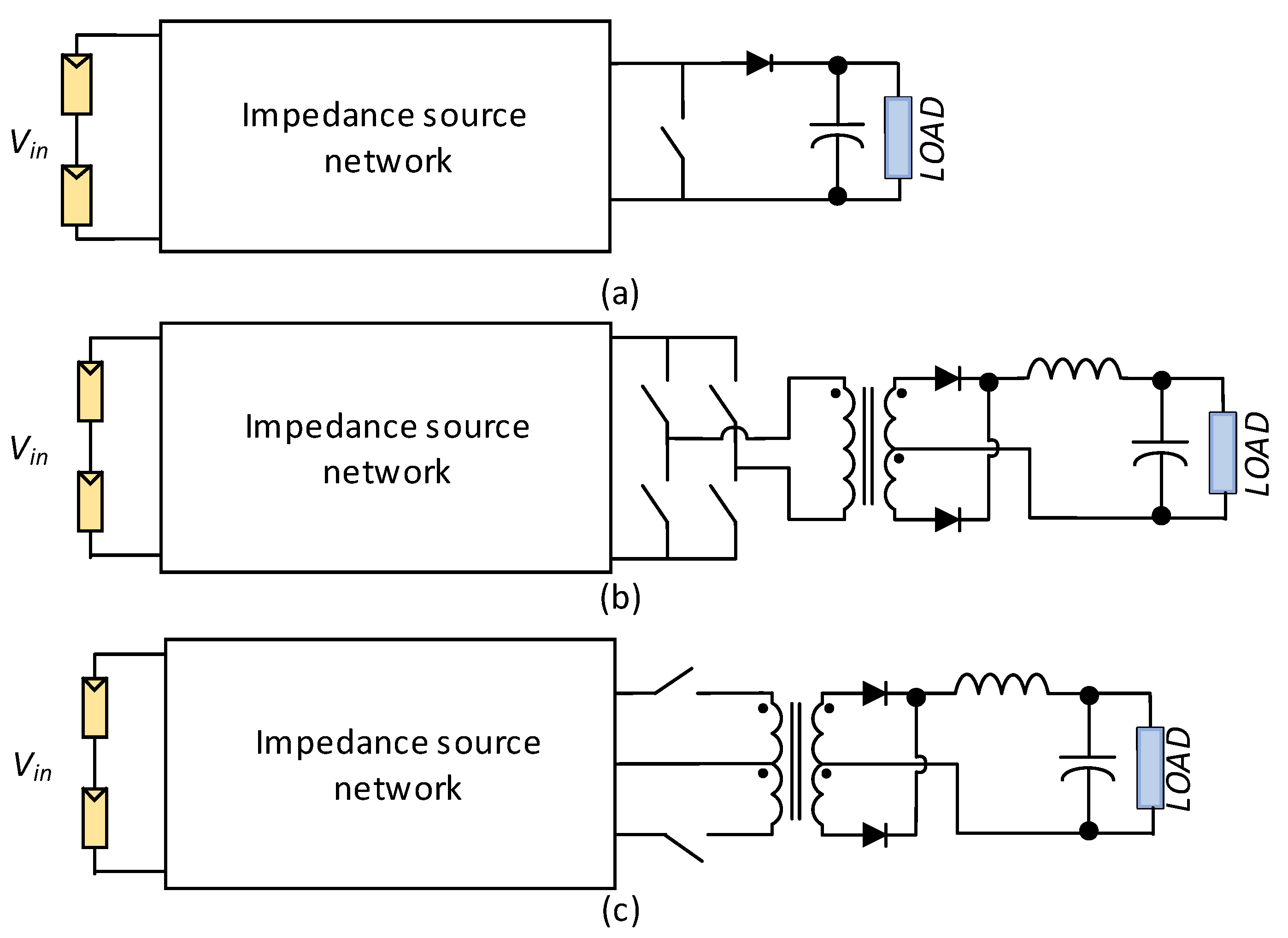
A front-end switching system in impedance-source DC/DC conversion systems includes a conventional single switch, a full-bridge, and a push-pull structure, as shown in Figure 2 [19]. Using full-bridge and push-pull switching systems provides input to output voltage isolation, which is preferred for some applications. As described below, voltage isolation proves the ability to apply the partial power processing technique, which results in performance improvement.
Several structures of impedance networks are presented, such as Z-source, T-source, Y-source, and A-source [20,21,22]. Compared to a traditional structure (Z-source), T-source requires a lower number of passive elements and coupling inductors, which provides higher voltage gain for the converter [22]. A total of two types of T-source converters, non-isolated and isolated, are depicted in Figure 3. In the isolated type, a voltage multiplier is connected to the output of the isolated winding of the transformer (Figure 3b).
The partial power processing technique is a technique which can be used to improve the voltage gain and efficiency of a converter. A DC/DC converter can be considered a DC transformer with a turns ratio of M(D), which is the converter voltage gain. Similar to the winding connection of an AC autotransformer, an isolated DC/DC converter can be changed to a PPC. In a PPC, a part of the energy is directly transferred to the output and only a fraction of power is processed by the converter; therefore, the converter performance can be improved. There are two main types of PPC structures [23]: input parallel output series (Figure 4a) and input series, output parallel (Figure 4b).
Using the partial power processing technique for non-isolated converters was investigated [23,24,25,26,27,28]. In this paper, this technique is applied to an isolated T-source DC/DC converter to improve the converter voltage gain. A total of two structures of this converter are proposed and compared for possible applications, including UPS systems. In Section 2, the proposed structures are presented and the main relations for steady-state operation of the converter are derived. In Section 3, conventional PPC and improved PPC and full-power converter (FPC) are compared. The simulation and experimental results of the presented converter are provided in Section 4.
2. Operation Principles
A total of two configurations of partial power for a T-source converter are presented here: conventional partial power T-source converter (PPTSC) and improved PPTSC. The schematics of the converters are shown in Figure 5a,b, respectively. As shown in Figure 5, in the conventional form, the series connection of input voltage and the voltage on the C3 capacitor creates the output voltage. In the improved form, C3 and C1 are in series in the output. As the C1 voltage is greater than the input voltage, higher voltage gain and improved performance are expected.
The converter circuit and current paths for two switching states are shown in Figure 6. During the ON state operation (Figure 6a), the voltage across the second winding (W2) (with a turns ratio of N2) is equal to C1 voltage (VC1) and the current goes through it; therefore, the current induces in the first and third windings (W1 and W3, respectively). This causes D1 and D2 to be turned off and D3 to be turned on. Magnetizing the current (Ilm), which is modelled in parallel with W1, decreases during this state. The W1 current (IW1) is equal to Ilm. The converter relationships during this switching state are as follows:
where IW2 and IW3 are the currents of W2 and W3 windings, respectively; Io is the output current of the converter in Figure 6; N3 is the turns ratio of W3; and VL is the voltage across magnetizing inductance. During the OFF state operation (Figure 6b), Ilm increases and D1 and D2 are ON while D3 is OFF. The converter relationships during this switching state are as follows:
Employing (1)–(9) and using the inductor volt second balance and capacitor charge balance rules, the steady-state relations are derived.
where D is the duty cycle of the switch.
The capacitor voltage and IlM ripples (∆VCi and ∆IlM) are calculated as:
All the relations for the steady-state analysis of the converters are derived, which can also be used for other analyses such as calculating the voltage and current stress on the elements and comparing the performance of the converters. In the next section, full-power TSC, conventional PPTSC, and improved PPTSC are compared in different terms.
3. Comparison of Full-Power TSC, Conventional PPTSC, and Improved PPTSC
To analyze the performance of the presented converters; full power TSC (FPTSC) (Figure 3b), conventional PPTSC (Figure 5a), and improved PPTSC (Figure 5b) are compared in terms of voltage gain, voltage and current stress on semiconductor devices, and converter efficiency. The fraction of power process (FPP) is shown in Figure 7. FPP is the proportion of total output power to the power processed by the converter and is one of the important values for comparison of PPCs [29]. Lower FPP is desirable as it is associated with less voltage and current stress on the elements and improves the converter performance. Figure 7 demonstrates that FPP is lower for the improved PPTSC.
In Figure 8, output voltage gain versus D is plotted and compared for three discussed converters in non-ideal conditions. The input voltage is 30 V. The value of non-idealities and converter parameters considered here are the same as the values mentioned for the prototype in Section 4. As shown in Figure 8, improved PPTSC shows a greater voltage gain for D < 0.3. Although the maximum achievable gain is achieved for the conventional PPTSC, the improved PPSC shows higher voltage gain for a wide range of duty cycle. In high values of D, the voltage drop of W1 is increased for improved PPTSC as a higher current passes through it. This limits the voltage gain of the improved PPTSC at high values of D.
The relationships for voltage and current stresses of the switches and diodes are shown in Table 1. The equations for voltage stress of any elements in all three converters are the same, but in similar operation conditions, i.e., the same input and output voltage, the required D for the improved PPTSC is lower and (1 − D)N2 − D (denominator of the voltage stress equation) is a decreasing function. Therefore, the voltage stress of the switch and diodes in the improved PPTSC is lower than the other two converters. Comparing the relations for current stress in Table 1 demonstrates that:
- The relations for the current stresses of the switch for all structures are the same. Although the relations are the same, lower D leads to lower current stress in PPTSC structures.
- The current stress of D2 and D3 are lower for improved PPTSC. The reason is the same as the above description. Although the relations are the same, a lower D leads to lower current stress in PPTSC structures.
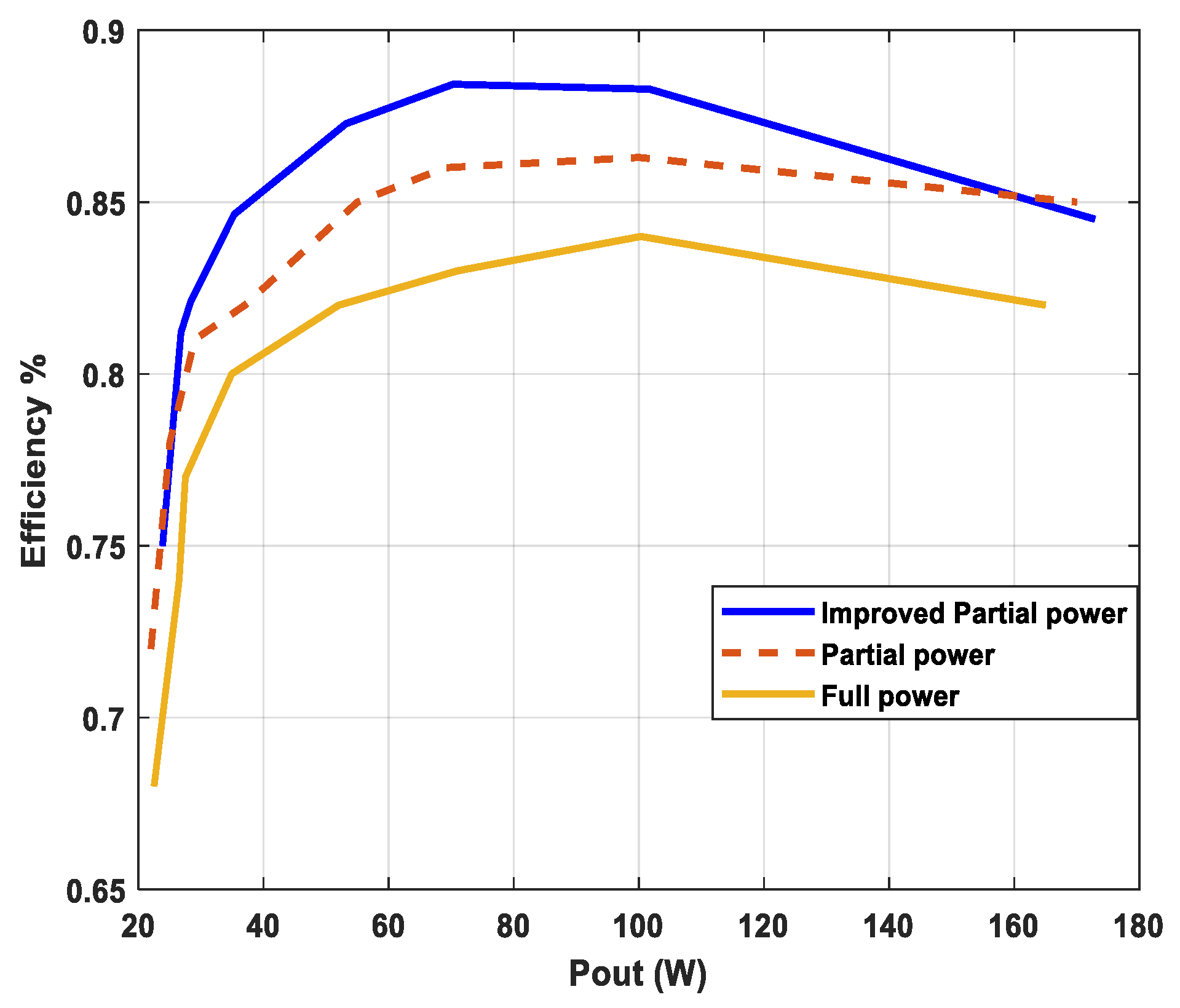
The efficiency comparison of the converters shown in Figure 9 was obtained according to the relations described [30] for conduction and switching losses of the converters.
The main non-idealities considered for the converters are metal oxide semiconductor field effect transistor (MOSFET) conduction resistance (Ron), transformer winding resistances (RW1, RW2, and RW3), and forward voltage of the diodes (Vf). Regarding these parasitic elements, the main power losses are as follows:
- Conduction losses of switches, transformer windings, and diodes.
- Turn-ON and turn-OFF switching losses of the switches.
The conduction loss of windings (PCOND(W)) can be calculated:
The expressions for the winding currents are extracted in Section 2 of the paper.
Using the root-mean-square (RMS) value of switch current and diode average current, the conduction losses of the switch and diodes (PCOND(S) and PCOND(D)) are given by (25) and (26), respectively.
MOSFET switching loss PSW is estimated based on the amount of dissipated energy ESW in the switches during turn-ON and turn-OFF transitions [31], and given by (27).
where,
The above equations are the same for all structures. The difference in the value of D for a given output (PP converters require a lower duty cycle) results in efficiency improvement using the PP structure.
The converter parameters used to plot the efficiency diagram are the same as the parameters used for simulation, which is discussed in the next section. Figure 9 demonstrates a higher efficiency of PPCs compared to the full power converter. Comparison of efficiency diagrams for improved and conventional PPTSCs shows that, for lower loads, improved PPTSC efficiency is better, while at high loads, conventional PPTSC improves. The main reason for this is related to the conduction loss of W1 winding and D1. Whereas W1 and D1 process full power in improved PPTSC, their currents are higher than conventional PPTSC; therefore, efficiency is limited in this case while the current that goes through them increases (higher loads). The region in which improved PPTSC has higher efficiency is related to the converter parameters, while winding resistance of W1 and forward voltage of D1 play an important role in this.
The same parasitic elements are considered for calculating the non-ideal voltage conversion ratio (VCR). Modifying the relationships in two switching states can provide the relationship. As the voltage drop on windings and switches depends on the winding and switch currents, respectively, it is almost impossible to derive a unique relation for VCR in non-ideal conditions. For obtained non-ideal VCR, Equations (2) and (6) can be modified as follows:
The current of W1 is the same for all structures; therefore, the current of other windings and the switch (which is equal to IW2) are lower for the improved PPTSC, which result in a lower voltage drop. The lower voltage drop on elements improves the non-ideal VCR of the improved PPTSC compared to the other structures.
4. Simulation and Experimental Result
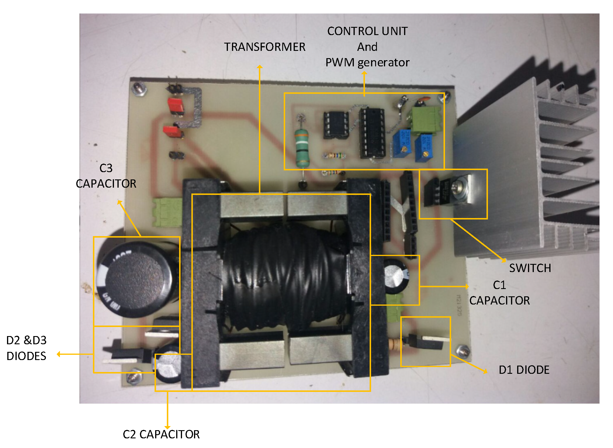
To verify the performance of the presented converters, several simulations were performed and a prototype converter was built (Figure 10). Several experimental tests are carried out and compared with simulations and theoretical analysis. The parameters are listed in Table 2.
A total of two structures (conventional PPTSC and improved PPTSC) with the same duty cycles (Figure 11a) were simulated and the results are shown in Figure 11. Drain-source voltage, voltage across the transformer windings, magnetizing current, and capacitor voltage are shown in Figure 11b–i, respectively, for two converters. As expected by theoretical analysis, during the first subinterval (the switch is turned on) magnetizing inductance, C3 charged while C1 and C2 discharged. Figure 11f shows that the peak value of magnetizing currents for both converters were maintained around constant values; therefore, an appropriate design of the transformer can guarantee it will work in the linear core region and prevent saturation. A disadvantage of the improved PPTSC compared to conventional PPTSC is related to the magnetizing current of the transformer. Figure 11f shows that the transformer magnetizing current for the improved PPTSC is higher than that of the conventional PPTSC. This is mainly because the first winding processes all the power and this part of the converter needs to be considered full power. This increases the peak value of the magnetizing current and affects the transformer design. The voltages of capacitors are regulated with a ripple of less than 0.1 V (0.5%). The ripple of the output voltage for both converters is less than 0.06%, and the proposed improved PPTSC has a higher voltage gain than the conventional PPTSC according to Figure 11j. Using the steady-state relations derived in the previous section and the simulation parameters listed in Table 2, the steady-state values for the capacitor voltages and magnetizing inductor currents were calculated as VC1 = 53 V, VC2 = 22 V, and VC3 = 105 V for both structures and IlM = 2.05 A and IlM = 3.25 A for conventional and improved PPTSC, respectively. The capacitor voltage is the same if similar duty cycles are applied to both structures. The obtained simulation results match the theoretical outcomes.
The experimental results of both presented converters are shown in Figure 12 and Figure 13. The experiments were performed similarly to simulations for better comparison. The obtained results match the theoretical analysis and simulation results. Figure 14 shows the converter efficiency for three structures based on experiments and simulations for different output powers. The difference between input and output power is considered the converter loss. This efficiency curve verifies the theoretical analysis that improved PPTSC has higher efficiency compared to a conventional PPTSC and a full-power converter.
5. Conclusions
In this paper, a new DC/DC converter was proposed for renewable energy integration in UPS systems by adapting a T-source converter in a partial power processing structure. This converter, compared to other impedance source converters, requires fewer components, and we showed that its efficiency is higher. The operation principle of this converter was presented, and governing relations were obtained. The presented comparisons proved that it has higher voltage gain, lower voltage, and current stresses on the semiconductors. Finally, the simulation and experimental results were presented to verify the performance of the converter.
Author Contributions
A.R. is the main researcher who initiated and organized research reported in the paper. He contributed to the sections on converter design, modeling, controlling, and writing the main parts of the paper. A.N. developed the prototype and performed the converter validation. M.S. (Mahdi Shahparasti) and M.S. (Mehdi Savaghebi) contributed to analysis, writing, and editing of the manuscript. All authors have read and agreed to the published version of the manuscript.
Funding
This research received no external funding.
Conflicts of Interest
The authors declare no conflict of interest.
References
- Shahparasti, M.; Yazdian, A.; Mohamadian, M.; Larijani, A.S.S.; Fatemi, A. Parallel uninterruptible power supplies based on Z-source inverters. IET Power Electron. 2012, 5, 1359. [Google Scholar] [CrossRef]
- Lu, J.; Guerrero, J.M.; Savaghebi, M.; Ghias, A.M.Y.M.; Guan, Y.; Hou, X.; Vasquez, J.C. An Effective Solution for Regeneration Protection in Uninterruptible Power Supply. IEEE Trans. Ind. Appl. 2019, 55, 3055–3065. [Google Scholar] [CrossRef]
- Zhang, W.; Xu, D.; Li, X.; Xie, R.; Li, H.; Dong, D.; Sun, C.; Chen, M. Seamless transfer control strategy for fuel cell uninterruptible power supply system. IEEE Trans. Power Electron. 2013, 28, 717–729. [Google Scholar] [CrossRef]
- Lu, J.; Savaghebi, M.; Golestan, S.; Vasquez, J.C.; Guerrero, J.M.; Marzabal, A. Multimode Operation for On-Line Uninterruptible Power Supply System. IEEE J. Emerg. Sel. Top. Power Electron. 2019, 7, 1181–1196. [Google Scholar] [CrossRef] [Green Version]
- Li, W.; He, X. Review of nonisolated high-step-up DC/DC converters in photovoltaic grid-connected applications. IEEE Trans. Ind. Electron. 2011, 58, 1239–1250. [Google Scholar] [CrossRef]
- Silva, R.V.; Freitas, A.A.A.; Castro, M.R.; Antunes, F.L.M.; Sa, E.M. High gain QZS DC/DC converter with coupled inductor and capacitor switch. In Proceedings of the 2015 IEEE 13th Brazilian Power Electronics Conference and 1st Southern Power Electronics Conference (COBEP/SPEC), Fortaleza, Brazil, 29 November–2 December 2015; pp. 1–6. [Google Scholar]
- Xuewei, P.; Rathore, A.K. Novel Soft-Switching Snubberless Naturally Front-End-Converter-Based Bidirectional Inverter for. IEEE Trans. Ind. Appl. 2014, 50, 4132–4141. [Google Scholar] [CrossRef]
- Forouzesh, M.; Siwakoti, Y.P.; Gorji, S.A.; Blaabjerg, F.; Lehman, B. Step-Up DC-DC converters: A comprehensive review of voltage-boosting techniques, topologies, and applications. IEEE Trans. Power Electron. 2017, 32, 9143–9178. [Google Scholar] [CrossRef]
- Adamowicz, M. Non-isolated resonant quasi-Z-source network DC–DC converter. Electron. Lett. 2019, 55, 855–857. [Google Scholar] [CrossRef]
- Bajestan, M.M.; Shahparasti, M.; Khaburi, D.A. Application of trans Z-source inverter in photovoltaic systems. In Proceedings of the 2013 21st Iranian Conference on Electrical Engineering (ICEE), Mashhad, Iran, 14–16 May 2013; pp. 1–6. [Google Scholar]
- Shahparasti, M.; Rajaei, A.H.; Yazdian, A.; Mohamadian, M. Interline unified power quality conditioner based on single stage nine switch inverter. In Proceedings of the 2012 3rd Power Electronics and Drive Systems Technology (PEDSTC), Tehran, Iran, 15–16 February 2012; pp. 319–323. [Google Scholar]
- Shahparasti, M. Distributed Generation Inverter: New control Strategies to Supply Local Load with Standard Voltage under Distorted Grid Voltage. J. Energy Manag. Technol. 2019, 3, 1–10. [Google Scholar] [CrossRef]
- Lopez-Santos, O.; Garcia, G.; Martinez-Salamero, L.; Giral, R.; Vidal-Idiarte, E.; Merchan-Riveros, M.C.; Moreno-Guzman, Y. Analysis, design, and implementation of a static conductance-based MPPT method. IEEE Trans. Power Electron. 2019, 34, 1960–1979. [Google Scholar] [CrossRef]
- Shahparasti, M.; Sadeghi Larijani, A.; Fatemi, A.; Yazdian Varjani, A.; Mohammadian, M. Quasi Z-source inverter for photovoltaic system connected to single phase AC grid. In Proceedings of the 2010 1st Power Electronic & Drive Systems & Technologies Conference (PEDSTC), Tehran, Iran, 17–18 February 2010; pp. 456–460. [Google Scholar]
- Siwakoti, Y.P.; Blaabjerg, F.; Loh, P.C. Quasi-Y-source inverter. In Proceedings of the 2015 Australasian Universities Power Engineering Conference (AUPEC), Wollongong, Australia, 27–30 September 2015; Volume 1, pp. 1–5. [Google Scholar]
- Sajadian, S.; Ahmadi, R.; Zargarzadeh, H. Extremum Seeking-Based Model Predictive MPPT for Grid-Tied Z-Source Inverter for Photovoltaic Systems. IEEE J. Emerg. Sel. Top. Power Electron. 2019, 7, 216–227. [Google Scholar] [CrossRef]
- Siwakoti, Y.P.; Peng, F.Z.; Blaabjerg, F.; Loh, P.C.; Town, G.E.; Yang, S. Impedance-source networks for electric power conversion part II: Review of control and modulation techniques. IEEE Trans. Power Electron. 2015, 30, 1887–1906. [Google Scholar] [CrossRef]
- Siwakoti, Y.P.; Peng, F.Z.; Blaabjerg, F.; Loh, P.C.; Town, G.E. Impedance-source networks for electric power conversion Part I: A topological review. IEEE Trans. Power Electron. 2015, 30, 699–716. [Google Scholar] [CrossRef]
- Hakemi, A.; Sanatkar-Chayjani, M.; Monfared, M. Δ-Source Impedance Network. IEEE Trans. Ind. Electron. 2017, 64, 7842–7851. [Google Scholar] [CrossRef]
- Kong, X.; Wong, C.K.; Lam, C.S. Effects of Parasitic Resistances on Magnetically Coupled Impedance-Source Networks. IEEE Trans. Power Electron. 2020, 35, 9171–9183. [Google Scholar] [CrossRef]
- Liu, H.; Ji, Y.; Wang, L.; Wheeler, P. A family of improved magnetically coupled impedance network boost DC-DC converters. IEEE Trans. Power Electron. 2018, 33, 3697–3702. [Google Scholar] [CrossRef]
- Liu, H.; Zhou, B.; Li, Y.; Chen, J.; Loh, P.C. High-Efficiency T-Source Inverter with Low Voltage Spikes across the Switch Bridge. IEEE Trans. Power Electron. 2020, 35, 10554–10566. [Google Scholar] [CrossRef]
- Zhao, J.; Yeates, K.; Han, Y. Analysis of high efficiency DC/DC converter processing partial input/output power. In Proceedings of the 2013 IEEE 14th Workshop on Control and Modeling for Power Electronics (COMPEL), Salt Lake City, UT, USA, 23–26 June 2013; pp. 1–8. [Google Scholar]
- Gao, W.; Zhang, Y.; Lv, X.Y.; Lou, Q.M. Non-isolated high-step-up soft switching DC/DC converter with low-voltage stress. IET Power Electron. 2017, 10, 120–128. [Google Scholar] [CrossRef]
- Kim, K.; Cha, H.; Kim, H.G. A new single-phase switched-coupled-inductor DC-AC inverter for photovoltaic systems. IEEE Trans. Power Electron. 2017, 32, 5016–5022. [Google Scholar] [CrossRef]
- Ahmad, M.W.; Anand, S. Power decoupling in solar PV system using partial power processing converter. In Proceedings of the 2016 10th International Conference on Compatibility, Power Electronics and Power Engineering (CPE-POWERENG), Bydgoszcz, Poland, 29 June–1 July 2016; pp. 196–201. [Google Scholar]
- Sathyan, S.; Suryawanshi, H.M.; Singh, B.; Chakraborty, C.; Verma, V.; Ballal, M.S. ZVS-ZCS High Voltage Gain Integrated Boost Converter for DC Microgrid. IEEE Trans. Ind. Electron. 2016, 63, 6898–6908. [Google Scholar] [CrossRef]
- Levron, Y.; Clement, D.R.; Choi, B.; Olalla, C.; Maksimovic, D. Control of submodule integrated converters in the isolated-port differential power-processing photovoltaic architecture. IEEE J. Emerg. Sel. Top. Power Electron. 2014, 2, 821–832. [Google Scholar] [CrossRef]
- Nabinejad, A.; Rajaei, A.; Mardaneh, M. A Systematic Approach to Extract State-Space Averaged Equations and Small-Signal Model of Partial-Power Converters. IEEE J. Emerg. Sel. Top. Power Electron. 2019, 8, 2475–2483. [Google Scholar] [CrossRef]
- Rajaei, A.; Khazan, R.; Mahmoudian, M.; Mardaneh, M.; Gitizadeh, M. A Dual Inductor High Step-Up DC/DC Converter Based on the Cockcroft-Walton Multiplier. IEEE Trans. Power Electron. 2018, 33, 9699–9709. [Google Scholar] [CrossRef]
- Schirone, L.; Macellari, M. Loss Analysis of Low-Voltage TLNPC Step-Up Converters. IEEE Trans. Ind. Electron. 2014, 61, 6081–6090. [Google Scholar] [CrossRef]
Figure 1.
Online uninterruptible power supply (UPS) with photovoltaic (PV) connection.

Figure 2.
Different configuration of the front-end switching system in DC/DC impedance source converter. (a) single switch switching system, (b) full-bridge switching system, and (c) push-pull switching system.
Figure 2.
Different configuration of the front-end switching system in DC/DC impedance source converter. (a) single switch switching system, (b) full-bridge switching system, and (c) push-pull switching system.

Figure 3.
Configuration of T-source impedance network. (a) non-isolated and (b) isolated structures.
Figure 3.
Configuration of T-source impedance network. (a) non-isolated and (b) isolated structures.
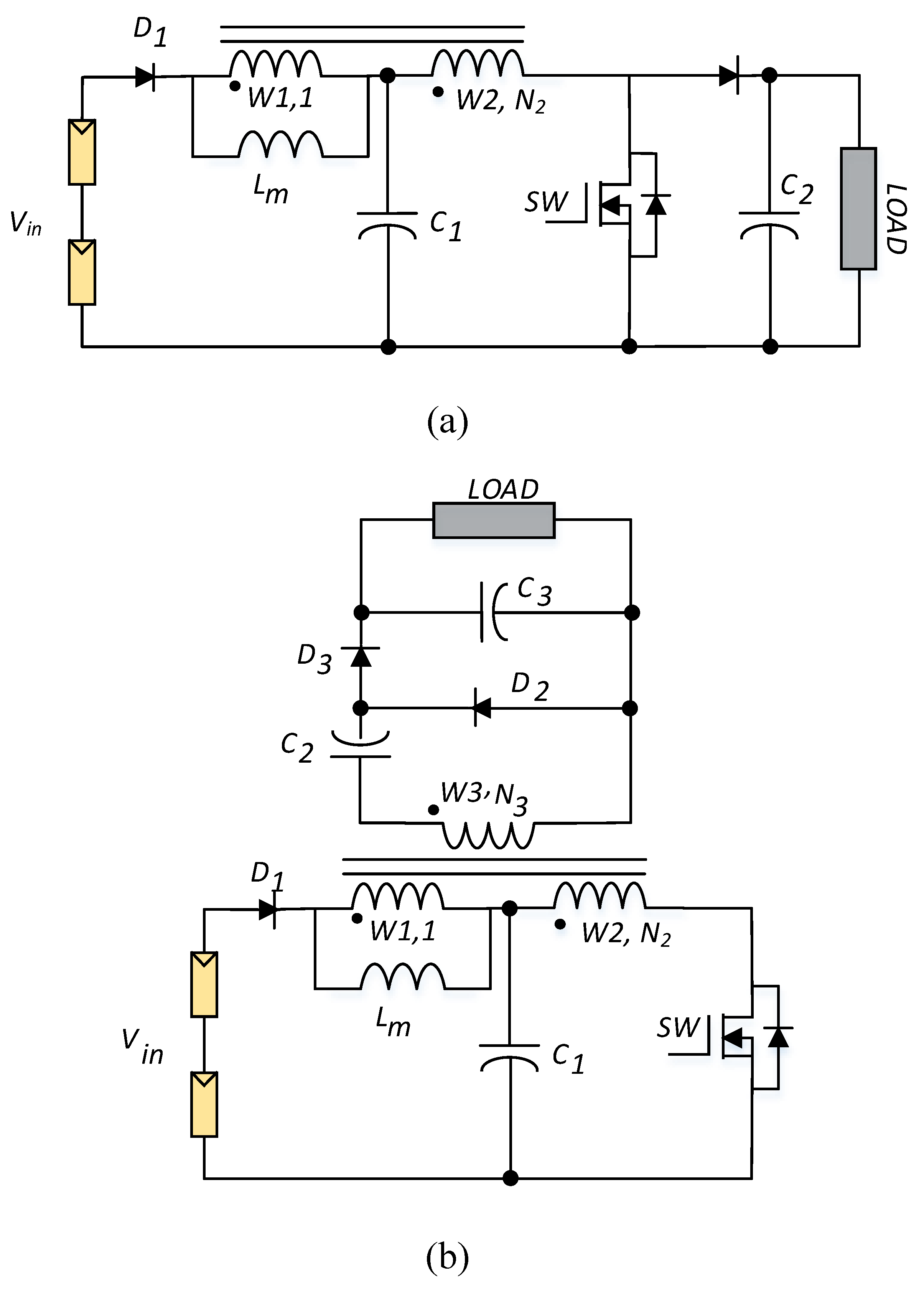
Figure 4.
Schematic diagram of PPC structures: (a) input parallel, output series, (b) input series, output parallel.
Figure 4.
Schematic diagram of PPC structures: (a) input parallel, output series, (b) input series, output parallel.
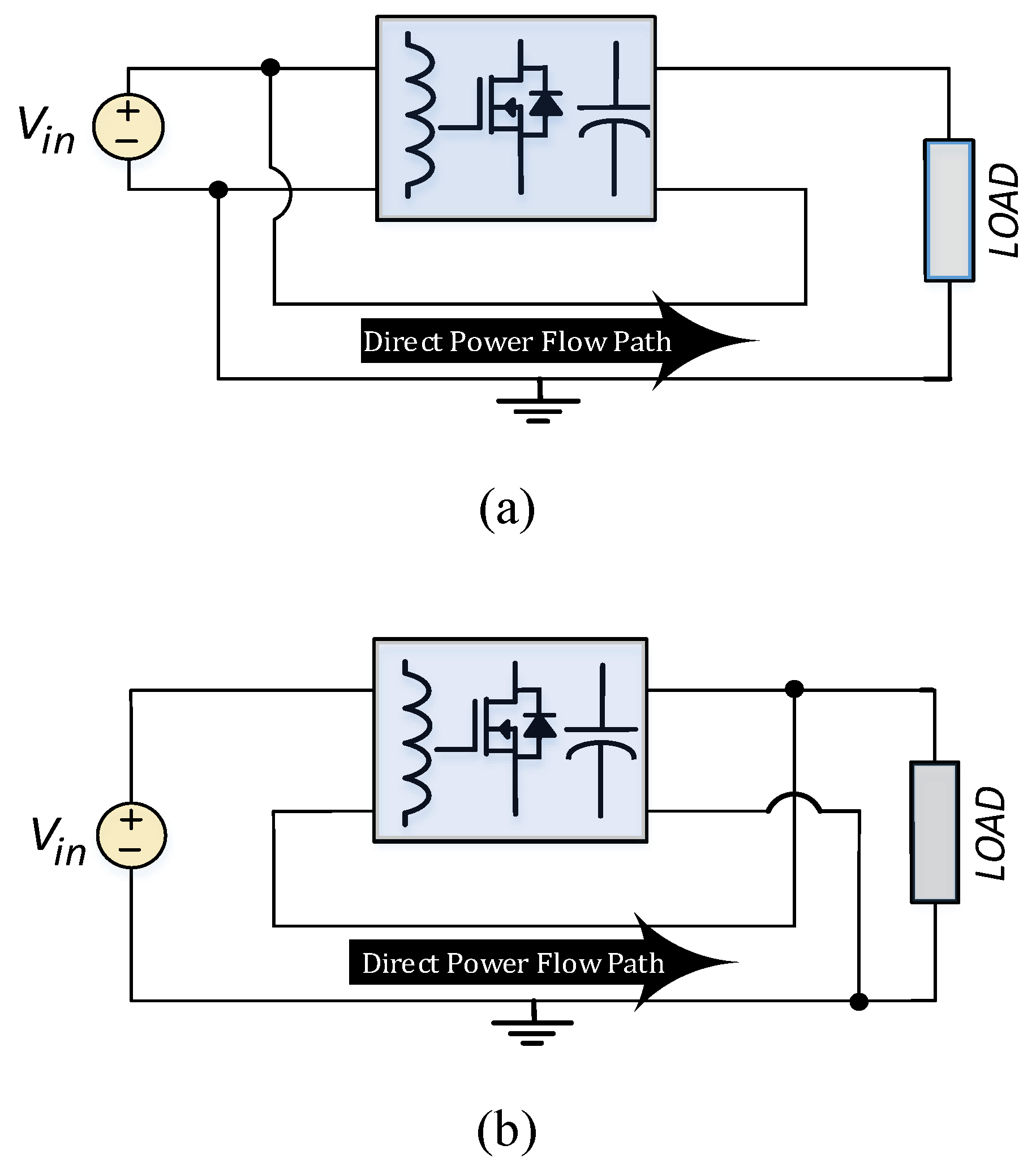
Figure 5.
Schematic of the proposed PPC: (a) conventional partial power processing T-source converter (PPTSC) and (b) improved PPTSC.
Figure 5.
Schematic of the proposed PPC: (a) conventional partial power processing T-source converter (PPTSC) and (b) improved PPTSC.
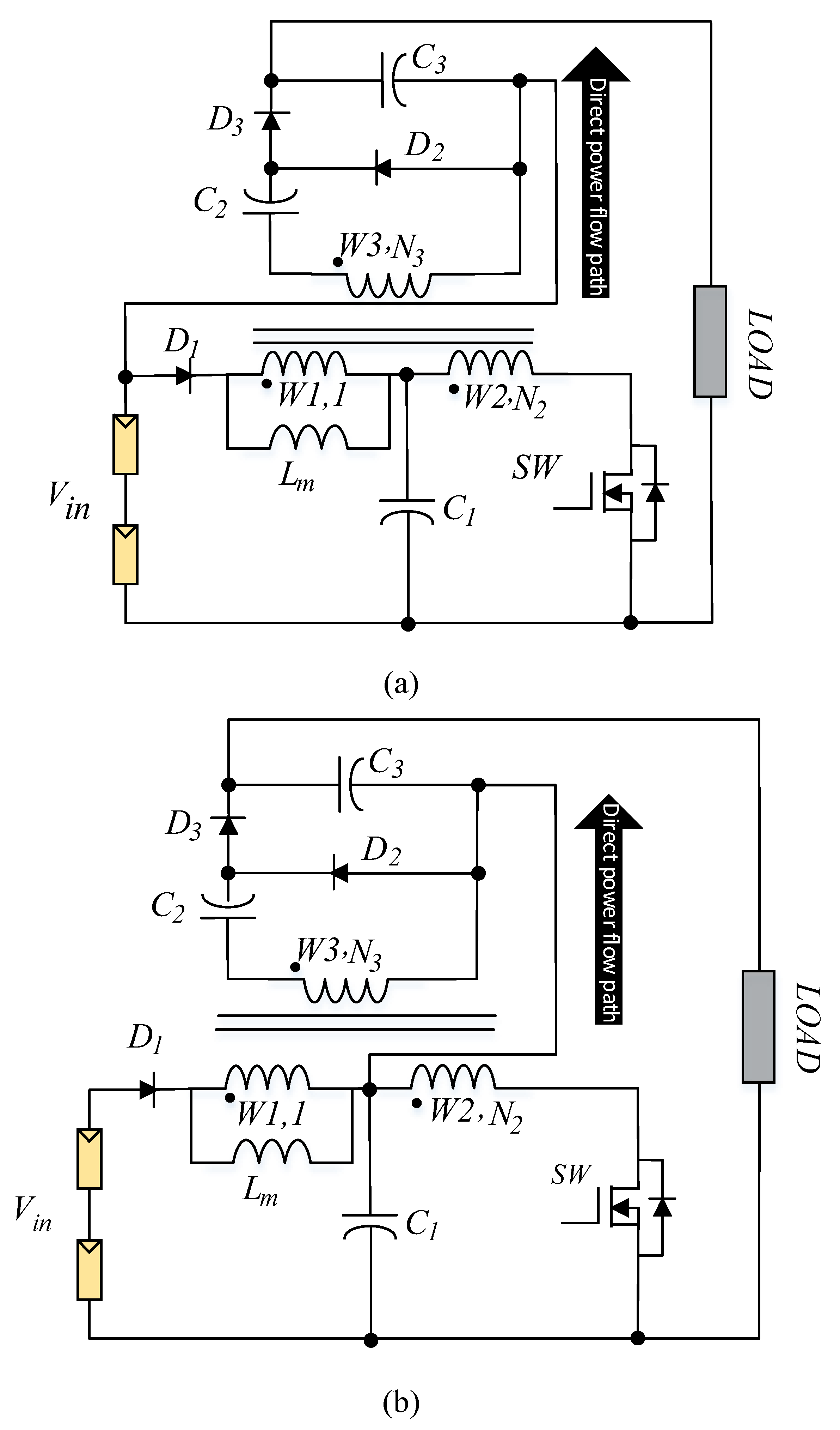
Figure 6.
Current paths in different switching states for improved PPTSC. (a) ON state operation and (b) OFF state operation.
Figure 6.
Current paths in different switching states for improved PPTSC. (a) ON state operation and (b) OFF state operation.
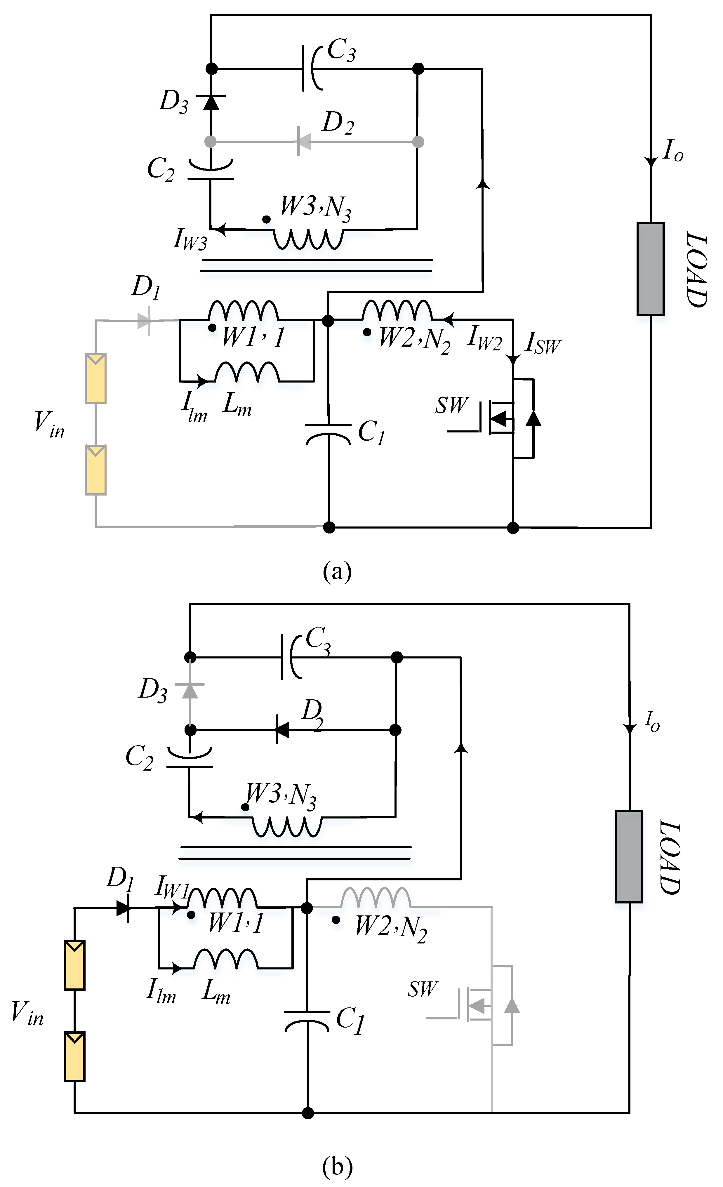
Figure 7.
Fraction of power process (FPP) comparison of conventional and improved PPTSC.

Figure 8.
Output voltage gain versus duty cycle for FPTSC, conventional PPTSC, and improved PPTSC.
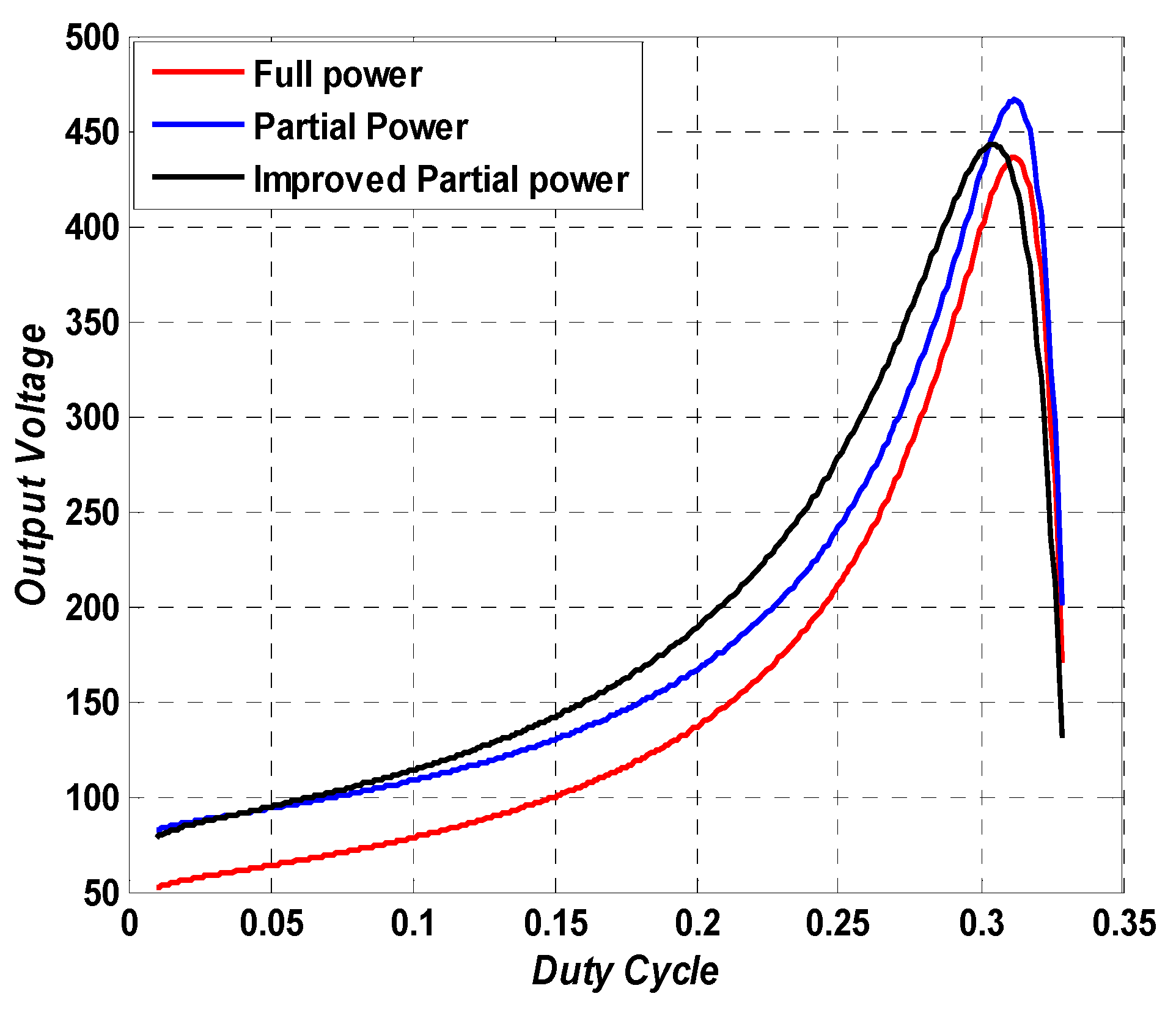
Figure 9.
Converter efficiency versus output power for conventional PPTSC, improved PPTSC, and FPTSC.
Figure 9.
Converter efficiency versus output power for conventional PPTSC, improved PPTSC, and FPTSC.
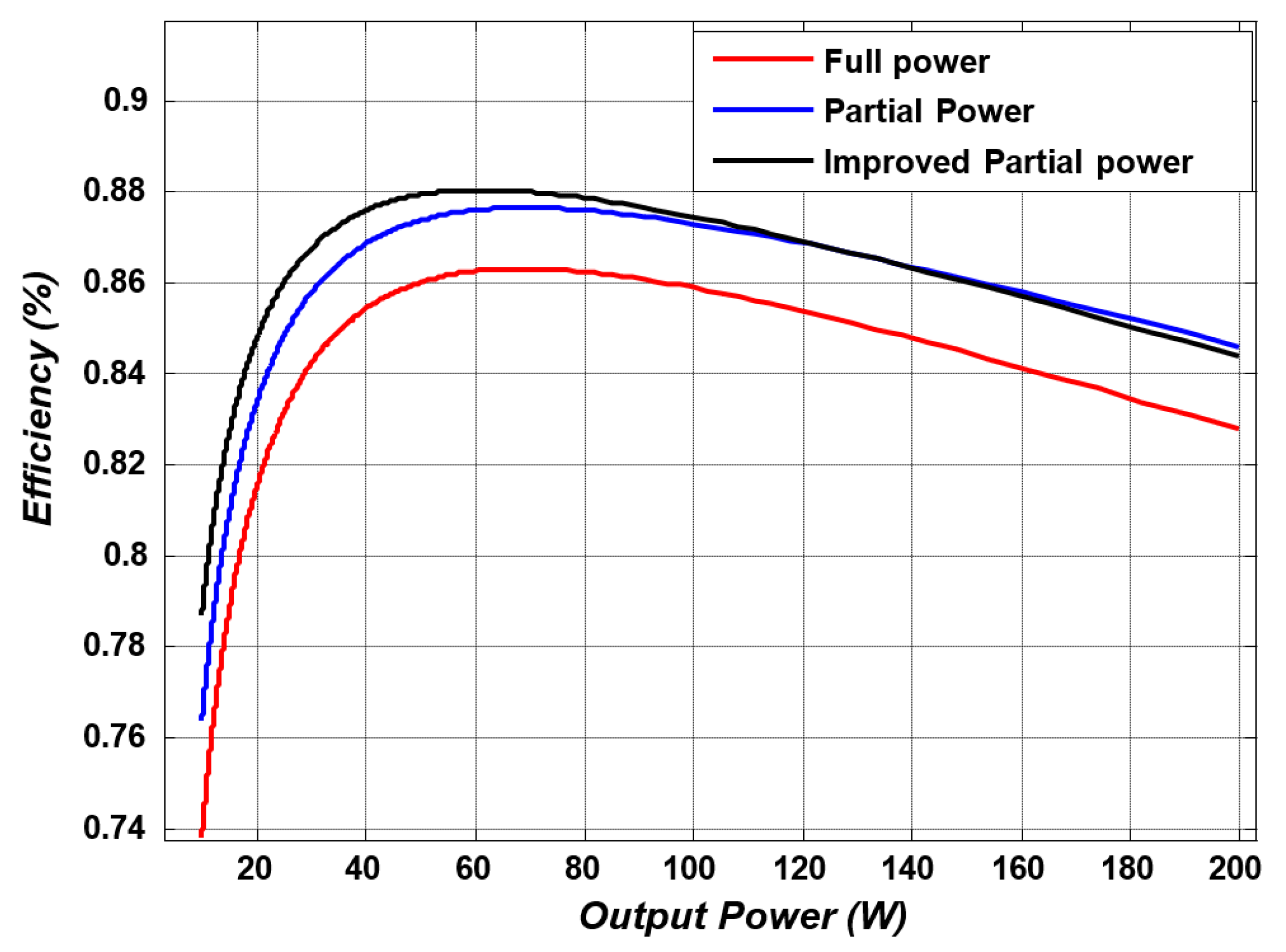
Figure 10.
Laboratory prototype.

Figure 11.
Simulation results for the proposed converters, left: conventional PPTSC, right: improved PPTSC. (a) Command signal, (b) switch drain-source voltage, (c) first winding voltage, (d) second winding voltage, (e) third winding voltage, (f) magnetizing current, (g)VC1, (h)VC2, (i)VC3, and (j) output voltage.
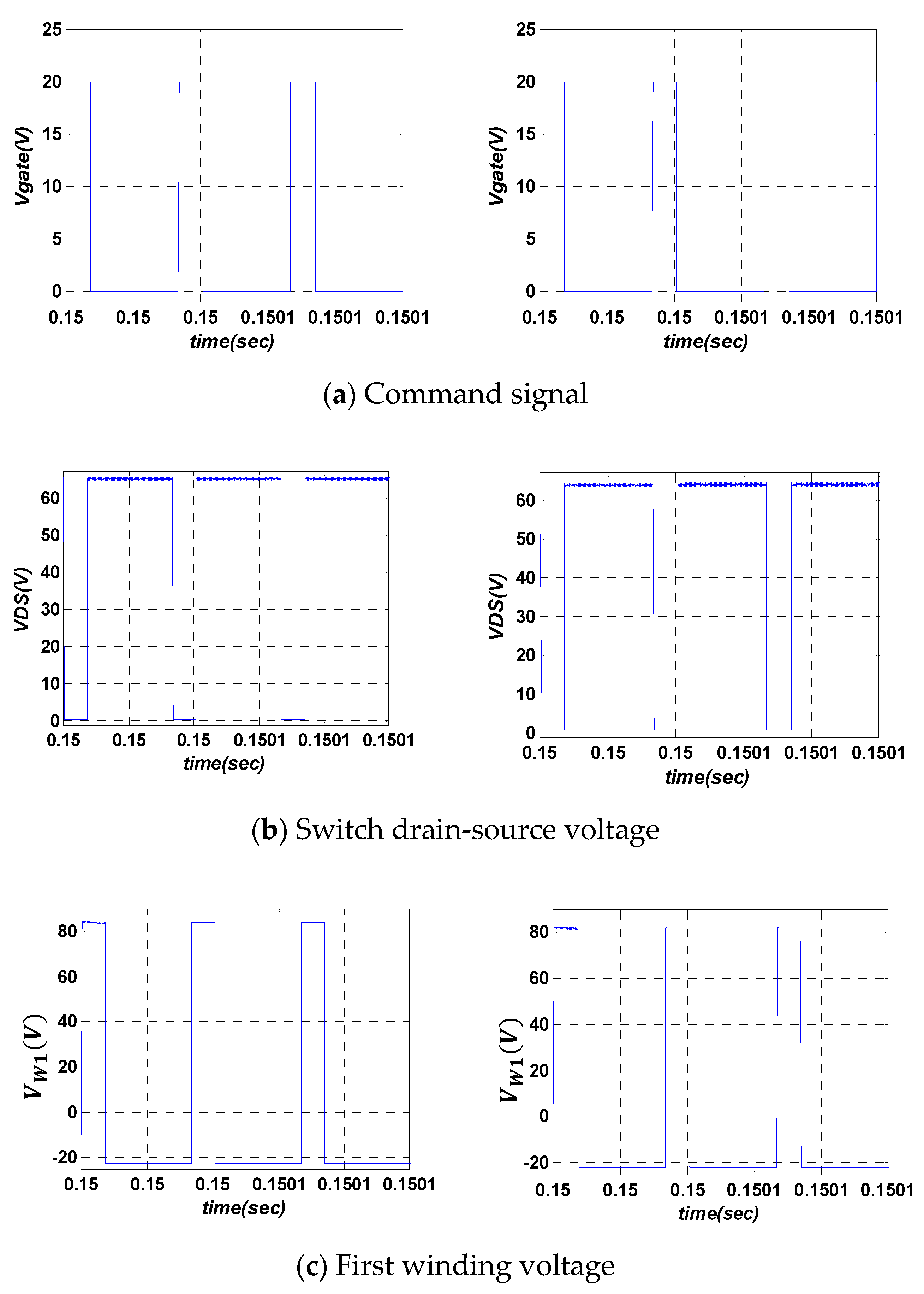
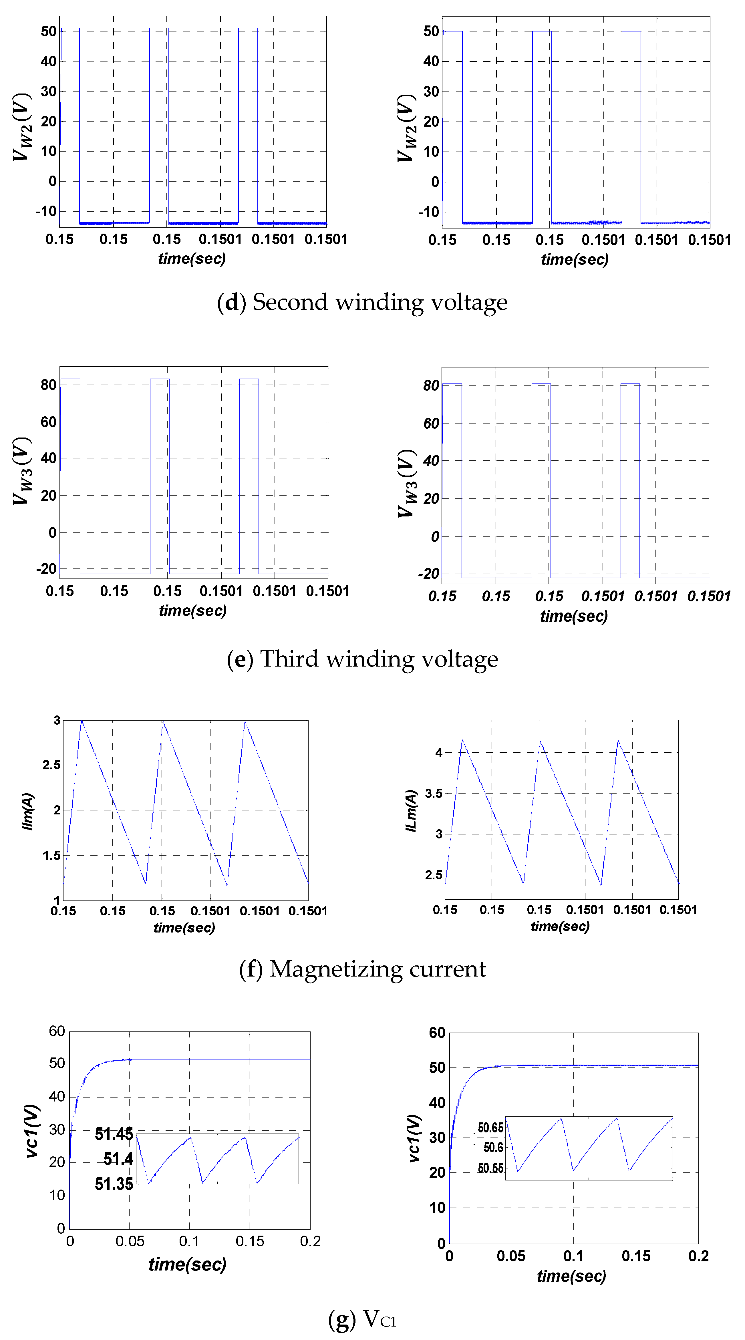

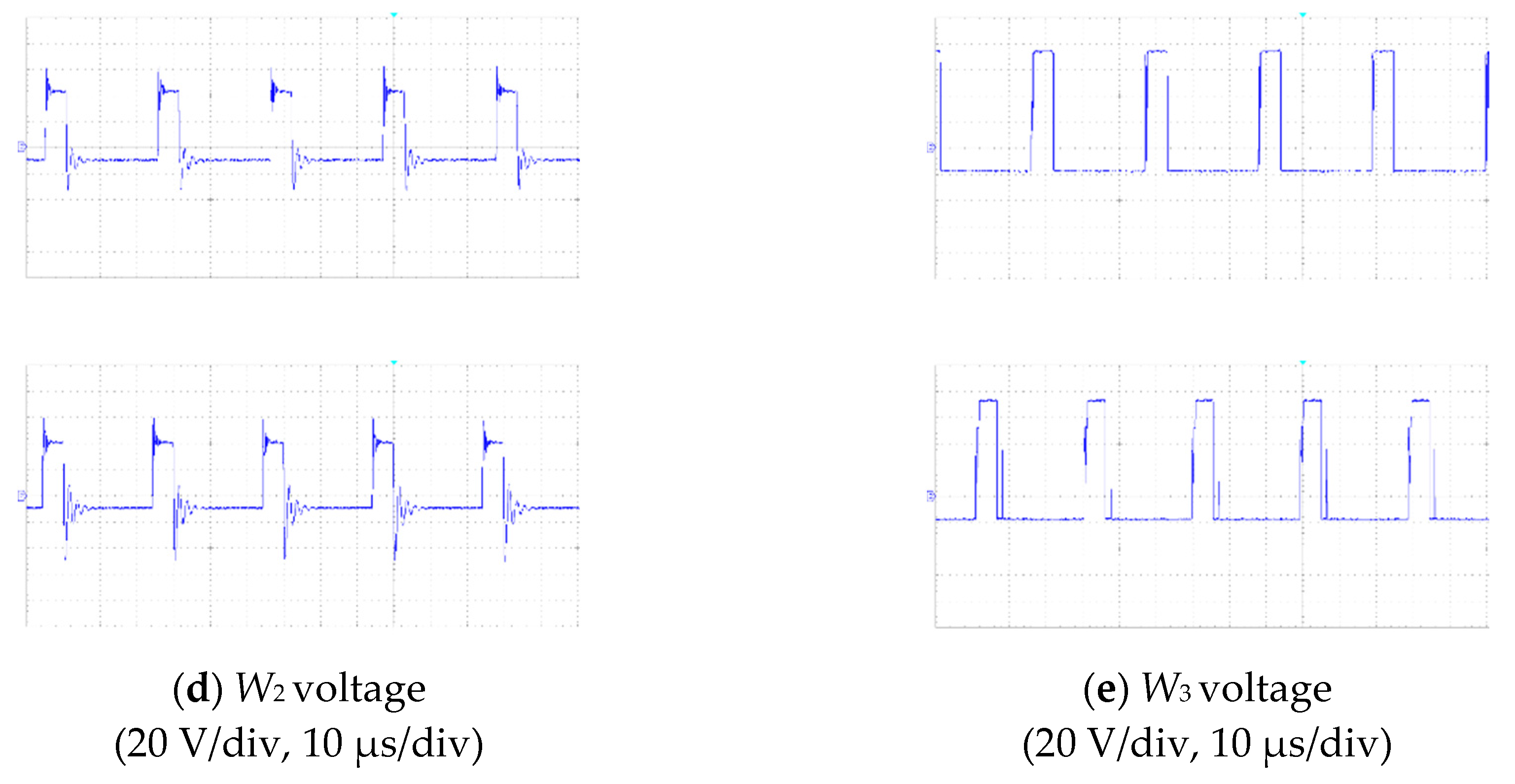
Figure 12.
Experimental results for the proposed converters, left: conventional PPTSC, right: improved PPTSC: (a) ate voltage, (b) switch drain-source voltage, (c) first winding voltage, (d) second winding voltage, and (e) third winding voltage.
Figure 12.
Experimental results for the proposed converters, left: conventional PPTSC, right: improved PPTSC: (a) ate voltage, (b) switch drain-source voltage, (c) first winding voltage, (d) second winding voltage, and (e) third winding voltage.
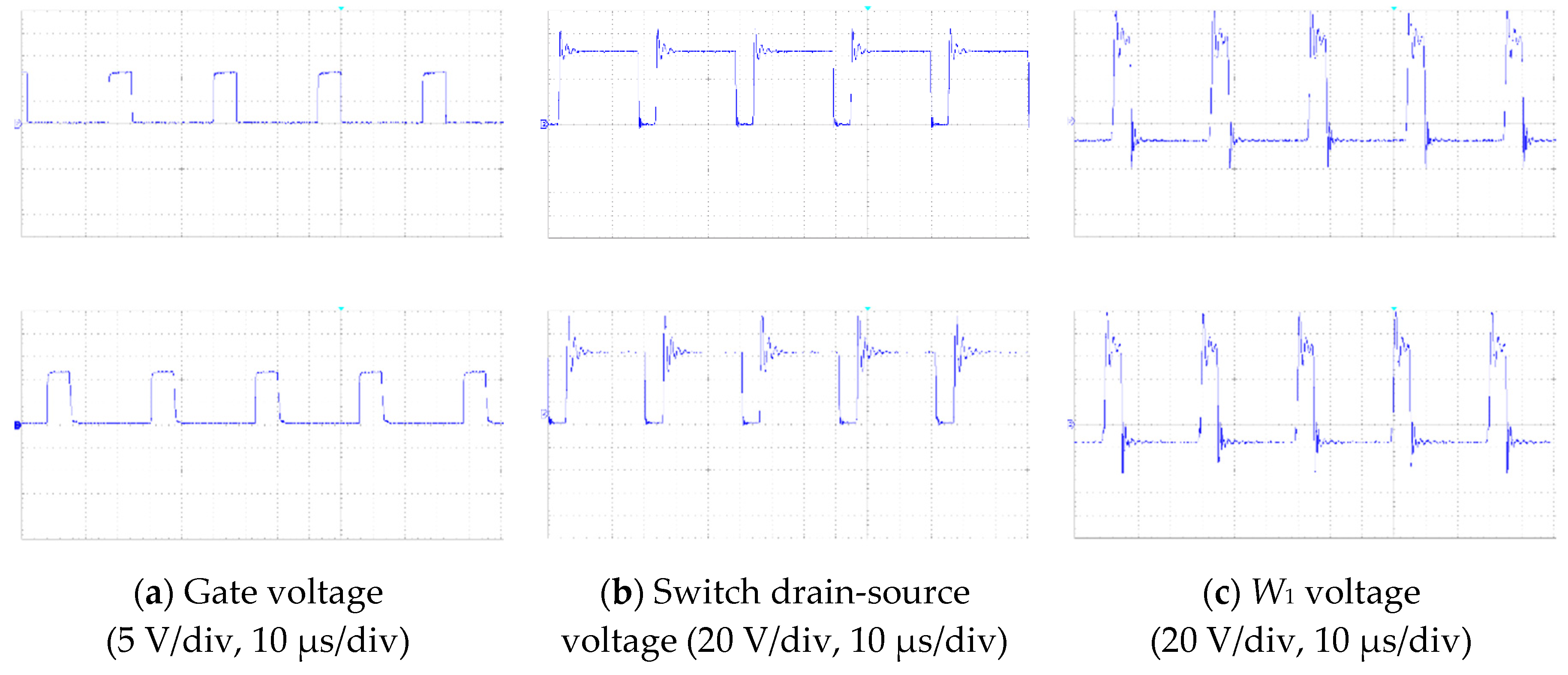

Figure 13.
Experimental results for the capacitor voltage and output voltage of the proposed converters, left: conventional PPTSC, right: improved PPTSC. (a) VC1, (b)VC2, (c)VC3, and (d) output and input voltage.
Figure 13.
Experimental results for the capacitor voltage and output voltage of the proposed converters, left: conventional PPTSC, right: improved PPTSC. (a) VC1, (b)VC2, (c)VC3, and (d) output and input voltage.
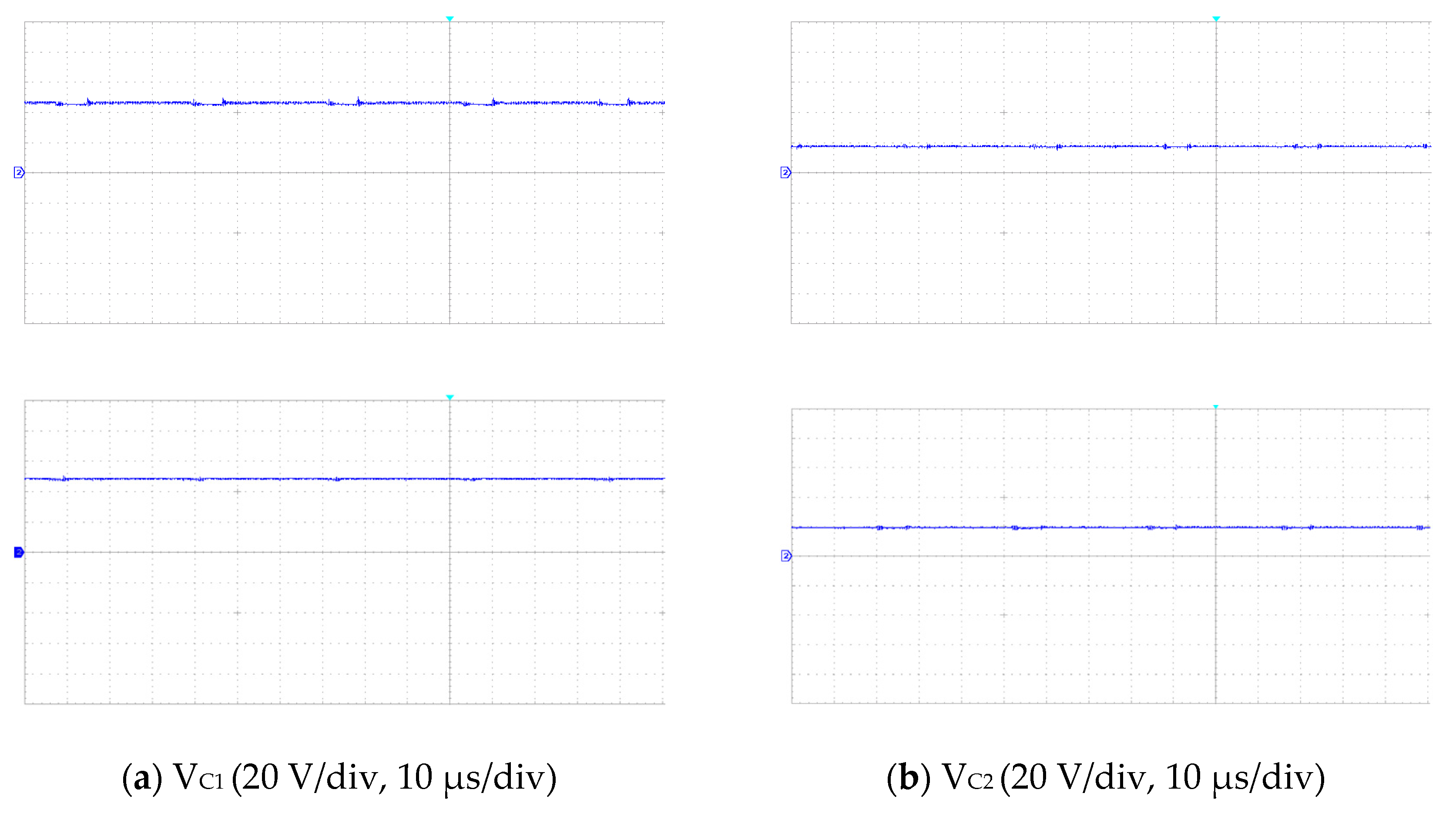
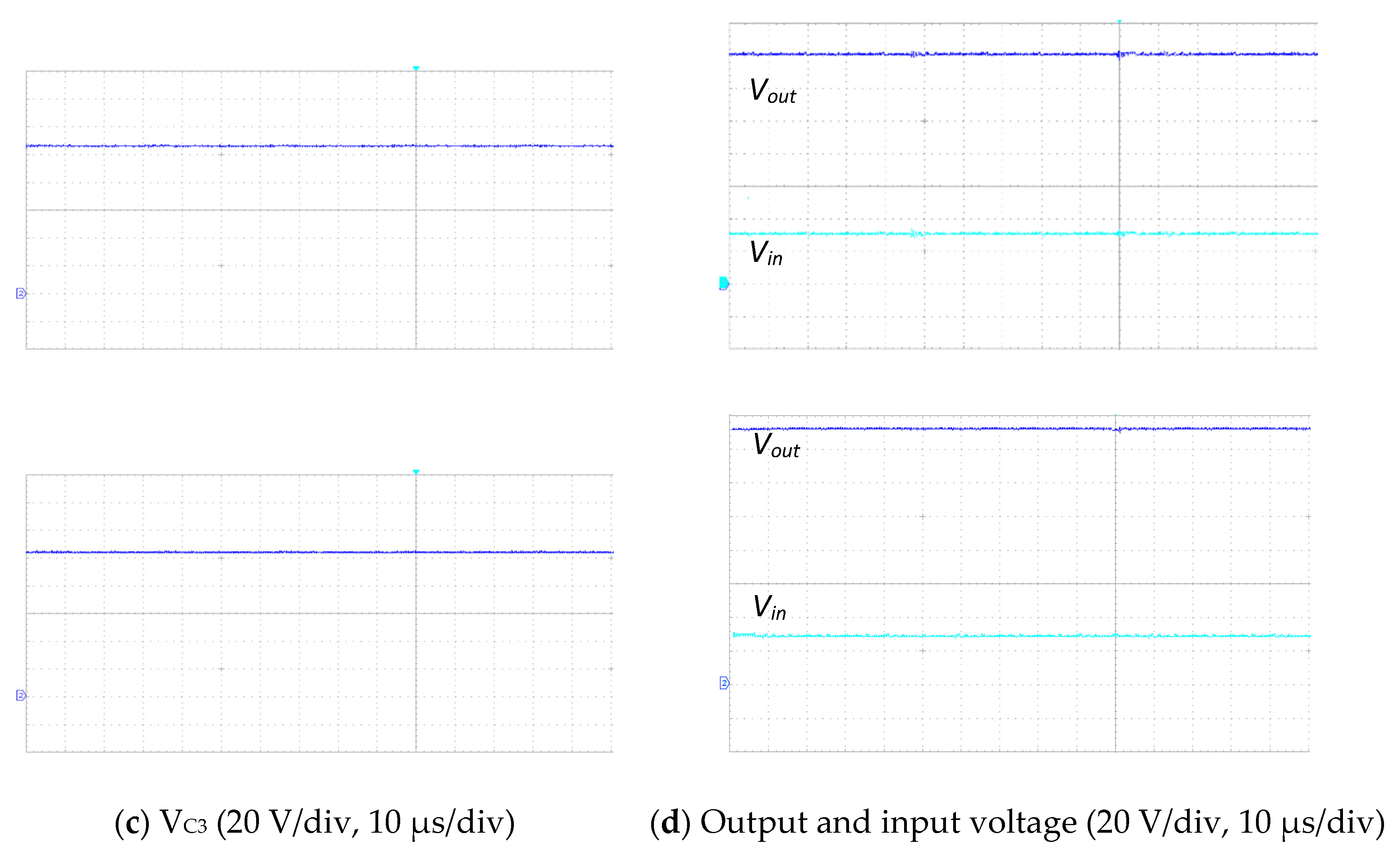
Figure 14.
Converter efficiency versus output power for conventional PPTSC, improved PPTSC, and FPTSC.
Figure 14.
Converter efficiency versus output power for conventional PPTSC, improved PPTSC, and FPTSC.

Table 1.
Voltage and current stress of the switches and diodes for FPTSC, conventional PPTSC, and improved PPTSC.
Table 1.
Voltage and current stress of the switches and diodes for FPTSC, conventional PPTSC, and improved PPTSC.
| FPTSC | Conventional PPTSC | Improved PPTSC | |
|---|---|---|---|
| Gain | |||
Table 2.
Simulation and experimental parameters.
| Parameter | Symbol | Value |
|---|---|---|
| Input voltage | Vin | 30 V |
| Output voltage | Vout | 150 V |
| Load | R | 400 Ω |
| Switching frequency | f | 30 kHz |
| Turns ratio of three winding transformer | 1:N2:N3 | 00:06.6 |
| Magnetizing inductance | Llm | 330 µH |
| Capacitance | C1, C2, C3 | 470 µF |
| Diode forward voltage | Vf | 1.2 V |
| Conduction resistance of switch | Ron | 0.09 Ω |
| First winding resistance | R1 | 0.2 Ω |
| Second winding resistance | R2 | 0.1 Ω |
| Third winding resistance | R3 | 0.3 Ω |
Publisher’s Note: MDPI stays neutral with regard to jurisdictional claims in published maps and institutional affiliations. |
© 2020 by the authors. Licensee MDPI, Basel, Switzerland. This article is an open access article distributed under the terms and conditions of the Creative Commons Attribution (CC BY) license (http://creativecommons.org/licenses/by/4.0/).
Share and Cite
MDPI and ACS Style
Rajaei, A.; Shahparasti, M.; Nabinejad, A.; Savaghebi, M. A High Step-Up Partial Power Processing DC/DC T-Source Converter for UPS Application. Sustainability 2020, 12, 10464. https://doi.org/10.3390/su122410464
AMA Style
Rajaei A, Shahparasti M, Nabinejad A, Savaghebi M. A High Step-Up Partial Power Processing DC/DC T-Source Converter for UPS Application. Sustainability. 2020; 12(24):10464. https://doi.org/10.3390/su122410464
Chicago/Turabian StyleRajaei, Amirhossein, Mahdi Shahparasti, Ali Nabinejad, and Mehdi Savaghebi. 2020. "A High Step-Up Partial Power Processing DC/DC T-Source Converter for UPS Application" Sustainability 12, no. 24: 10464. https://doi.org/10.3390/su122410464
Note that from the first issue of 2016, this journal uses article numbers instead of page numbers. See further details here.