

Stencil-Printed Scalable Radial Thermoelectric Device Using Sustainable Manufacturing Methods
by
 ,
,
Eunhwa Jang
1,
Rohan B. Ambade
2,3,
Priyanshu Banerjee
1,
L. D. Timmie Topoleski
1 and
Deepa Madan
1,* 1
Department of Mechanical Engineering, University of Maryland Baltimore County, 1000 Hilltop Circle, Baltimore, MD 21250, USA
2
Advanced Research & Innovation Center, Aerospace Engineering, Khalifa University of Science & Technology, Abu Dhabi 127788, United Arab Emirates
3
Department of Aerospace Engineering, Khalifa University of Science & Technology, Abu Dhabi 127788, United Arab Emirates
*
Author to whom correspondence should be addressed.
Sustainability 2024, 16(9), 3560; https://doi.org/10.3390/su16093560
Submission received: 13 February 2024
/
Revised: 29 March 2024
/
Accepted: 19 April 2024
/
Published: 24 April 2024
(This article belongs to the Special Issue Progress in Sustainable and Clean Energy Technologies)
Abstract
:In this study, we used n-chitosan-Bi2Te2.7Se0.3 and p-chitosan-Bi0.5Sb1.5Te3 composite inks to print a circular thermoelectric generator (TEG) device using a low-energy-input curing method. Thermoelectric (TE) composite films were fabricated using varying sizes of thermoelectric particles and a small chitosan binder (0.05 wt. %). The particles and binder were hot pressed at an applied pressure of 200 MPa and cured at 200 °C for 30 min. We achieved ZT of 0.35 for the n-type and 0.7 for the p-type TE composite films measured at room temperature. A radial TEG was fabricated using the best-performing n-type and p-type composite inks and achieved a power output of 87 µW and a power density of 727 µW/cm2 at a temperature difference of 35 K; these are among the best-reported values for printed TEG devices. Using a low-energy-input fabrication method, we eliminated the need for high-temperature and long-duration curing processes to fabricate printing devices. Thus, we envisage that the low-energy-input curing process and cost-effective printable strategy presented in this work pave the way for sustainable manufacturing of large-scale energy harvesting TEG devices.
1. Introduction
The recent advancements in wireless technology and the Internet of Things (IoT) have led researchers to develop wireless sensors for various applications. This includes wearable health monitoring devices, condition-monitoring wireless sensor network (WSN) devices used in defense applications, home appliances, industry, etc. [1,2]. WSN is a rapidly emerging technology used to monitor and collect physical data such as temperature, pressure, steam, structural health of bridges, etc. [3]. To continuously monitor data, condition-monitoring sensors require an uninterrupted and long-lasting supply of power that does not involve frequent replacement of batteries [4,5]. Moreover, battery replacement is potentially extremely labor intensive, especially when WSNs are deployed in remote and inaccessible areas [6,7]. Therefore, it becomes essential to develop a self-sufficient power supply that can meet the power requirements of WSNs, thereby eliminating the need to replace/recharge these devices to enable the continuous monitoring of physical data [8,9,10]. As a potential constant and renewable power supply, TEGs can directly convert heat into electrical energy without moving parts while being ecofriendly [11,12,13,14]. TEGs are easy to install and can use any waste heat available. Therefore, TEGs may be attractive, self-sufficient power supply alternatives for WSN devices, especially for those in remote locations. TEG devices can be made with different geometries. For example, to scavenge the waste heat from any type of pipe (exhaust gas pipes, mufflers, hot water and steam pipes, drill pipes, etc.), radial TEG devices that can wrap around the pipe may be more suitable than planar TEG devices that may have limited surface contact with the heat source [15,16,17]. Every kWh of electric energy captured from waste heat or saved through improved industrial heating is a kWh that does not have to be produced by burning fossil fuels, i.e., total energy efficiency has positive feedback on all energy realms. TE composite films must have high electrical conductivity and a high Seebeck coefficient to achieve high-power output in a TEG device, contributing to high voltage output [18,19]. The power output and density of the TEG device also depend on the aspect ratio of the thermoelement to achieve a high-temperature difference (ΔT) across the device and the number of thermoelements to achieve high voltage output [18,19,20]. Many researchers have reported high power density (e.g., 7.34 mW/cm2 at ΔT of 28 K) for printed TEG devices using cost-effective additive manufacturing printing techniques but simultaneously high-temperature (500 °C) and long-duration (up to 18 h) sintering techniques and cost-effective additive manufacturing printing techniques [20,21,22,23,24,25,26,27,28,29]. Moreover, limited research has been performed on the varied shapes of flexible TEGs, e.g., circular or radial TEG devices, which can be used around waste heat pipes [25]. Therefore, to achieve widespread adoption of cost-effective and high-performance printed radial TEGs, it is important to implement a low thermal budget (low-temperature and short-curing duration) using additive manufacturing techniques [30,31,32,33,34,35,36,37,38,39].
In our previous work, we developed an energy-efficient curing method to stencil print a planar TEG device using [36,37,38]. The objective is to eliminate the high temperature and long-duration curing of the thermoelectric composites and TEGs and fabricate a high-performance radial TEG using a low thermal budget method, potentially used near waste heat pipes. To achieve this objective, we used the synergistic effects of (1) a small amount of chitosan binder (0.05 wt. %), (2) heterogeneous (mixed nanoscale and microscale) TE particles, and (3) applied mechanical pressure of 200 MPa combined with curing at a low temperature of 200 °C for 30 min. We assume that 0.05 wt. % of Chitosan binder will produce TE composite microstructures that will not affect the electrical connection among microscale TE particles while facilitating interfacial thermal resistance among nanoscale TE particles and the polymer. The micron-sized TE particles will provide a large mean free path for charge carriers, resulting in maintaining the electrical conductivity, and nano-sized TE particles and interfacial defects facilitating phonon scattering and low thermal conductivity. Additionally, tuning external uniaxial pressure will initiate lattice defects, resulting in high-weighted mobility and phonon vibrations. The n-type chitosan-Bi2Te2.7Se0.3 (BTS) and p-type chitosan-BST composites were used to improve the power output and power density of TEG devices. Hot pressing (applied pressure 200 MPa) was employed to cure (200 °C for 30 min) and densify films simultaneously. The combination of a small amount of binder, micro- and nano-sized TE particles, and hot pressing produced a synergetic effect that resulted in high ZT values of 0.35 for n-type BTS and 0.7 for p-type BST TE composite films. These values are comparable to the best-reported values for printed TE composite films in the literature, as shown in Table 1. In addition to using the low-energy-input method to fabricate TEG devices, we also used a radial form factor for TEG devices. This allows the TEG devices to be potentially wrapped around pipes to harvest the waste heat and produce sufficient power to operate the condition-monitoring sensors near or around the pipes. In addition, seven and a half coupled radial TEG devices were fabricated using our best-performing n-type and p-type TE composite films and achieved a device resistance of 34 Ω. The best power output of 87 µW and power density of 727 µW/cm2 was achieved at a T of 35 K. The power density achieved by the radial BTS-BST TEG device at ΔT of 35 K was 30% higher than our previously reported work [36]. Thus, we envisage that the low-energy-input curing process and cost-effective printable strategy presented in this work pave the way for sustainable manufacturing of large-scale energy harvesting TEG devices.
2. Experimental Method
2.1. TE Film Fabrication and Measurements
Commercially available 100 mesh (a combination of micro- and nanometer-sized TE particles) n-type BTS and p-type BST TE powders were used to fabricate and characterize TE films [36,37,38,39]. An ink was synthesized by combining the TE powder with 0.5 wt. % of chitosan and DMSO solvent. These inks were then stencil printed onto Kevlar substrates using a customized stencil-printing mask (10 mm × 10 mm) and cured at 120 °C for 5 min until the solvent was evaporated. The resulting films were then hot-pressed for 30 min at 200 MPa and 200 °C using a Rosin Hot-press (TEGRIDY-3×10, Cannabis Hardware, Boynton Beach, FL, USA) [36,37,38,39]. The difference between the thickness of the substrate and the whole thickness was calculated using a Vernier caliper (293-340-30, Mitutoyo, Tokyo, Japan). The average TE composite film shows a thickness of ~250 µm. A custom-built high-temperature Seebeck measuring setup was used to measure the Seebeck coefficient of the fabricated TE composite films at high temperatures [36,38]. A Hall Effect measurement system (HMS-5500, ECOPIA, Neveda, Chandler Heights, Chandler, AZ, USA) was used to measure the in-plane, high-temperature electrical conductivity of the films. Both the high-temperature Seebeck setup and the accompanying Hall effect measurement system were described in our previous publications [37,38,39]. The measurements were performed at 25–100 °C. The Angstrom method was utilized to measure the in-plane directions for the thermal conductivity of the films. [23,39]. A TCi-3, a thermal conductivity analyzer from C-Therm Technologies Ltd., Fredericton, NB, Canada, was used to perform the out-of-plane measurements [36,37,38]. X-ray diffraction (XRD) analysis was performed using a Cu-Kα radiation source on a Rigaku mini flex operating at 15 mA and 30 kV to analyze the composition of the as-received BST and BTS particles. Scanning electron microscopy (SEM) was utilized to obtain detailed information on film structure, surface microstructure, and particle interfaces. High-resolution transmission electron microscopy (HRTEM) images were used to observe the interfaces between chitosan and TE particles.
2.2. TEG Prototype Fabrication
Metal electrodes were deposited on the Kevlar substrate to ensure good electrical contact between the thermoelements and the Kevlar substrate. The metal electrodes used in the TEG devices were made of 70 µm Cu, 5 µm Ni, and 0.03 µm Au, respectively, which provided sufficient thickness (75 µm) to reduce the electrical resistance between the thermoelements, metal electrodes, and the Kevlar substrate. Thick metal electrodes improve the contact between thermoelements and substrate. During the hot-pressing process, it was observed that the thermoelements tended to delaminate from the metal electrodes. A solder paste (DS-0201LF305O, Danyang SOLTEC, Hwaseong-city, Republic of Korea) was stencil-printed onto the metal electrodes to prevent delamination during hot pressing. After applying the solder paste to the metal electrodes, the p-type BST-100 and n-type BTS-100 TE composite inks were stencil printed on top of the solder paste-coated metal electrodes on the Kevlar substrates.
The p- and n-type TE elements were printed in a circle on a planar Kevlar substrate, followed by curing at 120 °C to evaporate the solvent and followed by hot pressing (applied pressure 200 MPa and curing at 200 °C for 30 min). Due to hot pressing, the Kevlar substrate changed color (from yellow to black) around the thermoelements. The hot pressing was vital for achieving compact and dense thermoelements. Figure 1 shows the resulting radial TEG prototype of 10 couples. The dimensions of each TE element were 7 mm (length) × 2.5 mm (width) × 160 µm (thickness), and the spacing between two thermoelements was about 2 mm in this radial TEG device. Electrical connections were made using soldering paste and Cu electrical wires. The leg length and spacing between the thermoelement of this prototype device were not symmetrical or well controlled. Some of the thermoelements in radial TEG devices were cracked or short; therefore, we excluded those thermoelements from the discussion. Consequently, we have 7.5 couples of TEG devices for future discussion. We will optimize the radial TEG device’s printing parameters, leg length, and spacing in future work.
2.3. TEG Prototype Characterization
The open-circuit voltage, device resistance, and power output of the radial TEG device were measured at various ΔT (8, 16, 24, and 34 K). The TEG power output setup is similar to as shown in our previous work [36,38]. A constant ΔT was generated and maintained using a circular Kapton heater (from Omega Engineering Inc., Norwalk, CT, USA) for the hot side and Peltier modules 03111-5L31-03CG (from Custom Thermoelectric, Bishopville, MD, USA) for the cold side. The centric ends of the radial TEG device were maintained at the hot temperature by placing that side of the device on the Kapton heater. The outer ends of the radial TEG device were maintained at the cold temperature by placing the opposite side of the device on the Peltier modules. An aluminum, water-cooled heat sink was placed under the Peltier modules, and cold water continuously flowed through the heat sink to maintain the cold side temperature. Two thermocouples were connected on the radial TEG, one on the hot and one on the cold sides. The thermocouples were connected to two PID controllers to monitor the hot and cold side temperatures. The radial TEG prototype was electrically connected to a source meter (Keithley 2000, Tektronix, Inc., Beaverton, OR, USA), and the resistance of the TEG prototype was measured before subjecting the device to the ΔT by heating/cooling the respective sides. The radial TEG prototype was electrically connected in series with an external variable resistor. The voltage output was measured using a multimeter (Keithley 2000, Tektronix, Inc., USA). The open-circuit voltage was measured using an external load of 10 MΩ. The output voltage was measured by applying currents from 0.01 to 6.5 mA in increments of 0.03 mA. The average power output was calculated as the product of the corresponding current and voltage at each applied ΔT.
3. Results and Discussion
3.1. XRD Characterization
The crystal structure of p-type BST and n-type BTS particles was investigated using X-ray diffraction patterns (Figure 2). The XRD peaks of n-type BTS and p-type BST TE particles can be indexed to the standard pattern of BTS (JCPDS 50-0954) and BST (JCPDS 49-1713) [36,37,38,39]. This shows that the commercially purchased p-type BST and n-type BTS have the same rhombohedral crystal structure as bulk BST and BTS, respectively.
3.2. TE Composite Films Characterization at High Temperature
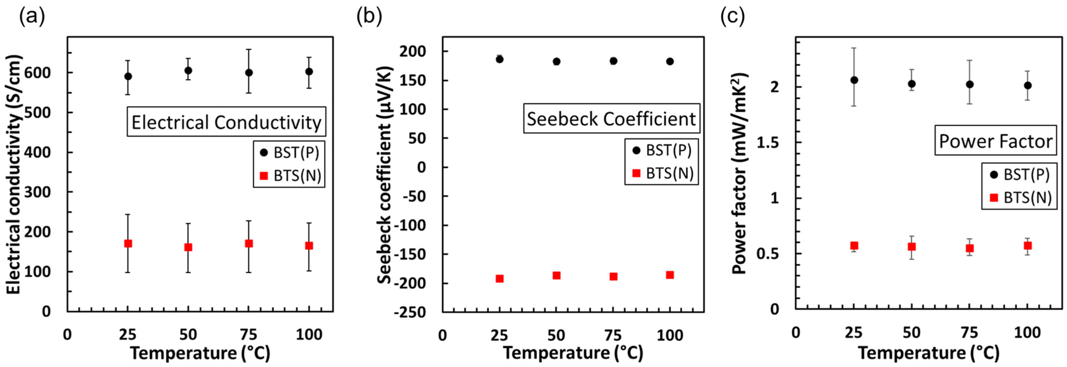
The results of the effect of temperature on the in-plane electrical conductivities and Seebeck coefficients of p-type chitosan-BST (1:2000 wt ratio) and n-type chitosan-BTS (1:2000 wt ratio) composite films are shown in Figure 3 [36,37,38,39]. These temperatures were chosen based on previous TEG studies focusing on low-waste heat applications [36,37,38,39]. The average electrical conductivity of the p-type chitosan-BST composite films (600 S/cm) was observed to be half of the bulk BST electrical conductivity (1200 S/cm) [11]. The average electrical conductivity (200 S/cm) of n-type chitosan-BTS composite films is also lower than bulk BTS (700–800 S/cm) [21]. The electrical conductivity depends on charge carrier concentration and carrier mobility. The decrease in the electrical conductivity of n- and p-type chitosan-TE composite films compared to their bulk counterparts can be attributed to a decrease in carrier mobility (μ). The carrier mobility is negatively affected by the presence of an insulating chitosan binder, which, when combined with the heterogeneous-sized TE particles, forms TE particle-chitosan interfaces and lowers the average mean free path of charge carriers due to the scattering at those interfaces. Additionally, forming pores or voids and gaps due to solvent evaporation and grain boundary interfaces in composite films contribute to carrier scattering, further reducing mobility and electrical conductivity [39].
The average electrical conductivity of n-type chitosan-BTS composite film was 200 S/cm, like previously reported n-type printed composite films [37,38,39]. Likewise, the average electrical conductivity of p-type chitosan-BST composite film at room temperature was 600 S/cm, comparable to previously reported p-type printed films [36,37,38,39]. However, using a nominal amount of chitosan binder (0.05 wt. %), we significantly reduced the insulating binder needed to print these composite films compared to the existing printed films [20]. Additionally, micron- and nanometer particles in the TE powder resulted in compact packing due to grain coalescence following hot pressing (applied pressure 200 MPa, curing at 200 °C for 30 min) [36,37,38,39].
As the temperature increased from 25 to 100 °C, the average electrical conductivity of p-type BST-100 composite films decreased from 600 S/cm to 500 S/cm, demonstrating the semi-metallic behavior of BST composite films [11,39]. In contrast, the average electrical conductivity of n-type BTS-100 composite films remained relatively stable as the temperature increased [37,38,39]. The electrical conductivity of TE composite films is a key factor in determining the resistance and power output of the TEG prototype.
The average value of the Seebeck coefficients of the n- and p-type composite films was between 190 and 200 µV/K. The n-type BTS composite film exhibited a negative Seebeck coefficient, which confirms its n-type behavior. In contrast, the p-type BST composite films display positive coefficients, indicating their p-type behavior. The average Seebeck coefficient of n-type and p-type composite films remained relatively stable from 25 to 100 °C [37,38,39]. The average Seebeck coefficient of n-type and p-type chitosan-based TE composite films is comparable to that of bulk and printed TE composite films [37,38,39]. The average power factor of p-type TE composite films was 2.04 mW/mK2, while the average power factor of n-type TE composite films was 0.56 mW/mK2. Because the average electrical conductivity of p-type BST-100 composite films is higher than that of n-type BTS composite films, the average power factor of p-type composite TE films is higher than that of n-type composite films. The power factors of the n-type and p-type TE composite films remained relatively stable up to 100 °C. The thermal conductivity of p-type BST composite film was 0.75 W/mK, and that of n-type BTS composite film was 0.56 W/mK at 25 °C [37,38,39]. The thermal conductivity of n-type BTS and p-type BST TE composite films was similar to that of our previously reported composite films prepared using cold pressing [37,38,39]. The average ZTs of p-type BST and n-type BTS composite films were 0.7 and 0.35 W/mK, respectively, making them some of the best-reported ZT values for printable TE films at 25 °C [36,37,38,39]. The stability of the electrical conductivity and Seebeck coefficient of TE composite films over the temperature range from 25 to 100 °C allows us to predict the suitability of a radial TEG device (made using n-type BTS-100 and p-type BST-100 composite inks) for various low-temperature waste heat applications.
3.3. Radial TEG Prototype Power Output Characterizations
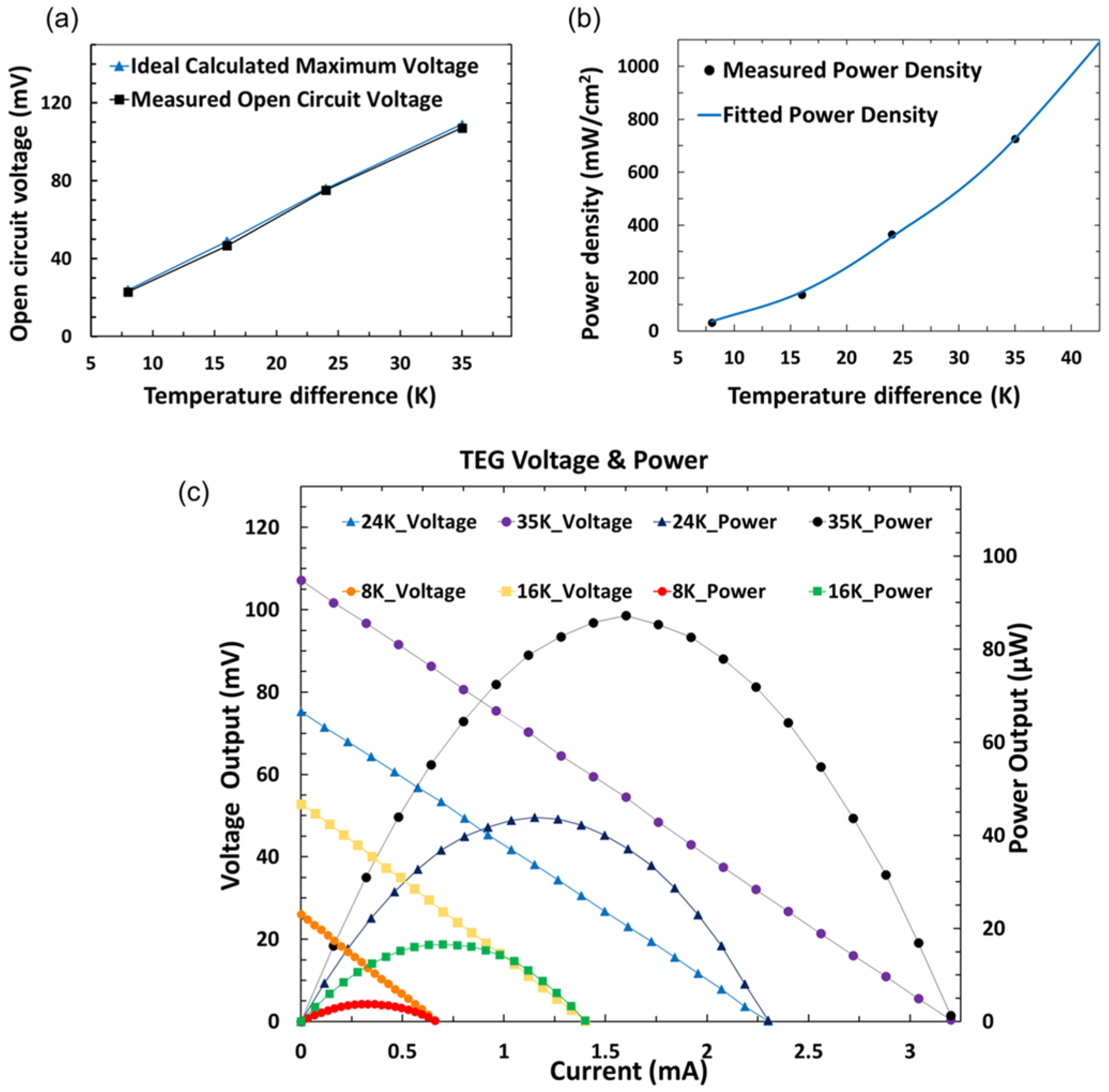
The seven-and-one-half couple radial TEG device fabricated using n-type chitosan-BTS-100 and p-type chitosan-BST-100 had a resistance of 34 Ω. Figure 4a shows the open-circuit voltage output of the radial TEG device measured at ΔT of 8, 16, 24, and 34 K. The maximum voltage was calculated using Equation (1):
where m is the number of n-type and p-type TE element couples in radial TEG device, αp is the absolute Seebeck coefficient of p-type TE composite film (average 200 µV/K), and αn is the absolute Seebeck coefficient of n-type TE composite film (average 190 µV/K). The calculated ideal and measured open-circuit voltage matched well even as ∆T increased (Figure 4a). The data indicate that the measured voltage increased linearly as ∆T increased. Figure 4b shows the power density of the TEG prototype and the fitted model power density. The power density is the measured power output per unit cross-sectional area of the TEG device. The fitted model power density was calculated using open-circuit voltage (Equation (1)), the resistance of the TEG device (RTEG, 34 Ω), and the area of the TEG device (ATEG) using Equations (2)–(4):
The cross-sectional area of the TEG device was calculated using Equation (3):
where ATEG is the total cross-sectional area, AT is the cross-sectional area of thermoelements, (width (2.5 mm) × thickness (0.16 mm) of the thermoelements), and AS is the cross-sectional area of spacing (between two thermoelements (2.0 mm) × thickness (0.16 mm). The power density was calculated using Equation (4):
The voltage and power output are plotted as a function of current at various ∆T (Figure 4c). The maximum power was obtained when the resistance of the TEG device was equal to the applied resistance. The maximum power output of 87 µW was obtained when the open-circuit voltage was half its original value (55 mV), and the current was 1.6 mA at a ∆T of 35 K. Therefore, the radial TEG device’s power output was sufficient to meet the average power requirements (10 µW–100 mA) of various condition monitoring sensor network devices used around heated pipes [6,7,8].
Figure 4.
Characterization results of a 7.5 radial TEG prototype: (a) ideal and measured open-circuit voltage vs. ΔT, (b) ideal and measured power density at various ΔT, and (c) TEG voltage and power curve at various ΔT.
Figure 4.
Characterization results of a 7.5 radial TEG prototype: (a) ideal and measured open-circuit voltage vs. ΔT, (b) ideal and measured power density at various ΔT, and (c) TEG voltage and power curve at various ΔT.

Table 1.
Performance of the prototype radial stencil-printed TEG device and other reported printed TEGs.
Table 1.
Performance of the prototype radial stencil-printed TEG device and other reported printed TEGs.
| Number of Couples | Dimensions | Resistance (Ω) | ΔT (K) | Max. Voltage (mV) | Max. Power (μW) | Power Density (μW/cm2) | Curing Temp (K) | Max. Curing Time (min) | Reference |
|---|---|---|---|---|---|---|---|---|---|
| 10 | 20 mm × 20 mm × 70 µm | 192 | 48 | 68 | 6 | 238 | 523 | 480 | [16] |
| 5 × 10 planar | 3.5 mm × 0.6 mm × 100 µm | 55 | 20 | 88 | 33 | 280 | 523 | 180 | [20] |
| 4 single leg | 10 mm × 2.7 mm × 27 µm | 8.5 | 80 | 60 | 54 | 1880 | 723 | 136 | [23] |
| 10 circular | 5 mm × 1.5 mm × 120 µm | 100 | 70 | 230 | 130 | 1230 | 523 | 360 | [25] |
| 9 planar | 6.5 mm × 2.3 mm × 150 µm | 12 | 40 | 54 | 73 | 566 | 393 | 60 | [36] |
| 2 single legs | 6 mm × 3 mm × 170 µm | 9 | 12 | 4.2 | 0.48 | 393 | 30 | [37] | |
| 3 single legs | 5 mm × 7 mm × 70 µm | 3 | 38 | 20 | 58 | 5720 | 423 | 30 | [38] |
| 6 | 7 mm × 3 mm × 170 µm | 5.9 | 40 | 90 | 357 | 5000 | 423 | 30 | [39] |
| 24 | 40 mm × 80 mm × 300 µm | 1600 | 35 | 10 | 0.015 | - | 393 | 30 | [40] |
| 7.5 radial | 7 mm × 2.5 mm × 160 µm | 37 | 34 | 110 | 87 | 727 | 393 | 60 | This work |
The calculated power density and the fitted model power density of the prototype were similar at all ∆T (8, 16, 24, and 35 K). The maximum power density of the actual prototype was 727 μW/cm2. The printed n-BTS and p-BST radial TEG device achieved 30% higher power density than our previous n-Bi and p-BST planar TEG device [36,37]. In this work, we used a low thermal budget and fast curing method to fabricate the radial TEG device that achieved power densities comparable to those of other printable TEG devices (Table 1). It is easy to fabricate a scalable TEG device by printing the desired number of thermoelements of any aspect ratio. The unique features of our prototype radial TEG device show that: (1) These devices can be easily stencil printed and are scalable, (2) unlike traditional rigid devices where thermoelements occupy lots of space, sufficiently large power output will be produced by packing a large number of high-aspect-ratio thermoelectric elements in a small and or multiple device, (3), the technology does not involve any high-temperature (500 °C) and long-duration (up to 18 h) processing. Developing a low thermal budget manufacturing method reduced energy use in production and enabled large-scale, production-worthy technology to fabricate TEGs. (4) These radial TEGs can be printed on a flexible Kevlar substrate and, therefore, can be used to harvest waste heat from hot pipes. Every electric energy captured from waste heat or saved through improved industrial heating is a kWh that does not have to be produced by burning fossil fuels, i.e., total energy efficiency has positive feedback on all energy realms and sustainability [41].
The characteristics of our radial TEGs may contribute to the development of self-sufficient power supplies for WSN devices. Radial TEG devices can be wrapped around hot water and steam pipes to harvest waste heat and convert it into usable energy for monitoring sensors that measure temperature, pressure, or steam leakage [13,14]. The obtained power output is sufficient to power various WSN modules that could be used in various condition monitoring devices around the waste heat pipes.
Developing printable and scalable TEG devices may offer a safe and sustainable alternative to current rigid and flammable battery systems for meeting the power needs of condition monitoring sensors used in various industrial applications. Future work will focus on developing the process parameters to fabricate more TEGs and engineering methods to wrap radial TEGs around waste heat pipes to harvest valuable electrical energy.
4. Conclusions
In this work, we used p-type BST and n-type BTS TE materials with a wide distribution of particle sizes (a combination of micro- and nanometer-sized particles) to create compact TE composite films and TE elements for TEG devices. The composites were cured via hot pressing at 200 MPa for 30 min at 200 °C. The chitosan binder (0.05 wt. %) held the particles in the TE composite films. The synergistic effect of the chitosan binder, a combination of micro- and nanometer-sized TE particles, and hot pressing (using a low-energy-input method) resulted in ZT values of 0.35 for the n-type and 0.7 for the p-type TE composite films. These values are comparable to the best-reported values for printed TE composite films. Our radial TEG prototype was stencil printed using p-type and n-type TE composite inks on gold-coated copper electrodes on a Kevlar substrate. The prototype generated a maximum power of 87 μW and a 727 μW/cm2 power density. Our radial TEG prototype’s power output and density are sufficient to power various condition-monitoring wireless sensor devices around heated pipes. One of the main highlights of our work is that we used an energy-efficient fabrication method to achieve power output and power density values for our radial TEG devices that are comparable to the best-reported values for printed TEG devices without the need for an energy-intensive curing method. Using cost-effective printing techniques and energy-efficient curing will contribute to the sustainable manufacturing of large-scale adoption of TEG devices.
Author Contributions
This work was proposed and coordinated by D.M., E.J. and P.B. conducted all the experiments and thermoelectric characterizations under the supervision of D.M. All experiments were performed in D.M.’s lab at UMBC. R.B.A. performed SEM characterizations. E.J. wrote the manuscript. D.M., L.D.T.T. and R.B.A. helped revise the manuscript. All authors have read and agreed to the published version of the manuscript.
Funding
This work was supported by Deepa Madan funds from the National Science Foundation award CMMI-2238996 and TEDCO-Maryland Innovation Initiative. Rohan B. Ambade would like to acknowledge the funding support from Advanced Research and Innovation Center (ARIC), which is jointly funded by STRATA Manufacturing PJSC (a Mubadala company), Department of Aerospace Engineering, Khalifa University of Science and Technology, and Sandooq Al Watan under Grant SWARD-S22-015.
Informed Consent Statement
No human study was involved.
Data Availability Statement
The data that support the findings of this study are available from the corresponding author upon reasonable request.
Acknowledgments
The authors thank Preetham Gowni (High school student) for creating the Matlab program to automate device testing setup. The authors would like to thank Jiyuan Huang, Luana Rojas Zurita, Yafet Mebrahtu, and Berchie Kubi for their contributions to helping perform various TE characterizations.
Conflicts of Interest
The authors declare that they have no known competing financial interests or personal relationships that could have appeared to influence the work reported in this paper.
References
- Filipponi, L.; Vitaletti, A.; Landi, G.; Memeo, V.; Laura, G.; Pucci, P. Smart City: An event driven architecture for monitoring public spaces with heterogeneous sensors. In Proceedings of the Fourth International Conference on Sensor Technologies and Applications, SensorComm 2010, Venice, Italy, 18–25 July 2010; IEEE Computer Society: Washington, DC, USA, 2010; pp. 281–286. [Google Scholar]
- Kocakulak, M.; Butun, I. An overview of Wireless Sensor Networks towards internet of things. In Proceedings of the IEEE 7th Annual Computing and Communication Workshop and Conference (CCWC) 2017, Las Vegas, NV, USA, 9–11 January 2017; 2017; pp. 1–6. [Google Scholar]
- Lazarescu, M.T. Design of a WSN platform for long-term environmental monitoring for IoT applications. IEEE J. Emerg. Sel. Top. Circuits Syst. 2013, 3, 45–54. [Google Scholar] [CrossRef]
- Akhtar, F.; Rehmani, M.H. Energy replenishment using renewable and traditional energy resources for sustainable wireless sensor networks: A review. Renew. Sustain. Energy Rev. 2015, 45, 769–784. [Google Scholar] [CrossRef]
- Guan, M.; Wang, K.; Xu, D.; Liao, W.H. Design and experimental investigation of a low-voltage thermoelectric energy harvesting system for wireless sensor nodes. Energy Convers. Manag. 2017, 138, 30–37. [Google Scholar] [CrossRef]
- Baldwin, R.; Bobovych, S.; Robucci, R.; Patel, C.; Banerjee, N. Gait analysis for fall prediction using hierarchical textile-based capacitive sensor arrays. In Proceedings of the 2015 Design, Automation & Test in Europe Conference & Exhibition 2015, Grenoble, France, 9–13 March 2015; EDA Consortium: San Jose, CA, USA, 2015; pp. 1293–1298. [Google Scholar]
- Chee, Y.-H.; Koplow, M.; Mark, M.; Pletcher, N.; Seeman, M.; Burghardt, F.; Steingart, D.; Rabaey, J.; Wright, P.; Sanders, S. PicoCube: A 1 cm3 sensor node powered by harvested energy. In Proceedings of the DAC 0‘8: The 45th Annual Design Automation Conference 2008, Anaheim, CA, USA, 8–13 June 2008; Association for Computing Machinery: New York, NY, USA, 2008; pp. 114–119. [Google Scholar]
- Milenković, A.; Otto, C.; Jovanov, E. Wireless sensor networks for personal health monitoring: Issues and an implementation. Comput. Commun. 2006, 29, 2521–2533. [Google Scholar] [CrossRef]
- Roundy, S.; Wright, P.K.; Rabaey, J. A study of low level vibrations as a power source for wireless sensor nodes. Comput. Commun. 2003, 26, 1131–1144. [Google Scholar] [CrossRef]
- Poudel, B.; Hao, Q.; Ma, Y.; Lan, Y.; Minnich, A.; Yu, B.; Yan, X.; Wang, D.; Muto, A.; Vashaee, D.; et al. High-thermoelectric performance of nanostructured bismuth antimony telluride bulk alloys. Science 2008, 320, 634–638. [Google Scholar] [CrossRef] [PubMed]
- Bell, L.E. Cooling, heating, generating power, and recovering waste heat with thermoelectric systems. Science 2008, 321, 1457–1461. [Google Scholar] [CrossRef]
- Park, S.H.; Jo, S.; Kwon, B.; Kim, F.; Ban, H.W.; Lee, J.E.; Gu, D.H.; Lee, S.H.; Hwang, Y.; Kim, J.-S.; et al. High-performance shape-engineerable thermoelectric painting. Nat. Commun. 2016, 7, 13403. [Google Scholar] [CrossRef]
- Park, J.W.; Kim, C.S.; Choi, H.; Kim, Y.J.; Lee, G.S.; Cho, B.J. A Flexible Micro-Thermoelectric Generator Sticker with Trapezoidal-Shaped Legs for Large Temperature Gradient and High-Power Density. Adv. Mater. Technol. 2020, 5, 2000486. [Google Scholar] [CrossRef]
- Kim, F.; Kwon, B.; Eom, Y.; Lee, J.E.; Park, S.; Jo, S.; Park, S.H.; Kim, B.S.; Im, H.J.; Lee, M.H.; et al. 3D printing of shape-conformable thermoelectric materials using all-inorganic Bi2Te3-based inks. Nat. Energy 2018, 3, 301–309. [Google Scholar] [CrossRef]
- Liu, K.; Tang, X.; Liu, Y.; Xu, Z.; Yuan, Z.; Zhang, Z. Enhancing the performance of fully-scaled structure-adjustable 3D thermoelectric devices based on cold–press sintering and molding. Energy 2020, 206, 118096. [Google Scholar] [CrossRef]
- Yuan, Z.; Tang, X.; Xu, Z.; Li, J.; Chen, W.; Liu, K.; Liu, Y.; Zhang, Z. Screen-printed radial structure micro radioisotope thermoelectric generator. Appl. Energy 2018, 225, 746–754. [Google Scholar] [CrossRef]
- Jang, E.; Poosapati, A.; Jang, N.; Hu, L.; Duffy, M.; Zupan, M.; Madan, D. Thermoelectric properties enhancement of p-type composite films using wood-based binder and mechanical pressing. Sci. Rep. 2019, 9, 7869. [Google Scholar] [CrossRef]
- Glatz, W.; Muntwyler, S.; Hierold, C. Optimization and fabrication of thick flexible polymer based micro thermoelectric generator. Sens. Actuators A Phys. 2006, 132, 337–345. [Google Scholar] [CrossRef]
- Tanwar, A.; Lal, S.; Razeeb, K.M. Structural design optimization of micro-thermoelectric generator for wearable biomedical devices. Energies 2021, 14, 2339. [Google Scholar] [CrossRef]
- Madan, D.; Wang, Z.; Wright, P.K.; Evans, J.W. Printed flexible thermoelectric generators for use on low levels of waste heat. Appl. Energy 2015, 156, 587–592. [Google Scholar] [CrossRef]
- Choi, H.; Kim, S.J.; Kim, Y.; We, J.H.; Oh, M.W.; Cho, B.J. Enhanced thermoelectric properties of screen-printed Bi0.5Sb1.5Te3 and Bi2Te2.7Se0.3 thick films using a post annealing process with mechanical pressure. J. Mater. Chem. C 2017, 5, 8559–8565. [Google Scholar] [CrossRef]
- Kim, S.J.; We, J.H.; Cho, B.J. A wearable thermoelectric generator fabricated on a glass fabric. Energy Environ. Sci. 2014, 7, 1959–1965. [Google Scholar] [CrossRef]
- Varghese, T.; Dun, C.; Kempf, N.; Saeidi-Javash, M.; Karthik, C.; Richardson, J.; Hollar, C.; Estrada, D.; Zhang, Y. Flexible thermoelectric devices of ultrahigh power factor by scalable printing and interface engineering. Adv. Funct. Mater. 2019, 30, 1905796. [Google Scholar] [CrossRef]
- Choi, H.; Kim, Y.J.; Kim, C.S.; Yang, H.M.; Oh, M.W.; Cho, B.J. Enhancement of reproducibility and reliability in a high-performance flexible thermoelectric generator using screen-printed materials. Nano Energy 2018, 46, 39–44. [Google Scholar] [CrossRef]
- Madan, D.; Wang, Z.; Chen, A.; Winslow, R.; Wright, P.K.; Evans, J.W. Dispenser printed circular thermoelectric devices using Bi and Bi0.5Sb1.5Te3. Appl. Phys. Lett. 2014, 104, 013902. [Google Scholar] [CrossRef]
- Huang, J.; Li, H.; Kirksey, E.; Hoffman, C.; Jang, H.J.; Wagner, J.; Madan, D.; Katz, H.E. Promising Thermoelectric Properties of Commercial PEDOT: PSS Materials and their Bi2Te3 Powder Composites. J. Appl. Phys. 2019, 125, 125502. [Google Scholar] [CrossRef]
- Hossain, M.S.; Li, T.; Yu, Y.; Yong, J.; Bahkb, J.H.; Skafidasa, E. Recent advances in printable thermoelectric devices: Materials, printing techniques, and applications. RSC Adv. 2020, 10, 8421. [Google Scholar] [CrossRef]
- Zhang, B.; Sun, J.; Katz, H.E.; Fang, F.; Opila, R.L. Promising thermoelectric properties of commercial PEDOT:PSS materials and their Bi2Te3 powder composites. ACS Appl. Mater. Interfaces 2010, 2, 3170–3178. [Google Scholar] [CrossRef]
- Zeng, M.; Zavanelli, D.; Chen, J.; Javash, M.S.; Du, Y.; LeBlanc, S.; Snyder, G.J.; Zhang, Y. Printing thermoelectric inks toward next-generation energy and thermal devices. Chem. Soc. Rev. 2022, 51, 485–512. [Google Scholar] [CrossRef]
- Byun, S.H.; Kim, C.S.; Agno, K.-C.; Lee, S.; Li, Z.; Cho, B.J.; Jeong, J.-W. Design strategy for transformative electronic system toward rapid, bidirectional stiffness tuning using graphene and flexible thermoelectric device interfaces. Adv. Mater. 2021, 33, 2170076. [Google Scholar] [CrossRef]
- Lv, H.; Liang, L.; Zhang, Y.; Deng, L.; Chen, Z.; Liu, Z.; Wang, H.; Chen, G. A flexible spring-shaped architecture with optimized thermal design for wearable thermoelectric energy harvesting. Nano Energy 2021, 88, 106260. [Google Scholar] [CrossRef]
- Wang, X.; Liang, L.; Lv, H.; Zhang, Y.; Chen, G. Elastic aerogel thermoelectric generator with vertical temperature-difference architecture and compression-induced power enhancement. Nano Energy 2021, 90, 106577. [Google Scholar] [CrossRef]
- Liu, L.; Chen, J.; Liang, L.; Deng, L.; Chen, G. A PEDOT:PSS thermoelectric fiber generator. Nano Energy 2022, 102, 107678. [Google Scholar] [CrossRef]
- Du, C.; Cao, M.; Li, G.; Hu, Y.; Zhang, Y.; Liang, L.; Liu, Z.; Chen, G. Toward Precision Recognition of Complex Hand Motions: Wearable Thermoelectrics by Synergistic 2D Nanostructure Confinement and Controlled Reduction. Adv. Funct. Mater. 2022, 32, 2206083. [Google Scholar] [CrossRef]
- Li, G.; Hu, Y.; Chen, J.; Liang, L.; Liu, Z.; Fu, J.; Du, C.; Chen, G. Thermoelectric and Photoelectric Dual Modulated Sensors for Human Internet of Things Application in Accurate Fire Recognition and Warning. Adv. Funct. Mater. 2023, 33, 2303861. [Google Scholar] [CrossRef]
- Jang, E.; Banerjee, P.; Huang, J.; Madan, D. High performance scalable and cost-effective thermoelectric devices fabricated using energy efficient methods and naturally occurring materials. Appl. Energy 2021, 294, 117006. [Google Scholar] [CrossRef]
- Banerjee, P.; Jang, E.; Huang, J.; Holley, R.; Vadnala, S.; Sheikh, A.; Trivedi, A.; Jackson, K.; Homman, V.K.; Madan, D. Thermoelectric performance enhancement of n-type chitosan-Bi2Te2.7Se0.3 composite films using heterogeneous grains and mechanical pressure. J. Electron. Mater. 2021, 50, 2840–2851. [Google Scholar] [CrossRef]
- Banerjee, P.; Huang, J.; Ambade, R.B.; Jang, E.; Saeidi-Javash, M.; Zhang, Y.; Madan, D. Effect of particle-size distribution and pressure-induced densification on the microstructure and properties of printable thermoelectric composites and high energy density flexible devices. Nano Energy 2021, 89, 106482. [Google Scholar] [CrossRef]
- Huang, J.; Ambade, R.B.; Lombardo, J.; Brooks, B.; Poosapati, A.; Banerjee, P.; Javash, M.S.; Zhang, Y.; Madan, D. Energy Density Enhancement of Scalable Thermoelectric Devices Using a Low Thermal Budget Method with Film Thickness Variation. Appl. Mater. Today 2024, 37, 102116. [Google Scholar] [CrossRef]
- Lu, Z.; Zhang, H.; Mao, C.; Li, C.M. Silk fabric-based wearable thermoelectric generator for energy harvesting from the human body. Appl. Energy 2016, 164, 57–63. [Google Scholar] [CrossRef]
- Mamur, H.; Dilmaç, O.F.; Begum, J.; Bhuiyan, M.R.A. Thermoelectric generators act as renewable energy sources. Clean. Mater. 2021, 2, 100030. [Google Scholar] [CrossRef]
Figure 1.
Radial TEG device using chitosan p-BST and chitosan n-BTS (left-hand side).
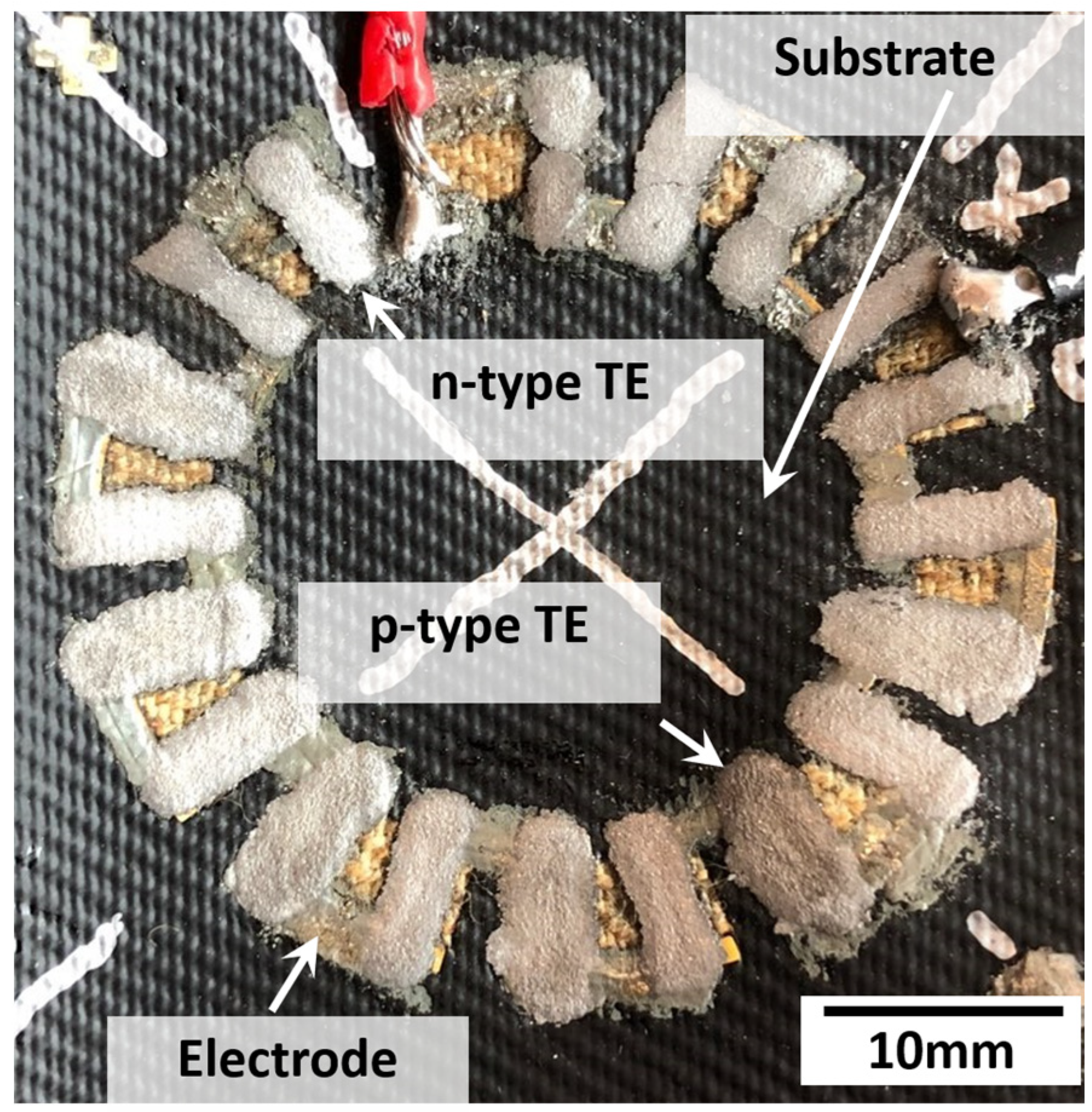
Figure 2.
XRD patterns of 100 mesh n-type BTS particles (top) and p-type BST particles (bottom).
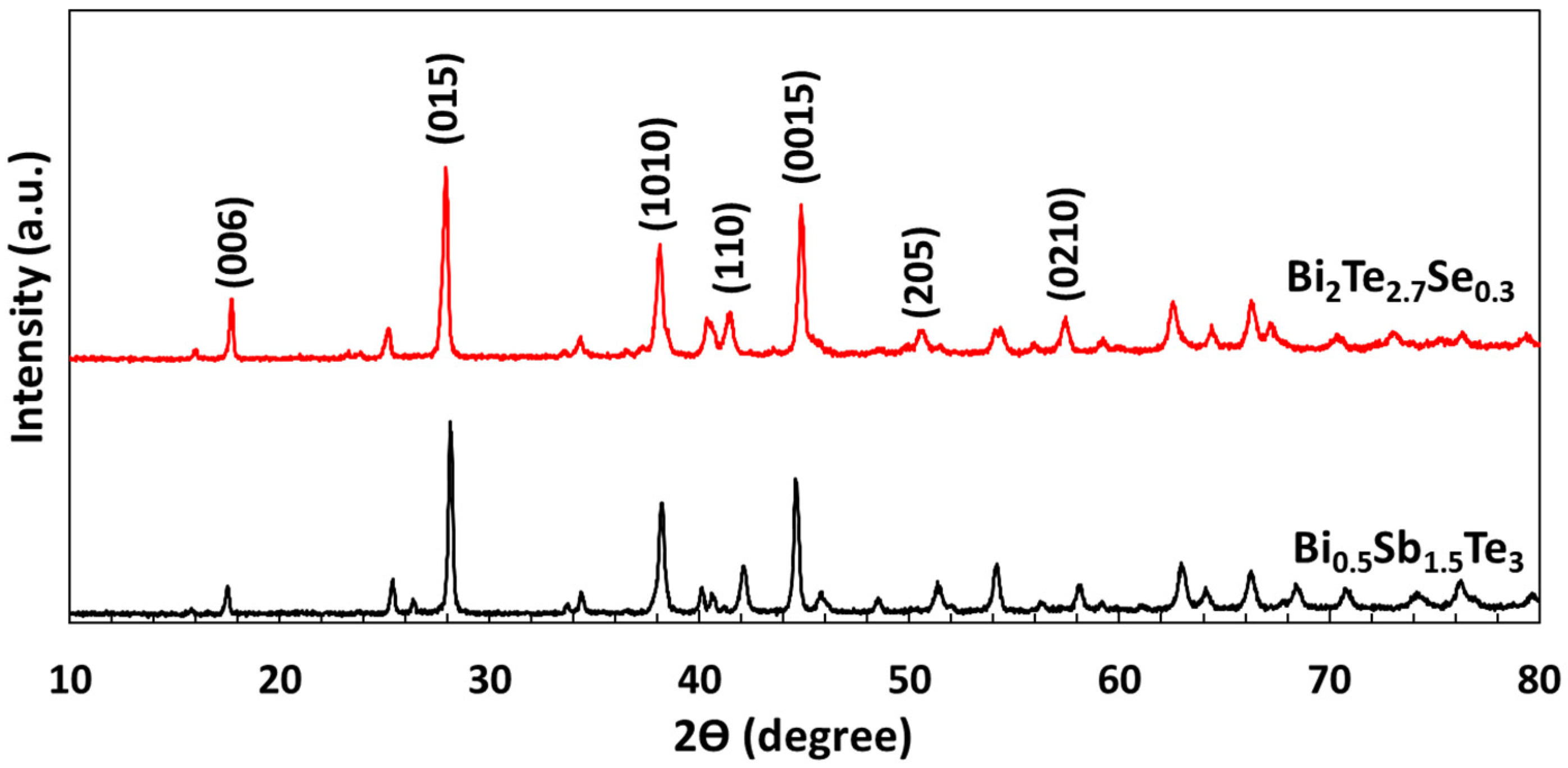
Figure 3.
(a) Electrical conductivity, (b) Seebeck coefficient, and (c) power factor of p-type chitosan-BST-100 and n-type chitosan-BTS-100 TE composite films (1:2000 wt. ratio, hot pressed at 200 MPa at 200 °C for 30 min) as a function of temperature from 25–100 °C.
Figure 3.
(a) Electrical conductivity, (b) Seebeck coefficient, and (c) power factor of p-type chitosan-BST-100 and n-type chitosan-BTS-100 TE composite films (1:2000 wt. ratio, hot pressed at 200 MPa at 200 °C for 30 min) as a function of temperature from 25–100 °C.
Disclaimer/Publisher’s Note: The statements, opinions and data contained in all publications are solely those of the individual author(s) and contributor(s) and not of MDPI and/or the editor(s). MDPI and/or the editor(s) disclaim responsibility for any injury to people or property resulting from any ideas, methods, instructions or products referred to in the content. |
© 2024 by the authors. Licensee MDPI, Basel, Switzerland. This article is an open access article distributed under the terms and conditions of the Creative Commons Attribution (CC BY) license (https://creativecommons.org/licenses/by/4.0/).
Share and Cite
MDPI and ACS Style
Jang, E.; Ambade, R.B.; Banerjee, P.; Topoleski, L.D.T.; Madan, D. Stencil-Printed Scalable Radial Thermoelectric Device Using Sustainable Manufacturing Methods. Sustainability 2024, 16, 3560. https://doi.org/10.3390/su16093560
AMA Style
Jang E, Ambade RB, Banerjee P, Topoleski LDT, Madan D. Stencil-Printed Scalable Radial Thermoelectric Device Using Sustainable Manufacturing Methods. Sustainability. 2024; 16(9):3560. https://doi.org/10.3390/su16093560
Chicago/Turabian StyleJang, Eunhwa, Rohan B. Ambade, Priyanshu Banerjee, L. D. Timmie Topoleski, and Deepa Madan. 2024. "Stencil-Printed Scalable Radial Thermoelectric Device Using Sustainable Manufacturing Methods" Sustainability 16, no. 9: 3560. https://doi.org/10.3390/su16093560
Note that from the first issue of 2016, this journal uses article numbers instead of page numbers. See further details here.