Investigation of 1200 V SiC MOSFETs’ Surge Reliability

1
School of Information & Electrical Engineering, Zhejiang University City College, Hangzhou 310015, China
2
College of Electrical Engineering, Zhejiang University, Hangzhou 310027, China
*
Author to whom correspondence should be addressed.
Micromachines 2019, 10(7), 485; https://doi.org/10.3390/mi10070485
Submission received: 10 May 2019
/
Revised: 11 July 2019
/
Accepted: 12 July 2019
/
Published: 18 July 2019
(This article belongs to the Special Issue Miniaturized Transistors, Volume II)
Abstract
:In this work, the surge reliability of 1200 V SiC metal-oxide-semiconductor field-effect transistors (MOSFETs) from various manufactures has been investigated in the reverse conduction mode. The surge current tests have been carried out in the channel conduction and non-conduction modes. The experimental results show that the maximum surge currents that the devices can withstand are similar for both cases. It is found that short circuits occurred between the gate and the source in the failed devices. The characteristics of the body diode have also changed after the tests. By measuring the device characteristics after each surge current is applied, it can be concluded that the damages to the gate oxide layer and the body diode occurred only when the maximum surge current is applied. By decapping the failed devices and observing the cross section of the damaged cell, it is found that high temperature caused by excessive current flow through the devices during the surge tests is the main reason for the device failure. Finally, the TCAD simulation of the devices has been carried out to bring insight into the operation of the devices during the surge events.
1. Introduction
For decades, silicon material has always been the main semiconductor material used to power electronic devices. However, the performance of silicon devices has approached its theoretical limit determined by the material characteristics. While various applications demand ever-increasing performance from power devices, silicon can no longer meet the requirements of high power, high frequency, high speed and high temperature. Therefore, more attention has been paid to power electronic devices based on wide bandgap semiconductor materials [1,2].
Compared with Silicon, wide bandgap semiconductors SiC, GaN and diamond have the advantages of wide bandgap, high thermal conductivity and high saturation speed. Due to their excellent performance, wide bandgap semiconductors are more suitable for high voltage, high temperature and high switching frequency applications [3,4]. While power devices based on diamond are still in the early research stage [5], some GaN and SiC products are already available in the commercial market. At present, commercial GaN devices are mainly high electron mobility transistors (HEMTs) rated 600 V and below [6,7]. On the other hand, SiC devices are more widely available in voltage ranges between 600 and 3300 V [8,9].
Although wide bandgap semiconductor materials have a lot of advantages, their high cost and poor reliability restrict their large scale commercialization. Current surges are common in the power electronics circuits. For example, the devices have to withstand several folds of the rated current during the startup process of a power factor correction (PFC) circuit or an inverter-fed motor drive. The maximum surge current that a device can withstand is usually referred to as its surge current capability. Excessive surge current will cause irreversible damage to devices, and continuous surge current will also have a negative impact on the device performance. Therefore, surge capability is an important parameter of devices requiring detailed investigation. Among the three wide bandgap semiconductors mentioned above, SiC devices are the most mature. At this point, metal-oxide-semiconductor field-effect transistor (MOSFET) is the SiC commercial product attracts the most attention. Therefore, in this work, surge capability of SiC MOSFETs has been studied.
Until now there have been a number of surge reliability studies of Si diodes [10] and insulated-gate bipolar transistors (IGBTs) [11,12,13]. Considerable research work about the surge reliability of SiC devices has also been carried out in recent years, but the results mainly focused on the reliability of SiC Schottky diodes [14,15,16,17]. On the SiC MOSFET, most reliability work has been carried on under short-circuit conditions. Some researchers have investigated the failure of SiC MOSFETs under short circuit and surge current conditions with a thermal model [18]. Some researchers have tested the maximum surge currents of 1200 V SiC MOSFETs’ body diodes under various conditions [19,20]. The test conditions were varied by changing temperatures, pulse width of surge currents, gate voltages and so on. Some have also compared the surge reliability of SiC MOSFET’s body diodes to those of other Si devices’ body diodes [21,22,23,24]. However, in these works only measurement results were presented. Analysis on the internal causes of the device failure has not been presented.
In this paper, the surge reliability of SiC MOSFETs operating in the reverse conduction mode has been studied. Firstly, several 1.2 kV SiC MOSFETs from several major manufactures has been tested in the channel conduction and non-conduction modes to get the maximum surge currents that the devices could withstand. The performance changes of devices after each surge test were checked to help to understand the process of the failure. In order to find out the failure mechanism, anatomy work has been done to two representative failed devices to identify the damages inside the devices. The results have been analyzed in depth. At last, TCAD simulation has been employed to obtain some insight into the operation of the devices during the surge events.
2. Materials and Methods
The SiC MOSFETs studied in this paper were vertical N- channel power MOSFETs with a planar gate structure. Shown in Figure 1 is the cell structure of the SiC MOSFET C2M0080120D from Cree Company (Durham, NC, USA). The drain electrode is located at the bottom of the device, in contact with the N+ substrate region. The source electrode and the gate electrode are located on the top of the device, separated by the interlayer insulator. The channel is located in the P− well region, between the N+ source region and the N− drift region. The P+/P− well regions and N− drift region form a PN junction, which is the body diode. The dimension of the regions inside the device has been obtained by SEM. The doping concentrations of the regions have been derived from the device characteristics and the dimension of the regions. The structure parameters of MOSFET are shown in Table 1.
2.1. The Reverse Conduction Characteristics of SiC Metal-Oxide-Semiconductor Field-Effect Transistor (MOSFET)
Until now, there have been a lot of studies on SiC MOSFETs’ body diodes. Their static characteristics are similar to those of the ordinary diodes [25,26,27,28].
In Figure 2a, the transfer characteristics of the SiC MOSFET C2M0160120D manufactured by Cree Company is measured to obtain the threshold voltage and plotted. It can be seen that the MOSFET has a threshold voltage of around 2.6 V. By changing the gate voltages, the reverse I-V curves of the device are tested and the results are shown in Figure 2b.
In the reverse conduction mode, there are two possible parallel current paths, namely, the body diode and the MOS channel. The body diode only turns on when the voltage across the P+ or P−well/N− drift junction exceeds its turn-on voltage (approx. 2.7 V under room temperature), which explains the I-V curve with Vgs = −5 V in Figure 2b. On the other hand, when reverse-biased, the MOS channel opens when Vgd exceeds Vth and current flows from source to drain. This explains the I-V curves with Vgs = 5 V to 20 V where the reverse current of the device increases starting from Vsd = 0 V. When Vgs = 0 V, the MOS channel starts reverse conducting at Vsd = 2.6 V and the body diode starts conducting at Vsd = 2.7 V, which gives an I-V curve very similar to that of Vgs = −5 V [29]. It is also interesting to note that, for Vgs = 5 V to 20 V, the I-V curves start to bend upwards when Vsd exceeds 3 V. This is because of the addition of the body current to the existing MOS current. Once turned-on, the current in the body diode increases exponentially with voltage. As a result, the body diode becomes the main conducting path with further increase of the bias voltage.
2.2. Setup of the Surge Current Tests
The simplified schematic of the surge current reliability test circuit is shown in Figure 3. To test the surge reliability of the device-under-test (DUT), this circuit is operated in the following steps. Firstly, S1 is closed and S2 remains open. The voltage source V1 charges the capacitor C. Then, S1 is open and S2 is closed. The charge stored in capacitor C is discharged through the DUT (M1) and the inductor L. A large instantaneous current flows through the DUT. The LC oscillation circuit is used to generate a sinusoidal surge current. The period of the current was determined by the inductance L and capacitance C, which could be expressed as:
In the tests, the sinusoidal current period is set as 20 ms [30]. The values of C and L are chosen as: C = 2 mF, L = 5 mH to satisfy the equation. The magnitude of the sinusoidal current is determined by the following formula:
in which U is the voltage of V1 and I is the amplitude of the sinusoidal current flowing through the DUT. During the tests, the amplitude of the surge current is increased gradually by adjusting voltage source V1.
In this experiment, 1200 V SiC MOSFETs from several major manufacturers were selected for testing. They were C2M0080120D and C2M0160120D from Cree, SCT3160KLGC11 from ROHM (Kyoto, Japan), SCT10N120 from STM (Geneva, Switzerland) and LSIC1MO120E0160 from Lifflefuse (Chicago, IL, USA). The major parameters for the tested devices have been listed in Table 2.
All the devices mentioned above were tested under the reverse conduction state. A half-wave sinusoidal current pulse with a pulse width of 10 ms was used. The amplitude of the current was increased gradually until the device failed. After each test, the device was cooled down to the room temperature before the next test started, so as to prevent the heat generated in the device from affecting the results of the subsequent tests. The surge failure of the device could be determined by observing the distortion of the voltage Vds.
The maximum surge current capability of each device was obtained from the tests. The tests have been carried out in the channel conduction and non-conduction modes. Therefore, two gate-source voltage biases, 10 V and −3 V, were applied respectively. For every device type and each test condition, three samples were tested.
After the device failed, the static characteristics were measured and compared to the characteristics obtained before the surge currents were applied. These measurements include the transfer characteristic, the reverse I-V characteristics and the resistance between electrodes.
3. Results
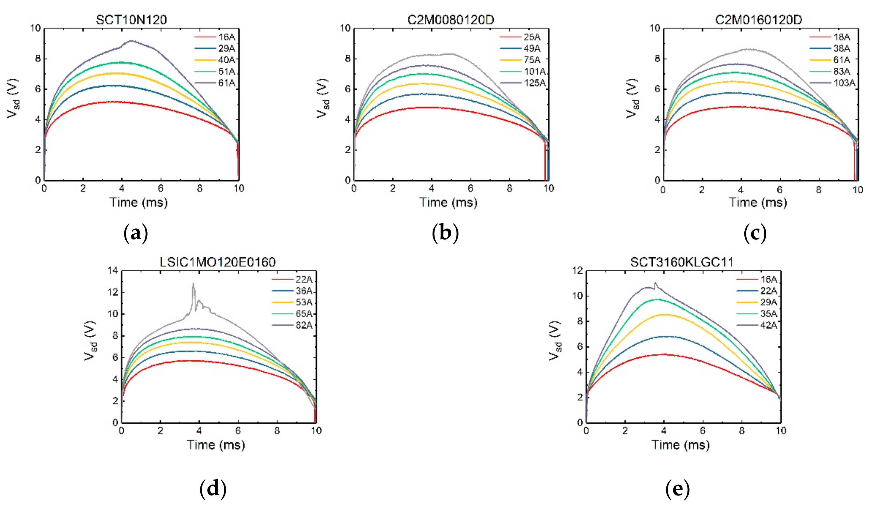
In Figure 4, Vgs is set to −3 V. It can be seen that initially there is a sudden rise in the voltage curve. Since with Vgs = −3 V, the current largely flows through the body diode region. The magnitude of the sudden rise corresponds to the on-set voltage of the body diode. Then the voltage increases accordingly with the current. However, it can be seen that the peak of the voltage does not occur when the current reaches its peak value (which is at 5 ms for a 20 ms-period sinusoidal current waveform). It is because in the bipolar mode, the device has a negative temperature coefficient. During each test pulse, as the device is continuously heated up, the voltage peak appears somewhat earlier than the current peak.
In Figure 5, Vgs is set to 10 V. Initially there is no sudden rise of the voltage, since the channel is turned on and it carries all the current. When the voltage Vsd exceeds the on-set voltage of the body diode (~2.7 V), the slope of the voltage curve changes as the body diode starts to conduct. Comparing Figure 4 and Figure 5, the maximum surge currents of the SiC MOSFETs’ in channel conduction and non-conduction modes are very close to each other. This is due to the fact that at Vsd of 6 V and higher (with a likely high junction temperature), the body diode is operating in a bipolar mode with heavy conductivity modulation, making it the dominant current path against the MOS channel. Therefore, whether the channel is conducting or not does not significantly impact the surge current capability of the device. It is also found that the device failure occurs at the time of 3.5 ms in both cases.
The maximum surge currents that the devices can withstand are listed in Table 3. It can be seen that in general the maximum surge current is about 5 times of rated current.
4. Discussion
4.1. Analysis of Test Result
4.1.1. Comparison of Devices’ Characteristics before and after the Surge Reliability Tests
In this section, the characteristics of the failed MOSFETs have been measured and summarized. According to their behaviors after the tests, the devices can be classified into two groups: The devices in the first group cannot block the reverse voltage anymore, while the devices in the other group still have the reverse voltage blocking capability. Therefore, the following work focuses on two devices representing these two cases respectively: SCT10N120 from STM and C2M0160120D from Cree.
The first failure phenomenon is the short circuit between the gate and the source. During the test, it was found that when the failure occurred, the gate-source voltage dropped to 0 V and a bias voltage could not be applied to the gate. It was preliminary judged that the short circuit occurred between the gate and the source. Therefore, the resistances between the electrodes of MOSFETs before and after the surge failure were tested and shown in Table 4. It can be seen that the resistances before the surge tests are very large and out of the measurement range of the digital multimeter. However, the resistances between the gate and the source of the damaged devices are less than 1 Ω, indicating that the gate is short circuited to the source. In addition, Rds of the device SCT10N120 after the test is 14 kΩ, which means that damage has also occurred in regions between the drain and the source.
The second abnormal behavior is that the performance of the body diode has changed. In Figure 6 and Figure 7, the forward I-V and reverse blocking characteristics of the failed devices were measured and compared against those before failure.
As shown in Figure 6, for some devices represented by SCT10N120 (STM), the performance of the body diode has changed significantly after the tests, while the devices represented by C2M0160120D (Cree) was not damaged as badly as SCT10N120 (see Figure 7). For both devices, the forward voltage drops of the body diodes have decreased, but the voltages of Cree’s device were reduced less. In terms of the reverse blocking capability, the difference is more significant. Device SCT10N120 has completely lost its reverse blocking capability. However, the Cree device C2M0160120D still exhibits excellent reverse blocking capability.
4.1.2. Static Characteristic Variation of the Tested Device
In the sections above, the results of the surge reliability tests and the behaviors of the failed devices have been presented and summarized. However, device failure did not necessarily occur at the test the maximum surge current was applied. The damage might have accumulated when the surge current was increased gradually. To help to understand the process of the failure and find out the failure mechanisms of the devices, the characteristics of the devices have been measured after every surge current was applied.
The damage of SiC MOSFETs usually occurs in the gate oxide layer, so it is necessary to observe the change of the gate oxide layer’s characteristics. Whether the gate oxide layer is damaged or not can be observed from the change of the transfer curves. Thus, the transfer characteristics have been measured with Vds = 10 V. The sub-threshold swing is a performance index to measure the switching rate [31]. It is closely related to the interface trap density of gate oxide layer. It represents the variation of the gate voltage required for a ten-fold change in the drain current when the device is operating in the sub-threshold region. It is also called S factor. Smaller S factor corresponds to faster switching rate. It can be calculated from the following equation:
The sub-threshold swing is related to the interface trap density Dit, as shown in the following equation:
Hence the change of the interface trap density can be derived from the change of sub-threshold swing. In turn the state of gate oxide layer can be deduced by observing the change of the sub-threshold swing characteristics. The results have been measured and shown in Figure 8 and Figure 9. Also included are the forward conduction characteristics of the body diode in which Vgs is set to −3 V to keep the channel off.
It can be seen from the figures that even applying a surge current very close to the maximum surge current the static characteristics of the devices remain nearly unchanged. Hence it can be concluded that the damages to the gate oxide layer and the body diode occurred only at the time the maximum surge current was applied.
4.2. Analysis of Failure Mechanism
During a surge event, the junction temperatures inside the semiconductor devices can reach extremely high values, possibly several times the maximum rated temperature. It was reported that the main failure mechanism for standard silicon diode and transistor chips within module housings, is the melting of the anode-side metallization [32,33,34].
To investigate the failure mechanisms of these tested SiC MOSFET devices, anatomy work has been carried out. The following two devices were examined, namely, SCT10N120 (STM) and C2M0160120D (Cree). The anatomical results of the damaged devices are shown in Figure 10 and Figure 11.
Figure 10a is the image of the decapped STM device SCT10N120. The burn mark of the device is very obvious. Removing the layers to the substrate, there is still apparent damage in the substrate layer (Figure 10b). The burned area is concentrated near the bonding wires, indicating that the burnout was caused by the excessive current flowing through the bonding wires.
Figure 11a is the image of the decapped Cree device C2M0160120D. There are also severe burn marks. Compared with the results of SCT10N120, the burn areas of Cree device are more uniform and the degree of burn is lighter. It was found that the Cree device has more bonding wires (four wires) than the STM device (one wire). Therefore, it is possible that multiple bonding wires can spread out current, thus lower the maximum junction temperature and improve the surge performance of devices.
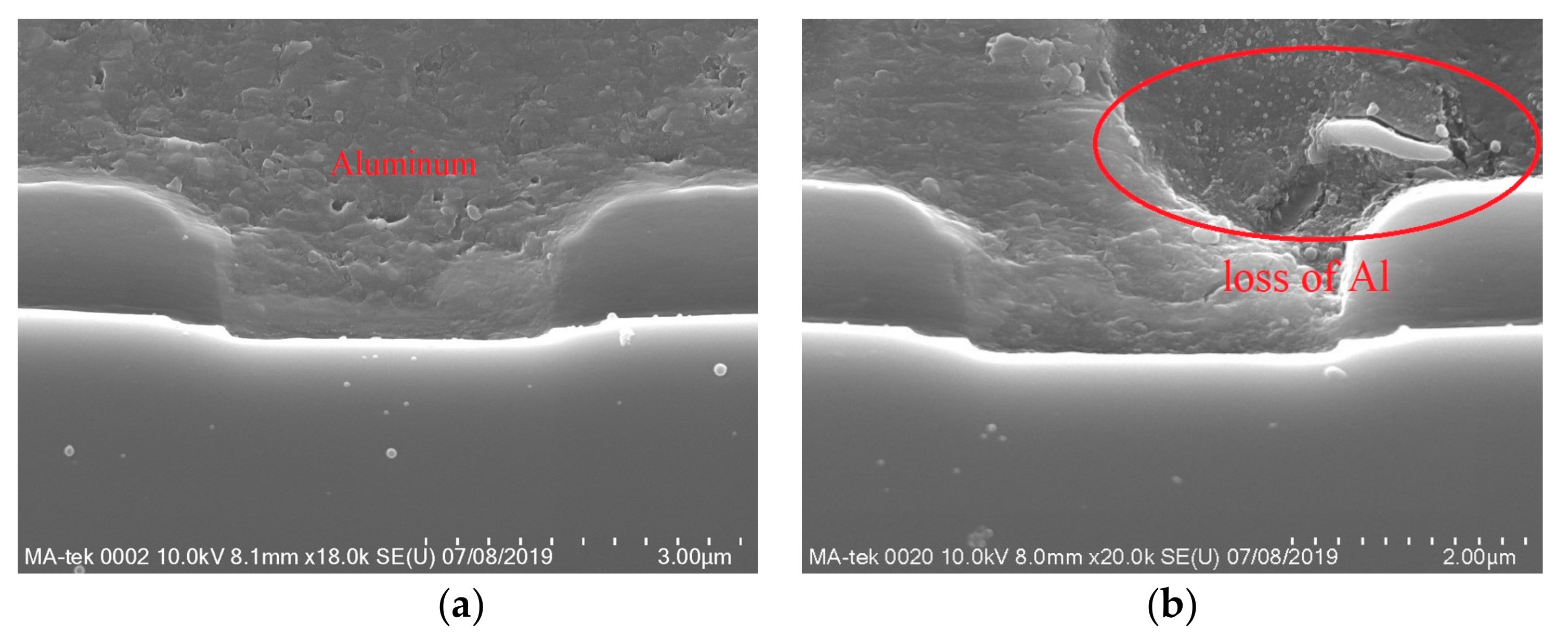
In addition, it is found that the melted Al covers the gate, as marked in the figures. This indicates that Al might have penetrated into the gate and causing the short circuit between the gate and the source.
From the anatomical results, the high temperature caused by excessive current is the main reason for the device failure. The high temperature caused burnout in many areas inside the device and eventually led to the device failure. In order to understand the process of the failure more clearly, the cross section of the damaged cell was cut and observed by SEM. The results are shown in Figure 12 and Figure 13.
Device SCT10N120 has been damaged more severely than device C2M0160120D. By comparing the SEM images of SCT10N120 taken before and after the failure, a few different types of device damages are possible.
4.2.1. Aluminum Melted and Diffused into the Interlayer Dielectric
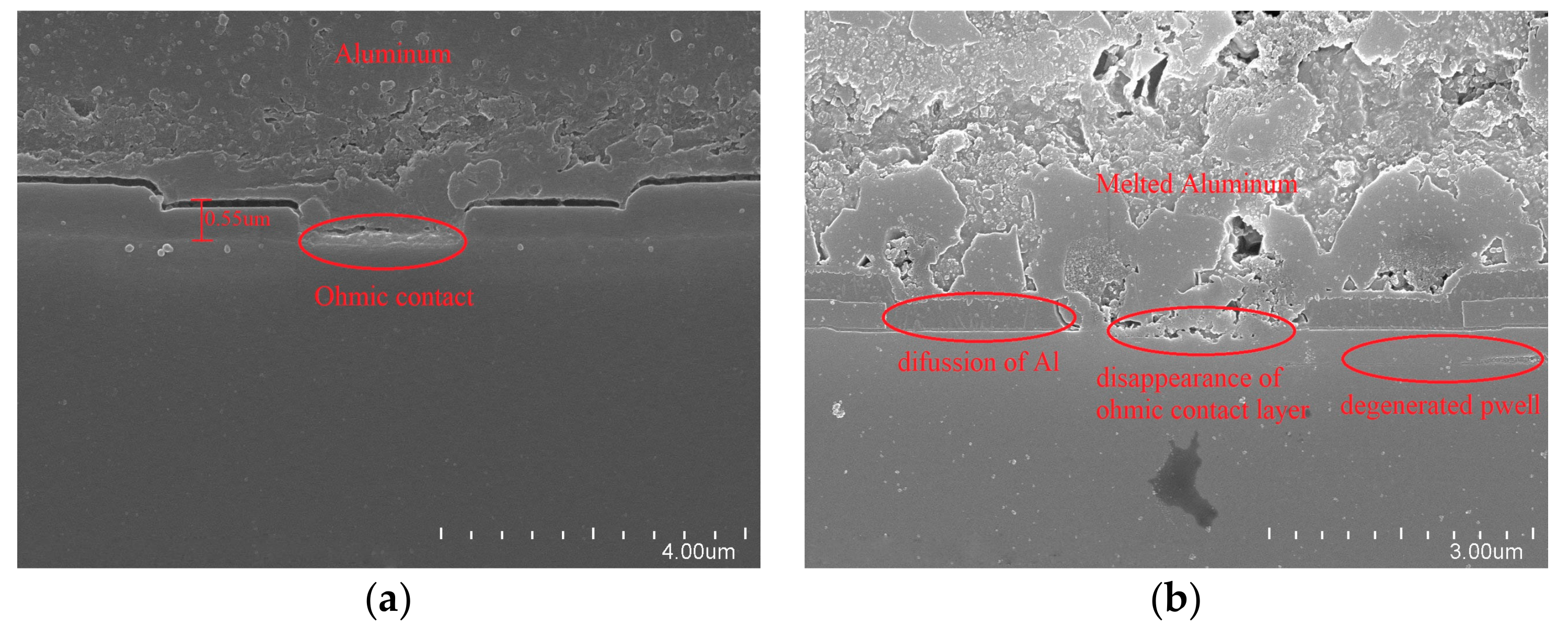
Aluminm (Al) is used to form electrodes in these devices. Firstly, it is observed that Al was melted inside the failed devices. Secondly, it is found that the interlayer dielectric became thinner and its depth is changed from 0.55 µm to 0.36 µm, which indicates that Al may has eroded the interlayer dielectric.
A high temperature can melt Al which could diffuse into the insulator and cause the short circuit of the gate and source. The process is described by the following equation:
As mentioned in some literature, the product of the above reaction, Si, rapidly dissolves or migrates into Al, leaving fine voids, ()Al2O3, in Al2O3.
Then, Al will self-diffuse into the voids and fills them,
where (Al)Al2O3 represents the Al that occupies the Al2O3 voids. Thus, the Al can react again with fresh SiO2 (silicate glass) at the bottom of the Al2O3 voids in the process described by Equation (6) [35,36,37].
In addition, white spots appeared in the interlayer dielectric, indicating that Al has diffused into the interlayer dielectric. It also caused the short circuit of the gate and source.
4.2.2. Ohmic Contact Layer Disappeared
As shown in Figure 12a, there is an ohmic contact layer between the source metal and N+ source area. In Figure 12b, this ohmic contact layer disappears and the boundary between the source metal and N+ source area disappears.
For NMOS, Ni is generally used as an ohmic contact material [38,39]. The ohmic contact layer is formed by rapid annealing at high temperature after the deposition. Because Ni can easily react with SiC to form silicide at high temperature, NiSi and Ni2Si are the main components in the ohmic contact layer.
Previously Hökelek and Robinson reported that Al started to react with NiSi at 400 °C by decomposing it and forming NiAl3 and Si [40], as shown in the following equation:
In reference to the findings of Bartur and Nicolet [41], the disappearance of Ni2Si can be described as the result of an alternate process consisting of the thermodynamically feasible reaction:
The eutectic reaction of Si and Al (Equation (9)) enables Al to react with the ohmic contact layer continuously, eventually lead to the disappearance of the ohmic contact layer.
4.2.3. Al Penetrated into SiC
The ohmic contact layer can prevent contact between Al and SiC. However, with the disappearance of the ohmic layer, Al penetrated into SiC regions. In Figure 12b, there is a discontinuous white line at 0.42 µm below the gate showing that Al has penetrated into the device. It is located at the boundary between the Pwell region and the N- drift region. It would affect the contact barrier of the body diode. Thus, the blocking performance of body diode would be affected.
In comparison, device C2M0160120D only exhibits the loss of Al, indicating Al has melted during the test. However, no penetration of Al into SiC regions has been found. That explains why the body diode of C2M0160120D can still have the reverse blocking capability after the test.
Therefore, the above analysis further reveals the failure regions and mechanisms of the device. When a large surge current flowed into the device, the device quickly heated up. The metal of the source electrode melted, eroded the interlayer dielectric then made the gate and the source contact each other. This eventually led to the short circuit between the gate and the source. Furthermore, the melted Al penetrated into the ohmic contact layer and made the ohmic contact layer disappear. Penetration of the Al into the body diode P/N junction also compromises its blocking capability.
4.3. Analysis of Simulation Result
In order to verify the findings of the experiments, finite element numeric simulation of the device has been carried out.
4.3.1. Simulation Setting
The simulation was completed by Silvaco TCAD, the device structure was generated by Devedit, and the surge simulation was completed by Mixmode. The structure of the SiC MOSFET C2M0080120D is shown in Figure 1. The structure parameters of the device are listed in the Table 1. The physical models used in simulation are shown in Table 5.
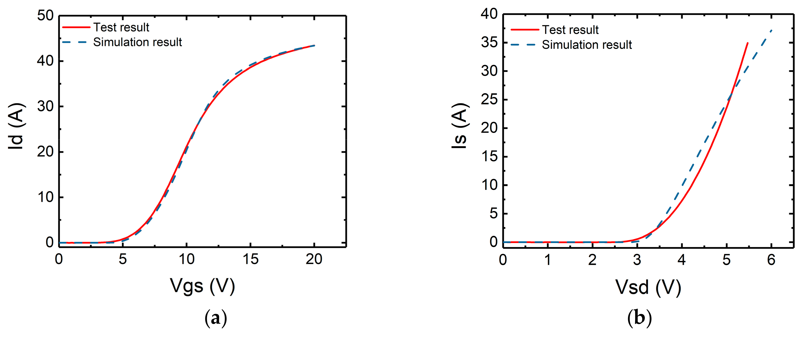
To verify the simulation setting, the transfer characteristic of the device has been simulated and compared with the experimental results in Figure 14a. It can be seen that the curves match each other. Also shown in Figure 14b is the simulation and experimental results of the body diode forward conduction characteristics. The results are very similar.
4.3.2. Surge Simulation Results and Analysis
Based on the device structure parameters listed in Table 1, the device was simulated and results were obtained. The input current was a sinusoidal current, with a 20 ms period.
The Channel Non-Conducting Mode
Atlas is not capable of directly simulate the device failure discussed in the previous sections, as it is mainly caused by some chemical reactions and the melting movement of aluminum at high temperature. Nevertheless, it is possible to simulate the temperature distribution inside the device when the surge occurs.
Mixed mode thermal simulation of the device has been carried out, and the results were obtained and shown in Figure 15.
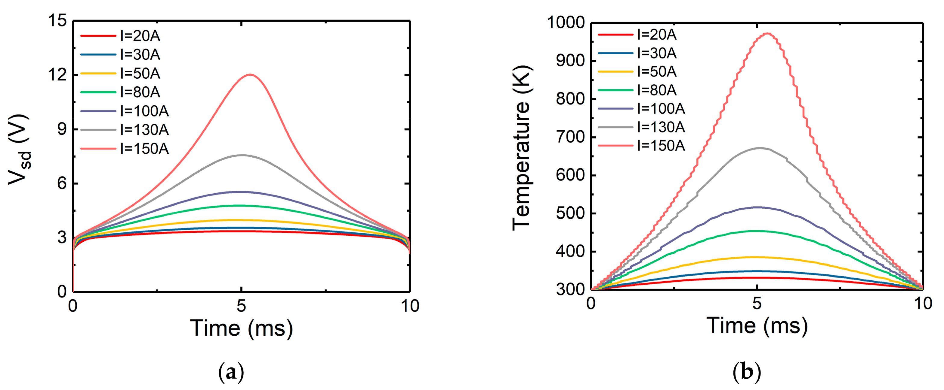
Plotted in Figure 15a is the variation of Vsd with time inside the device. Initially, there is a voltage jump. This phenomenon matches the experimental results, as shown in Figure 4. In the channel off mode, only the body diode is conducting, and the body diode will not conduct until the threshold voltage is reached. Therefore, there is a voltage jump in the beginning.
Figure 15b shows the change of maximum temperature inside the device with time under different surge current conditions. It can be seen that the trend of the maximum temperature is roughly consistent with that of the voltage. When the current peak value increases, the maximum temperature rises gradually. It can also be found that the temperature rises faster with the increase of current peak value.
The Channel Conduction Mode
The simulated curve of Vsd with time in the channel conduction mode is shown in Figure 16a. In Figure 16a, there is an obvious turning point on the voltage curve. In the channel conduction mode, at low current peak value the current flows through the channel. However, as the surge current increases, Vsd exceeds the body diode threshold voltage and the body diode conducts current as well. In the experiments, this turning point is not so obvious due to the influence of the parasitic capacitance and inductance. Shown in Figure 16b is the variation of internal maximum temperature with time in the channel conduction mode. The curve is similar to the case when the channel is not conducting.
The current densities in the body diode region and the channel when the channel was conducting have been simulated to find out the reasons why channel conduction had little effect on the device surge tolerance. The simulation results are shown in Figure 17. At low current peak value, the current flows through the channel only. When the on-set voltage of body diode is reached, a portion of the current was transferred to the body diode region. It can be noticed that the slope of the current density flowing through the channel is decreased. Finally, the current density in the body diode becomes greater than the current density in the channel. Shown in Figure 17b are the current flowlines inside the device at t = 5 ms. The number of current flowlines is proportional to the current density. It can be seen that the number of the current flowlines in the body diode region is much more than that in the channel. From Figure 17, it is found that when the current is large enough, the current mainly passes through the body diode region.
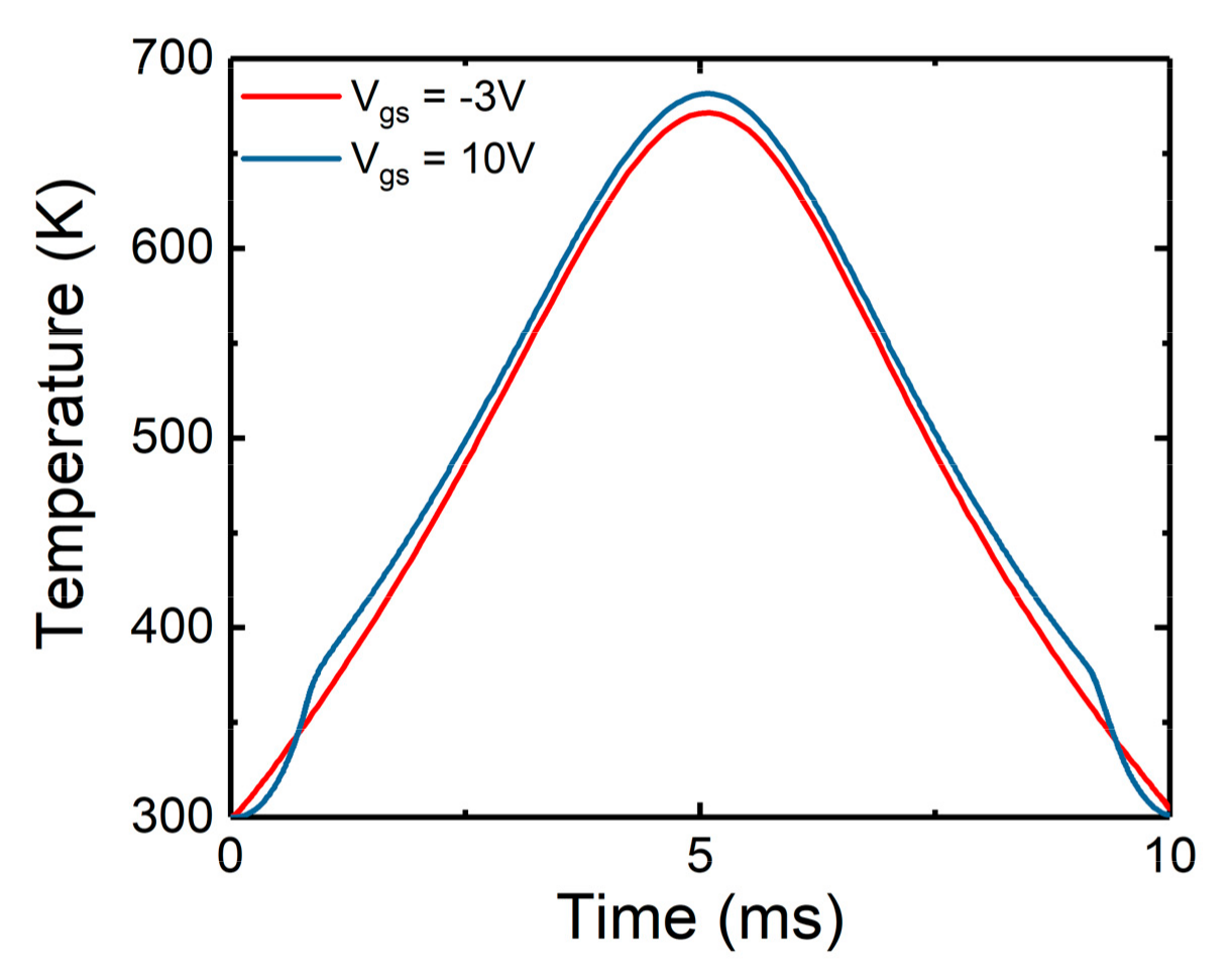
It is found in the previous sections that the surge failure in this study is mainly caused by the high junction temperature. The maximum junction temperatures versus the time under channel conduction and non-conduction modes are compared in Figure 18. It can be seen that the maximum temperatures on conduction mode are slightly higher than that on the non-conduction mode. Therefore, it can be concluded that no matter the channel is conducting or not, the maximum junction temperatures inside the device are similar. As a result, the surge tolerance is approximately equal. This is mainly due to the fact that, when the current is big enough, the body diode current dominates against the MOS channel current. It also can be seen that, with the increase of the current, the maximum temperature inside the device could exceed the melting point of Al (933 K) and lead to the melting of Al.
5. Conclusions
In summary, the reverse conduction surge reliability of several 1200 V SiC MOSFETs has been tested in the channel conduction and non-conduction modes in this paper. Device failures under these circumstances have been investigated in detail. Two types of failure characterized by different behavior after the failure have been found. It is demonstrated that during the surge event the excessive heat causes the melting of Aluminum and its subsequent reaction with and penetration into the SiC device and dielectric layers. Open-cover anatomy and 2-D numerical simulation confirms such mechanisms.
By increasing the surge current gradually until failure, it is found that the maximum surge currents that the devices can withstand are similar for both channel conduction and non-conduction modes.
The performance change of the device after failure is mainly reflected in two aspects: The first is the short circuit between the gate and the source, the other is the performance change of the body diode. Although the threshold voltages of the body diodes in all devices have been lowered after the failure, the reverse blocking characteristics of the body diodes are different. The reverse blocking capability of Cree’s devices represented by C2M0160120D remain essentially unchanged, while other devices represented by SCT10N120 lost their reverse blocking capability after the surge failure. Then, the static characteristics of the device have been tested after each surge current was applied to help understanding the process of the failure. It is found that almost no damage occurred to the gate oxide and the body diode region until the maximum surge current was applied.
The open-cover anatomy of the two devices has been carried out. Both devices have burn marks, but the degree of damage is lighter for the Cree device. Increasing the number of bonding wires can spread the current more evenly across the chip and relieve damage caused by high temperature. By observing the cross section of the damaged cell, it is found that when the surge failure occurs, the source metal melts and penetrates into the interlayer dielectric and the P-well region, leading to the failure of the device.
Silvaco finite element numerical simulation has been employed to study the variation of the internal temperature and current density during the surge tests. In the simulation, it is found that when the surge current reaches a large value, the current mainly flows through the body diode. Therefore, whether the channel conducts or not has limited effect on the surge capability. This conclusion is consistent with the experimental results.
Author Contributions
Conceptualization, H.L. and K.S.; Data curation, H.L.; Formal analysis, H.L. and J.W.; Funding acquisition, J.W.; Methodology, J.W. and N.R.; Project administration, J.W.; Supervision, J.W. and K.S.; Validation, H.L. and H.X.; Writing—original draft, H.L.; Writing—review & editing, J.W., N.R. and K.S.
Funding
This research was funded by grants from the National Natural Science Foundation of China (grant number 51877198).
Conflicts of Interest
The authors declare no conflict of interest.
References
- Chow, T.P.; Tyagi, R. Wide bandgap compound semiconductors for superior high-voltage power devices. In Proceedings of the 5th International Symposium on Power Semiconductor Devices and ICs, Monterey, CA, USA, 18–20 May 1993; pp. 84–88. [Google Scholar] [CrossRef]
- Chow, T.P.; Tyagi, R. Wide bandgap compound semiconductors for superior high-voltage unipolar power devices. IEEE Trans. Electron. Devices 1994, 8, 1481–1483. [Google Scholar] [CrossRef]
- Chow, T.P.; Si, C.; Ga, N. High-voltage power switching devices. Mater. Sci. Forum 2000, 338, 1155–1160. [Google Scholar] [CrossRef]
- Casady, J.B.; Johnson, R.W. Status of silicon carbide (SiC) as a wide-bandgap semiconductor for high-temperature applications: A review. Solid-State Electron. 1996, 39, 1409–1422. [Google Scholar] [CrossRef]
- Saremi, M. modeling and Simulation of the Programmable Metallization Cells (pmcs) and Diamond-Based Power Devices. Ph.D. Thesis, Arizona State University, Tempe Campus, AZ, USA, 2017. [Google Scholar]
- Aminbeidokhti, A.; Dimitrijev, S.; Hanumanthappa, A.K.; Moghadam, H.A.; Haasmann, D.; Han, J.; Xu, X. Gate-voltage independence of electron mobility in power AlGaN/GaN HEMTs. IEEE Trans. Electron Devices 2016, 63, 1013–1019. [Google Scholar] [CrossRef]
- Aminbeidokhti, A.; Dimitrijev, S.; Hanumanthappa, A.K.; Moghadam, H.A.; Haasmann, D.; Han, J.; Xu, X. The power law of phonon-limited electron mobility in the 2-D electron gas of AlGaN/GaN heterostructure. IEEE Trans. Electron. Devices 2016, 63, 2214–2218. [Google Scholar] [CrossRef]
- Kimoto, T.; Kosugi, H.; Suda, J.; Kanzaki, Y.; Matsunami, H. Design and fabrication of resurf MOSFETs on 4H-SiC and 6H-SiC. IEEE Trans. Electron. Devices 2005, 52, 112–117. [Google Scholar] [CrossRef]
- Wondrak, W.; Held, R.; Niemann, E.; Schmid, U. SiC devices for advanced power and high-temperature applications. IEEE Trans. Ind. Electron. 2001, 48, 307–308. [Google Scholar] [CrossRef]
- Palanisamy, S.; Fichtner, S.; Lutz, J.; Basler, T.; Rupp, R. Various structures of 1200V SiC MPS diode models and their simulated surge current behavior in comparison to measurement. In Proceedings of the 2016 28th International Symposium on Power Semiconductor Devices and ICs (ISPSD), Prague, Czech Republic, 12–16 June 2016; pp. 235–238. [Google Scholar] [CrossRef]
- Kowalsky, J.; Simon, T.; Geske, M.; Basler, T.; Lutz, J. Surge Current Behaviour of Different IGBT Designs. In Proceedings of the PCIM Europe 2015, International Exhibition and Conference for Power Electronics, Intelligent Motion, Renewable Energy and Energy Management, Nuremberg, Germany, 19–21 May 2015; pp. 1–10. [Google Scholar]
- Basler, T.; Lutz, J.; Jakob, R.; Brückner, T. Surge current capability of IGBTs. In Proceedings of the International Multi-Conference on Systems, Sygnals & Devices, Chemnitz, Germany, 20–23 March 2012; pp. 1–6. [Google Scholar] [CrossRef]
- Basler, T.; Lutz, J.; Jakob, R. IGBTs conducting diode-like surge currents. In Proceedings of the 2014 IEEE 26th International Symposium on Power Semiconductor Devices & IC’s (ISPSD), Waikoloa, HI, USA, 15–19 June 2014; pp. 103–106. [Google Scholar] [CrossRef]
- Radhakrishnan, R.; Cueva, N.; Witt, T.; Woodin, R.L. Analysis of forward surge performance of sic schottky diodes. Mater. Sci. Forum 2018, 924, 621–624. [Google Scholar] [CrossRef]
- Hilsenbeck, J.; Treu, M.; Rupp, R.; Rüschenschmidt, K.; Kern, R.; Holz, M. Investigations on surge current capability of SiC schottky diodes by implementation of new pad metallizations. Mater. Sci. Forum 2010, 645, 673–676. [Google Scholar] [CrossRef]
- Banu, V.; Godignon, P.; Jordá, X.; Alexandru, M.; Millan, J. SiC schottky diode surge current analysis and application design using behavioral SPICE models. In Proceedings of the CAS 2012 (International Semiconductor Conference), Sinaia, Romania, 15–17 October 2012; pp. 359–362. [Google Scholar] [CrossRef]
- León, J.; Perpiñà, X.; Banu, V.; Montserrat, J.; Berthou, M.; Vellvehí, M.; Jordà, X. Temperature effects on the ruggedness of SiC schottky diodes under surge current. Microelectron. Reliab. 2014, 54, 2207–2212. [Google Scholar] [CrossRef]
- Hofstetter, P.; Bakran, M.M. Predicting Failure of SiC MOSFETs under short circuit and surge current conditions with a single thermal model. In Proceedings of the IEEE 20th European Conference on Power Electronics and Applications (EPE’18 ECCE Europe), Riga, Latvia, 17–21 September 2018; pp. 1–9. [Google Scholar]
- Sadik, D.P.; Heinig, S.; Jacobs, K.; Johannesson, D.; Lim, J.K.; Nawaz, M.; Dijkhuizen, F.; Bakowski, M.; Norrga, S.; Nee, H.P. Investigation of the surge current capability of the body diode of SiC MOSFETs for HVDC applications. In Proceedings of the European Conference on Power Electronics & Applications, Karlsruhe, Germany, 5–9 September 2016; pp. 1–10. [Google Scholar] [CrossRef]
- Rodrigues, R.; Zhang, Y.; Jiang, T.; Aeloiza, E.; Cairoli, P. Surge current capability of SiC MOSFETs in AC distribution systems. In Proceedings of the IEEE 6th Workshop on Wide Bandgap Power Devices and Applications (WiPDA), Atlanta, GA, USA, 31 October–2 November 2018; pp. 331–337. [Google Scholar]
- Carastro, F.; Mari, J.; Zoels, T.; Rowden, B.; Losee, P.; Stevanovic, L. Investigation on diode surge forward current ruggedness of Si and SiC power modules. In Proceedings of the European Conference on Power Electronics & Applications, Karlsruhe, Germany, 5–9 September 2016; pp. 1–10. [Google Scholar] [CrossRef]
- Shan, Y.; Yunfei, G.; Shuairong, D.; Xiong, X.; Gang, D. Comparative Investigation of Surge Current Capabilities of Si IGBT and SiC MOSFET for Pulsed Power Application. IEEE Trans. Plasma Sci. 2018, 1–6. [Google Scholar] [CrossRef]
- Hofstetter, P.; Bakran, M.M. Comparison of the surge current ruggedness between the body diode of sic mosfets and si diodes for igbt. In Proceedings of the 10th International Conference on Integrated Power Electronics Systems (CIPS 2018), Stuttgart, Germany, 20–22 March 2018; pp. 1–7. [Google Scholar]
- Jiang, X.; Zhai, D.; Chen, J.; Yuan, F.; Li, Z.; He, Z.; Wang, J. Comparison study of surge current capability of body diode of SiC MOSFET and SiC schottky diode. In Proceedings of the IEEE Energy Conversion Congress and Exposition (ECCE), Portland, OR, USA, 23–27 September 2018; pp. 845–849. [Google Scholar]
- Yamamoto, S.; Nakao, Y.; Tomita, N.; Nakata, S.; Yamakawa, S. Development of 3.3 kV SiC-MOSFET:Suppression of forward voltage degradation of the body diode. Mater. Sci. Forum 2014, 4, 778–780. [Google Scholar] [CrossRef]
- Imaizumi, M.; Miura, N. Characteristics of 600, 1200, and 3300 V planar SiC-MOSFETs for energy conversion applications. IEEE Trans. Electron. Devices 2014, 62, 390–395. [Google Scholar] [CrossRef]
- Hull, B.; Allen, S.; Zhang, S.; Gajewski, D.; Pala, V.; Richmond, J.; Ryu, S.; O’Loughlin, M.; Van, B.E.; Cheng, L.; et al. Reliability and stability of SiC power mosfets and nextgeneration SiC MOSFETs. In Proceedings of the IEEE Workshop on Wide Bandgap Power Devices and Applications, Knoxville, TN, USA, 13–15 October 2014; pp. 139–142. [Google Scholar] [CrossRef]
- Sadik, D.; Lim, J.; Ranstad, P.; Nee, H. Investigation of long-term parameter variations of SiC power MOSFETs. In Proceedings of the 17th European Conference on Power Electronics and Applications, Geneva, Switzerland, 8–10 September 2015; pp. 1–10. [Google Scholar] [CrossRef]
- Callanan, R.; Rice, J.; Palmour, J. Third quadrant behavior of SiC MOSFETs. In Proceedings of the 28th Annual IEEE Applied Power Electronics Conference and Exposition, Long Beach, CA, USA, 17–21 March 2013; pp. 1250–1253. [Google Scholar] [CrossRef]
- Hunger, T.; Schilling, O.; Wolter, F. Numerical and experimental study on surge current limitations of wire-bonded power diodes. In Proceedings of the PCIM Europe 2007, Nuremburg, Germany, 22–24 May 2007. [Google Scholar]
- Schroder, D.K. Semiconductor Material and Device Characterization; John Wiley & Sons, Inc.: Hoboken, NJ, USA, 2006; pp. 370–372. [Google Scholar] [CrossRef]
- Heinze, B.; Lutz, J.; Rupp, R.; Holz, M. Surge current ruggedness of silicon carbide Schottky and merged-PiN-Schottky Diodes. In Proceedings of the 20th International Symposium on Power Semiconductor Devices, Orlando, FL, USA, 18–22 May 2008; pp. 245–248. [Google Scholar] [CrossRef]
- Silber, D.; Robertson, M.J. Thermal effects on the forward characteristic of silicon PiN diodes at high pulse currents. Solid State Electron. 1973, 16, 1337–1346. [Google Scholar] [CrossRef]
- Fichtner, S.; Lutz, J.; Basler, T.; Rupp, R.; Gerlach, R. Electro-thermal simulations and experimental results on the surge current capability of 1200 V SiC MPS diodes. In Proceedings of the International Conference on Integrated Power Electronics Systems, Nuremberg, Germany, 25–27 February 2014; pp. 1–5, ISBN 978-3-8007-3578-5. [Google Scholar]
- Berger, W.M.; Keen, R.S.; Schnable, G.L. Reliability phenomena in aluminum metalizations on silicon dioxide. In Proceedings of the 4th Symposium on the Physics of Failure in Electronics, Chicago, IL, USA, 16–18 November 1965; pp. 1–31. [Google Scholar] [CrossRef]
- Black, J.R. Electromigration of Al-Si alloy films. In Proceedings of the 15th International Reliability Physics Symposium, San Diego, CA, USA, 18–20 April 1978; pp. 257–261. [Google Scholar] [CrossRef]
- Tanimoto, S.; Ohashi, H. Reliability issues of SiC power MOSFETs toward high junction temperature operation. Phys. Status Solidi A 2009, 206, 2417–2430. [Google Scholar] [CrossRef]
- Roccaforte, F.; Via, F.L.; Raineri, V. Ohmic Contacts to SIC. Int. J. High Speed Electron. Syst. 2005, 15, 781–820. [Google Scholar] [CrossRef]
- Kakanakov, R.; Kassamakova-Kolaklieva, L.; Hristeva, N.; Lepoeva, G.; Zekentes, K. Thermally stable low resistivity ohmic contacts for high power and high temperature SiC device applications. In Proceedings of the 23rd International Conference on Microelectronics. Proceedings (Cat. No. 02TH8595), Nis, Yugoslavia, 12–15 May 2002. [Google Scholar] [CrossRef]
- HKelek, E.; Robinson, G.Y. Aluminum/nickel silicide contacts on silicon. Thin Solid Films 1978, 53, 135–140. [Google Scholar] [CrossRef]
- Bartur, M.; Nicolet, M.A. Thermal oxidation of nickel disilicide. Appl. Phys. Lett. 1982, 40, 175–177. [Google Scholar] [CrossRef] [Green Version]
Figure 1.
Cell structure of SiC metal-oxide-semiconductor field-effect transistor (MOSFET).

Figure 2.
(a) Transfer characteristic with Vds = 10 V and (b) reverse I-V curves of C2M0160120D from Cree.
Figure 2.
(a) Transfer characteristic with Vds = 10 V and (b) reverse I-V curves of C2M0160120D from Cree.

Figure 3.
(a) Simplified schematic of the surge current test circuit, (b) the waveform of the surge current.
Figure 3.
(a) Simplified schematic of the surge current test circuit, (b) the waveform of the surge current.

Figure 4.
The variation of voltage Vsd of (a) SCT10N20, (b) C2M0080120D, (c) C2M0160120D, (d) LSIC1MO120E0160, (e) SCT3160KLGC11 SiC MOSFETs when varying surge current amplitude with Vgs = −3 V.
Figure 4.
The variation of voltage Vsd of (a) SCT10N20, (b) C2M0080120D, (c) C2M0160120D, (d) LSIC1MO120E0160, (e) SCT3160KLGC11 SiC MOSFETs when varying surge current amplitude with Vgs = −3 V.

Figure 5.
The variation of voltage Vsd of (a) SCT10N20, (b) C2M0080120D, (c) C2M0160120D, (d) LSIC1MO120E0160, (e) SCT3160KLGC11 SiC MOSFETs when varying surge current amplitude with Vgs = 10 V.
Figure 5.
The variation of voltage Vsd of (a) SCT10N20, (b) C2M0080120D, (c) C2M0160120D, (d) LSIC1MO120E0160, (e) SCT3160KLGC11 SiC MOSFETs when varying surge current amplitude with Vgs = 10 V.

Figure 6.
The characteristics of SiC MOSFET’s body diode (SCT10N120) before and after the failure (a) forward conduction characteristics, (b) reverse blocking characteristics.
Figure 6.
The characteristics of SiC MOSFET’s body diode (SCT10N120) before and after the failure (a) forward conduction characteristics, (b) reverse blocking characteristics.

Figure 7.
The characteristics of SiC MOSFET’s body diode (C2M1060120D) before and after the failure (a) forward conduction characteristics, (b) reverse blocking characteristics.
Figure 7.
The characteristics of SiC MOSFET’s body diode (C2M1060120D) before and after the failure (a) forward conduction characteristics, (b) reverse blocking characteristics.

Figure 8.
(a) Transfer characteristics, (b) sub-threshold swing characteristics, (c) forward conduction characteristics of the body diode of SCT10N120 after each surge test.
Figure 8.
(a) Transfer characteristics, (b) sub-threshold swing characteristics, (c) forward conduction characteristics of the body diode of SCT10N120 after each surge test.

Figure 9.
(a) Transfer characteristic, (b) sub-threshold swing characteristics, (c) forward conduction characteristics of the body diode of C2M0160120D after each surge test.
Figure 9.
(a) Transfer characteristic, (b) sub-threshold swing characteristics, (c) forward conduction characteristics of the body diode of C2M0160120D after each surge test.

Figure 10.
The anatomy results of STM device SCT10N120 (a) decapping, (b) removing layers to the substrate layer.
Figure 10.
The anatomy results of STM device SCT10N120 (a) decapping, (b) removing layers to the substrate layer.
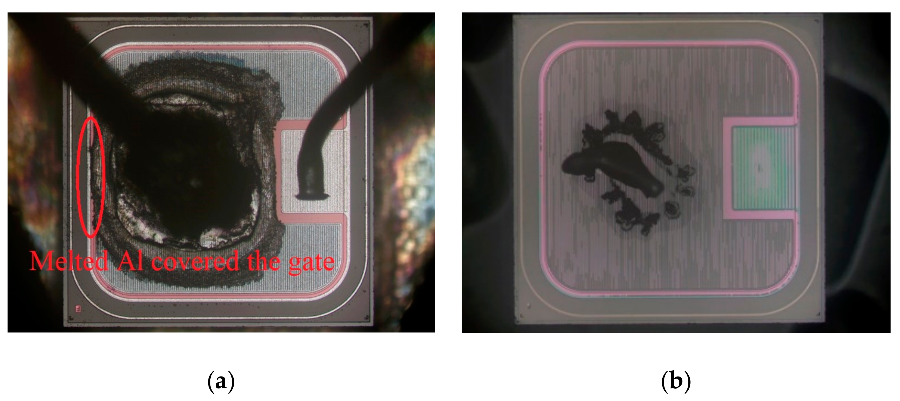
Figure 11.
The anatomy results of Cree device C2M0160120D (a) decapping, (b) removing layers to the substrate layer.
Figure 11.
The anatomy results of Cree device C2M0160120D (a) decapping, (b) removing layers to the substrate layer.

Figure 12.
SEM images of SCT10N120 (a) before, (b) after the device failure.

Figure 13.
SEM images of C2M0160120D (a) before, (b) after the device failure.

Figure 14.
Comparison of (a) transfer characteristics, (b) body diode characteristics, between simulation and test result.
Figure 14.
Comparison of (a) transfer characteristics, (b) body diode characteristics, between simulation and test result.

Figure 15.
When the channel is non-conducting, the simulated (a) source-drain voltage, (b) maximum temperature, with time.
Figure 15.
When the channel is non-conducting, the simulated (a) source-drain voltage, (b) maximum temperature, with time.

Figure 16.
When the channel is conducting, the simulated variation of (a) source-drain voltage, (b) maximum temperature versus time.
Figure 16.
When the channel is conducting, the simulated variation of (a) source-drain voltage, (b) maximum temperature versus time.

Figure 17.
(a) Current density of body diode region and channel versus time. (b) Current flowlines in device when time = 5 ms.
Figure 17.
(a) Current density of body diode region and channel versus time. (b) Current flowlines in device when time = 5 ms.

Figure 18.
Comparison of the maximum temperature under channel conduction and non-conduction modes when Is = 130 A.
Figure 18.
Comparison of the maximum temperature under channel conduction and non-conduction modes when Is = 130 A.

Table 1.
Structure parameters of the metal-oxide-semiconductor field-effect transistor (MOSFET) shown in Figure 1.
Table 1.
Structure parameters of the metal-oxide-semiconductor field-effect transistor (MOSFET) shown in Figure 1.
| Region | Numerical Value | Unit |
|---|---|---|
| Doping concentration in P−well region | Surface , internal peak 1 | cm−3 |
| Depth of P−well region | 0.5 | |
| Doping concentration in N− drift region | cm−3 | |
| Depth of N- drift region | 10 | |
| Doping concentration in N++ substrate region | cm−3 | |
| Depth of N++ substrate region | 170 | |
| Doping concentration in N+ region | cm−3 | |
| Depth of N+ region | 0.2 | |
| Doping concentration in P+ region | cm−3 | |
| Length of channel | 0.96 | |
| Thickness of gate oxide layer | 0.05 | |
| Length of junction field-effect transistor (JFET) region | 2.4 |
Table 2.
Device parameters from the datasheets.
| Vds (V) | Rds(on) (mΩ) | Ids (A)/ Body Diode IF (A) | Vgs (V) | Vth (V) | |
|---|---|---|---|---|---|
| SCT10N120 | 1200 | 500 | 12/12 | −10/25 | 5.5 |
| C2M0080120D | 1200 | 80 | 36/36 | −5/20 | 2.8 |
| C2M0160120D | 1200 | 160 | 19/19 | −5/20 | 3 |
| LSIC1MO120E0160 | 1200 | 160 | 22/22 | −5/20 | 3.6 |
| SCT3160KLGC11 | 1200 | 160 | 17/17 | −4/22 | 5 |
Table 3.
Maximum surge current that a device can withstand.
| Ids (A)/ Body Diode IF (A) | Rds(on) (mΩ) | Maximum Surge Current (A) | Maximum Surge Current/Rated Current | |
|---|---|---|---|---|
| SCT10N120 | 12/12 | 500 | 61 | 5 |
| C2M0080120D | 36/36 | 80 | 155 | 4.3 |
| C2M0160120D | 19/19 | 160 | 105 | 5.5 |
| LSIC1MO120E0160 | 22/22 | 160 | 95 | 4.3 |
| SCT3160KLGC11 | 17/17 | 160 | 42 | 2.5 |
Table 4.
Measured resistances between electrodes before and after surge tests.
| Device | Rgs (Ω) | Rds (Ω) |
|---|---|---|
| Before the tests | >100 M | >100 M |
| SCT10N120, after tests | 0.4 | 14 k |
| C2M0160120D, after tests | 0.08 | >100 M |
Table 5.
Physical models used in simulation.
| Model | Model Used in Simulation | Notes |
|---|---|---|
| Carrier Statistics Models | Fermi-Dirac | Reduced carrier concentrations in heavily doped regions (statistical approach). |
| Bandgap Narrowing(BGN) | Important in heavily doped regions. Critical for bipolar gain. Use Klaassen Model. | |
| Mobility Models | Lombardi (CVT) Model | Complete model including N, T, E//, and E┴ effects. * |
| Recombination Models | Shockley-Read-Hall(SRH) | Uses fixed minority carrier lifetimes. |
| Auger | Direct transition of three carriers. Important at high current densities. | |
| Impact Ionization Model | Selberherr’s Model (Impact selb) | Recommended for most cases. Includes temperature dependent parameters. |
* T is lattice temperature, N is the dopant concentration, E// is parallel electric field, and E┴ is perpendicular electric field.
© 2019 by the authors. Licensee MDPI, Basel, Switzerland. This article is an open access article distributed under the terms and conditions of the Creative Commons Attribution (CC BY) license (http://creativecommons.org/licenses/by/4.0/).
Share and Cite
MDPI and ACS Style
Li, H.; Wang, J.; Ren, N.; Xu, H.; Sheng, K. Investigation of 1200 V SiC MOSFETs’ Surge Reliability. Micromachines 2019, 10, 485. https://doi.org/10.3390/mi10070485
AMA Style
Li H, Wang J, Ren N, Xu H, Sheng K. Investigation of 1200 V SiC MOSFETs’ Surge Reliability. Micromachines. 2019; 10(7):485. https://doi.org/10.3390/mi10070485
Chicago/Turabian StyleLi, Huan, Jue Wang, Na Ren, Hongyi Xu, and Kuang Sheng. 2019. "Investigation of 1200 V SiC MOSFETs’ Surge Reliability" Micromachines 10, no. 7: 485. https://doi.org/10.3390/mi10070485
Note that from the first issue of 2016, this journal uses article numbers instead of page numbers. See further details here.